19-1533; Rev 2; 12/02
KIT
ATION
EVALU
E
L
B
A
AVAIL
420ksps, +5V, 6-/2-Channel, 12-Bit ADCs
with +2.5V Reference and Parallel Interface
Power consumption is only 10mW at the maximum sampling rate of 420ksps. Two software-selectable powerdown modes enable the MAX1294/MAX1296 to be shut
down between conversions; accessing the parallel
interface returns them to normal operation. Powering
down between conversions can reduce supply below
10µA at lower sampling rates.
Both devices offer software-configurable analog inputs for
unipolar/bipolar and single-ended/pseudo-differential
operation. In single-ended mode, the MAX1294 has six
input channels and the MAX1296 has two (three input
channels and one input channel, respectively, when in
pseudo-differential mode).
Excellent dynamic performance and low power, combined with ease of use and small package size, make
these converters ideal for battery-powered and dataacquisition applications or for other circuits with demanding power-consumption and space requirements.
The MAX1294/MAX1296 tri-states INT when CS goes
high. Refer to MAX1266/MAX1268 if tri-stating INT is not
desired.
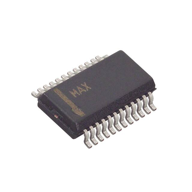
The MAX1294 is offered in a 28-pin QSOP package, while
the MAX1296 is available in a 24-pin QSOP. For pin-compatible +3V, 12-bit versions, see the MAX1295/MAX1297.
Applications
Features
♦ 12-Bit Resolution, ±0.5 LSB Linearity
♦ Single +5V Operation
♦ Internal +2.5V Reference
♦ Software-Configurable Analog Input Multiplexer
6-Channel Single-Ended/
3-Channel Pseudo-Differential (MAX1294)
2-Channel Single-Ended/
1-Channel Pseudo-Differential (MAX1296)
♦ Software-Configurable Unipolar/Bipolar
Analog Inputs
♦ Low Current
2.8mA (420ksps)
1.0mA (100ksps)
400µA (10ksps)
2µA (Shutdown)
♦ Internal 6MHz Full-Power Bandwidth Track/Hold
♦ Parallel 12-Bit Interface
♦ Small Footprint
28-Pin QSOP (MAX1294)
24-Pin QSOP (MAX1296)
Pin Configurations
TOP VIEW
D9 1
24 D10
D8 2
23 D11
Industrial Control Systems
Data Logging
D7 3
22 VDD
Energy Management
Patient Monitoring
D6 4
21 REF
Touchscreens
D5 5
Data-Acquisition Systems
Ordering Information
PART
TEMP RANGE
MAX1294ACEI
0°C to +70°C
PIN-PACKAGE
28 QSOP
INL
(LSB)
±0.5
D4 6
20 REFADJ
MAX1296
19 GND
D3 7
18 COM
D2 8
17 CH0
D1 9
16 CH1
15 CS
MAX1294BCEI
0°C to +70°C
28 QSOP
±1
D0 10
MAX1294AEEI
-40°C to +85°C
28 QSOP
±0.5
INT 11
14 CLK
MAX1294BEEI
-40°C to +85°C
28 QSOP
±1
RD 12
13 WR
MAX1296ACEG
0°C to +70°C
24 QSOP
±0.5
MAX1296BCEG
0°C to +70°C
24 QSOP
±1
MAX1296AEEG -40°C to +85°C
24 QSOP
±0.5
MAX1296BEEG -40°C to +85°C
24 QSOP
±1
QSOP
Pin Configurations continued at end of data sheet.
Typical Operating Circuits appear at end of data sheet.
________________________________________________________________ Maxim Integrated Products
For pricing, delivery, and ordering information, please contact Maxim/Dallas Direct! at
1-888-629-4642, or visit Maxim’s website at www.maxim-ic.com.
1
MAX1294/MAX1296
General Description
The MAX1294/MAX1296 low-power, 12-bit analog-todigital converters (ADCs) feature a successive-approximation ADC, automatic power-down, fast wake-up
(2µs), an on-chip clock, +2.5V internal reference, and a
high-speed 12-bit parallel interface. They operate with
a single +5V analog supply.
�MAX1294/MAX1296
420ksps, +5V, 6-/2-Channel, 12-Bit ADCs
with +2.5V Reference and Parallel Interface
ABSOLUTE MAXIMUM RATINGS
VDD to GND ..............................................................-0.3V to +6V
CH0–CH5, COM to GND ............................-0.3V to (VDD + 0.3V)
REF, REFADJ to GND.................................-0.3V to (VDD + 0.3V)
Digital Inputs to GND ...............................................-0.3V to +6V
Digital Outputs (D0–D11, INT) to GND.......-0.3V to (VDD + 0.3V)
Continuous Power Dissipation (TA = +70°C)
24-Pin QSOP (derate 9.5mW/°C above +70°C)..........762mW
28-Pin QSOP (derate 8.00mW/°C above +70°C)........667mW
Operating Temperature Ranges
MAX1294_C_ _/MAX1296_C_ _ .........................0°C to +70°C
MAX1294_E_ _/MAX1296_E_ _ ......................-40°C to +85°C
Storage Temperature Range .............................-65°C to +150°C
Lead Temperature (soldering, 10s) .................................+300°C
Stresses beyond those listed under “Absolute Maximum Ratings” may cause permanent damage to the device. These are stress ratings only, and functional
operation of the device at these or any other conditions beyond those indicated in the operational sections of the specifications is not implied. Exposure to
absolute maximum rating conditions for extended periods may affect device reliability.
ELECTRICAL CHARACTERISTICS
(VDD = +5V ±10%, COM = GND, REFADJ = VDD, VREF = +2.5V, 4.7µF capacitor at REF pin, fCLK = 7.6MHz (50% duty cycle),
TA = TMIN to TMAX, unless otherwise noted. Typical values are at TA = +25°C.)
PARAMETER
SYMBOL
CONDITIONS
MIN
TYP
MAX
UNITS
DC ACCURACY (Note 1)
Resolution
RES
Relative Accuracy (Note 2)
INL
Differential Nonlinearity
DNL
12
Bits
MAX129_A
±0.5
MAX129_B
±1
No missing codes over temperature
±1
LSB
±4
LSB
Offset Error
±4
Gain Error (Note 3)
LSB
LSB
Gain Temperature Coefficient
±2.0
ppm/°C
Channel-to-Channel Offset
Matching
±0.2
LSB
DYNAMIC SPECIFICATIONS (fIN(sine wave) = 50kHz, VIN = 2.5VP-P, 420ksps, external fCLK = 7.6MHz, bipolar input mode)
Signal-to-Noise Plus Distortion
SINAD
Total Harmonic Distortion
(including 5th-order harmonic)
THD
Spurious-Free Dynamic Range
SFDR
67
70
dB
-80
-80
dB
dB
fIN1 = 49kHz, fIN2 = 52kHz
76
Channel-to-Channel Crosstalk
fIN = 175kHz (Note 4)
-78
dB
Full-Linear Bandwidth
SINAD > 68dB
350
kHz
Full-Power Bandwidth
-3dB rolloff
6
MHz
Intermodulation Distortion
IMD
dB
CONVERSION RATE
Conversion Time (Note 5)
T/H Acquisition Time
tCONV
2
External acquisition/internal clock mode
2.5
3.0
3.5
Internal acquisition/internal clock mode
3.2
3.6
4
400
External acquisition or external clock mode
Aperture Jitter
Duty Cycle
2.1
tACQ
Aperture Delay
External Clock Frequency
External clock mode
fCLK
25
External acquisition or external clock mode
很抱歉,暂时无法提供与“MAX1296BCEG”相匹配的价格&库存,您可以联系我们找货
免费人工找货