MAX14001/MAX14002
Evaluation System
General Description
The MAX14001/14002 evaluation system (EV system)
provides the hardware and software necessary to evaluate
the MAX14001 and MAX14002 isolated, single-channel,
analog-to-digital converters (ADCs) with programmable
voltage comparators and inrush current control optimized
for configurable binary input applications. The MAX14001/
MAX14002 EV kit has Pmod™ compatible connectors
for SPI communication. The EV system includes the
USB2PMB2 adapter board that receives commands
from a PC through the USB cable to create an SPI
interface for communication between the software and the
MAX14001/MAX14002 on the EV kit.
The EV system includes a graphical user interface (GUI)
that provides communication between the target device
and the PC. The MAX14001/MAX14002 EV kit has two
MAX14001/MAX14002 devices (U1 and U2) that can
operate in multiple modes, as shown in Figure 1:
Evaluates: MAX14001, MAX14002
Benefits and Features
●● Easy Evaluation of the MAX14001/MAX14002
●● EV Kit is USB Powered
●● Daisy-Chainable SPI Interface
●● Internal Voltage Reference or External Voltage
Reference
●● Half-Wave Input Rectification Filter or Full-Wave
Input Rectification Filter
●● Windows XP®, Windows® 7, Windows 8.1, and
Windows 10 Compatible Software
●● Fully Assembled and Tested
●● Proven PCB Layout
●● RoHS Compliant
Ordering Information appears at end of data sheet.
1) Single Channel mode: The USB2PMB2 adapter
connects to connector PMOD1 or PMOD2 on the
EV kit, depending on which channel is preferred,
allowing differently configured analog inputs with
signal conditioning circuitry.
2) Daisy-Chain mode: The USB2PMB2 adapter
connects to connector PMOD1, and DOUT from U1
connects to DIN of U2. Both U1 and U2 are controlled
from a single SPI interface.
3) Dual Channel mode: The USB2PMB2 adapter
connects to connector PMOD1 and uses two chipselect signals (CS1 and CS2) to control each chip
through a single connector/GUI interface.
EV System Contents
●● MAX14001EVKIT#, including the MAX14001AAP+ or
MAX14002EVKIT#, including the MAX14002AAP+
●● USB2PMB2# Adapter Board
●● Micro-USB Cable
Windows and Windows XP are registered trademarks and
registered service marks of Microsoft Corporation.
Pmod is a trademark of Digilent, Inc
19-8690; Rev 0; 11/16
�MAX14001/MAX14002
Evaluation System
Evaluates: MAX14001, MAX14002
MAX14001/MAX14002 EV Kit Photo
USB2PMB2 Adapter Board Photo
www.maximintegrated.com
Maxim Integrated │ 2
�MAX14001/MAX14002
Evaluation System
Evaluates: MAX14001, MAX14002
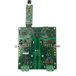
MAX14001/MAX14002 EV System Photo
Note: Board standoffs and screws are not included in the EV system.
www.maximintegrated.com
Maxim Integrated │ 3
�Evaluates: MAX14001, MAX14002
MAX14001/MAX14002
Evaluation System
System Block Diagram
FIELD-SIDE
LOGIC-SIDE
SERIES VREF
U3
AGND 1
300VDC NOMINAL
T1
FULL-WAVE
RECTIFIER
RESISTORDIVIDER
J10
J3
EXT AIN
VDDF
VDD
SHUNT
VREF
AGND 1
COUT
COUT 1
PMOD 1
U1
120KΩ
GNDF 1
AGND 1
T2
RESISTORDIVIDER
SERIES VREF
U7
AGND 2
J29
J28
U6
SHUNT
VREF
AGND 2
DEPLETION MODE
FET Q 2
MISO 1
VDDF
120KΩ
GNDF 2
OPERATING
MODES
3.3V_P2
VDD
VDDL
JUMPER
SETTING
3.3V_P2
REFIN
VDD
AGND
U2
IFET
GNDF 2
GNDL
GNDL
JUMPER
SETTING
GATE
GNDF 2
MOSI 1
GNDL
EXT
SUPPLY
AIN
AGND 2
DIN
DOUT
GNDF 1
EXT AIN
GNDF 2
SCLK 1
GND
GNDF
FIELD-SIDE
HALF-WAVE
RECTIFIER
SCLK
ISET
GNDF 1
300VDC NOMINAL
CS1
CS
GATE
GNDF 1
3.3V_P1
FAULT1
IFET
GNDF 1
R PULL-UP
4.7KΩ
FAULT
AGND
AIN
DEPLETION MODE
FET Q 1
VDDL
VDD
REFIN
U5
EXT SUPPLY
JUMPER
SETTING
FAULT
FAULT2
COUT
COUT 2
PMOD 2
CS
CS2
SCLK
SCLK 2
DIN
MOSI 2
DOUT
MISO 2
ISET
GND
GNDF
GNDL
GNDL
GNDF 2
GNDL
NOTES :
1. GNDF 1 AND GNDF 2 ARE FLOATING GROUNDS ONLY AND DO NOT PROVIDE EARTHED PROTECTION
.
2. GNDF 1 AND GNDF 2 ARE NOT CONNECTED AND DO NOT HAVE THE SAME POTENTIAL
.
3. BOTH U 1 AND U 2 ARE MAX14001 AAP + FOR MAX14001 EVSYS #, AND MAX14002 AAP + FOR MAX14002 EVSYS #.
www.maximintegrated.com
Maxim Integrated │ 4
�MAX14001/MAX14002
Evaluation System
Evaluates: MAX14001, MAX14002
Figure 1: EV Kit Operating Modes
MAX14001/14002 EV Kit Files
FILE
DESCRIPTION
MAX1400XEVKitSetupV1.0.ZIP
Application Program
www.maximintegrated.com
Maxim Integrated │ 5
�MAX14001/MAX14002
Evaluation System
Quick Start
Required Equipment
●● MAX14001/MAX14002 EV kit
●● USB2PMB2# adapter board
●● Micro-USB cable
●● DC voltage supply
●● Windows XP®, Windows® 7, Windows 8.1, Window
10 PC with a spare USB port
Note: In the following sections, software-related items are
identified by bolding. Text in bold refers to items directly from
the EV Kit software. Text in bold and underline refers to items
from the Windows operating system.
Procedure
The EV kit is fully assembled and tested. The default
jumper settings configure the EV kit to operate in the
single channel mode using U1. In this configuration, the
EV kit is powered by +3.3V from USB2PMB2 adapter
connected to PMOD1. U1 is operating in the internal
reference mode with a resistor-divider in front of the ADC
input, allowing 13.75VDC maximum voltage to be applied
to V300_13. Follow the steps below to verify MAX14001/
MAX14002 operation:
1) Verify all jumper settings are in default position from
Table 1.
2) For initial testing, MAX14001/MAX14002 are powered
from USB2PMB2 (+3.3V) from connector PMOD1.
3) Visit www.maximintegrated.com/evkitsoftware to
download the latest version of the EV kit software,
MAX1400XEVKitSetupV1.0.ZIP.
4) Save the EV kit software to a temporary folder and
uncompress the ZIP file.
5) Install the EV kit software and USB driver on your computer by running the MAX1400XEVKitSetupV1.0.exe
program inside the temporary folder. A message box
asking, Do you want to allow the following program
to make changes to this computer? may appear. If
so, click Yes.
Evaluates: MAX14001, MAX14002
8) Connect the MAX14001/MAX14002 EV kit connector
PMOD1 to the connector on the USB2PMB2 adapter.
9) Connect the USB2PMB2 to the PC with the Micro-USB
cable. Windows should automatically recognize the
device and display a message near the System Icon
menu indicating that the hardware is ready to use.
Observe that, on the EV kit, the 3.3V_P1 LED (green
LED) is on, indicating the hardware is powered up.
10) Once the hardware is ready to use, launch the EV kit
software by opening its icon in the Start | Programs
menu. The EV kit software appears as shown in
Figure 2.
11) From the Device menu, select MAX14001 or
MAX14002 depending on whether MAX14001 EV kit
or MAX14002 EV kit is connected to the PC. Verify
that U1 under Single Channel mode is selected from
Device Menu.
12) From the Device menu, click Connect to Hardware.
Then select a device in the list or use the default
device already selected.
13) Verify that the lower-right status bar indicates the EV
kit hardware is Connected.
14) Observe that after the connection, the FAULT1 LED
(red LED) is turned off on the EV kit.
15) Connect the positive terminal of the DC supply to test
point V300_13 on the EV kit. Connect the negative
terminal of the DC supply to test point GNDF1 on the
EV kit.
16) Configure the DC supply output to be 7V. Enable the
DC voltage supply.
17) In the Configuration tab of the EV kit software, change
U1 ADC Full Scale Voltage (V) box to be 13.75V.
18) In the ADC Scope tab, click the Start Sampling button.
19) Observe that COUT1 LED (yellow LED) on the EV
kit is turned on. The ADC scope graph on the EV kit
software is showing 7V.
6) The program files are copied to your PC and icons
are created in the Windows Start | Programs menu.
At the end of the installation process, the installer will
launch the installer for the FTDI Chip CDM drivers.
7) The installer includes the drivers for the hardware and
software. Follow the instructions on the installer and
once complete, click Finish. The default location of
the software is in the program files directory.
www.maximintegrated.com
Maxim Integrated │ 6
�MAX14001/MAX14002
Evaluation System
Evaluates: MAX14001, MAX14002
Figure 2. MAX14001/MAX14002 EV Kit Software Startup Window
www.maximintegrated.com
Maxim Integrated │ 7
�MAX14001/MAX14002
Evaluation System
Evaluates: MAX14001, MAX14002
Table 1. MAX14001/MAX14002 EV Kit Jumper Settings
JUMPER
SHUNT
POSITION
DESCRIPTION
U1 FIELD-SIDE
J4
J2
J13
J10
J1
J3
Closed*
Open
Closed*
Connect full-wave rectification circuit to the voltage divider input, V300_13.
Disconnect full-wave rectification circuit from the voltage divider input, V300_13.
Connect V300_13 to the drain of power FET Q1.
Open
Disconnect V300_13 from drain of power FET Q1.
1–2
Use 1.25/300 voltage divider on V300_13 (300V, max).
2 – 3*
Use 1.25/13.75 voltage divider on V300_13 (13.75V, max).
1–2
Use external input AINEXT1 for U1 AIN.
2 – 3*
Use voltage divider output for U1 AIN.
Closed
Use U1 VDDF to power the series reference U3.
Open*
Disconnect U1 VDDF from series reference U3.
1-2
Use shunt reference U5 as U1 external voltage reference.
2-3
Use series reference U3 as U1 external voltage reference.
Open*
Use U1 internal reference.
U2 FIELD-SIDE
J12
J26
J30
J29
J32
J28
Closed*
Open
Closed*
Open
Connect half-wave rectification circuit to the voltage divider input, V300_13_2.
Disconnect half-wave rectification circuit from the voltage divider input, V300_13_2.
Connect V300_13_2 to the drain of power FET Q2.
Disconnect V300_13_2 from drain of power FET Q2.
1–2
Use 1.25/300 voltage divider on V300_13_2 (300V, max).
2 – 3*
Use 1.25/13.75 voltage divider on V300_13_2 (13.75V, max).
1–2
Use external input AINEXT2 for U2 AIN.
2 – 3*
Use voltage divider output for U2 AIN.
Closed
Use U2 VDDF to power the series reference U7.
Open*
Disconnect U2 VDDF from series reference U7.
1-2
Use shunt reference U6 as U2 external voltage reference.
2-3
Use series reference U7 as U2 external voltage reference.
Open*
Use U2 internal reference.
1 - 2*
U1 VDDL supply connects to 3.3V from PMOD1.
2-3
Use external VDDL supply for U1. Connect external voltage to test point EXT_VDDL1.
POWER
J5
J7
JMP1
1 - 2*
U1 VDD supply connects to 3.3V from PMOD1.
2-3
Use external VDD supply for U1. Connect external voltage to test point EXT_VDD1.
1 - 2*
U2 VDDL supply connects to 3.3V from PMOD2.
1-3
Use external VDDL supply for U2. Connect external voltage to test point EXT_VDDL2.
1-4
U2 VDDL supply connects to 3.3V from PMOD1.
www.maximintegrated.com
Maxim Integrated │ 8
�MAX14001/MAX14002
Evaluation System
Evaluates: MAX14001, MAX14002
Table 1. MAX14001/MAX14002 EV Kit Jumper Settings (continued)
JUMPER
JMP2
SHUNT
POSITION
DESCRIPTION
1 - 2*
U2 VDD supply connects to 3.3V from PMOD2.
1-3
Use external VDD supply for U2. Connect external voltage to test point EXT_VDD2.
1-4
U2 VDD supply connects to 3.3V from PMOD1.
SPI INTERFACE
J8
J21
Closed
Daisy-chain mode. Connect U1 DOUT to U2 DIN.
Open*
U1 and U2 in single channel mode.
1 - 2*
U1 in single channel mode or U1 and U2 in dual channel mode. U1 DOUT connects to PMOD1
pin 3, DOUT1_P. In dual channel mode, J14 should be closed to connect both U1 DOUT and
U2 DOUT to PMOD1 pin 3, DOUT1_P.
2-3
J15
J16
J6
J17
J18
J14
Closed
Daisy-chain mode. Connect U2 DOUT to PMOD1 pin 3, DOUT1_P.
Daisy-chain mode. Connect U1 CS with U2 CS.
Open*
U1 and U2 in single channel mode or dual channel mode.
Closed
U1 and U2 in daisy-chain mode or dual channel mode. Connect U1 SCLK with U2 SCLK.
Open*
U1 and U2 in single channel mode.
1 - 2*
Single channel mode or daisy-chain mode. Connect U2 FAULT to PMOD1 pin 9, FAULT2_CS2.
2-3
Dual channel mode. Connect U2 CS to PMOD1 pin 9, FAULT2_CS2.
Closed
Dual channel mode. Connect U1 DIN with U2 DIN.
Open*
U1 and U2 in single channel mode or daisy-chain mode.
Closed
Dual channel mode. Connect U1 FAULT with U2 FAULT.
Open*
U1 and U2 in single channel mode or daisy-chain mode.
Closed
Dual channel mode. Connect U1 DOUT with U2 DOUT.
Open*
U1 and U2 in single channel mode or daisy-chain mode.
TEST POINTS (NEVER INSTALL JUMPERS)
1,2, 15, 16
J11
GNDL
3
FAULT1 – U1 FAULT output
4
FAULT2 – U2 FAULT output
5
COUT1 – U1 COUT output
6
COUT2 – U2 COUT output
7
CS1 – U1 Chip Select
8
CS2 – U2 Chip Select
9
SCLK1 – U1 Serial Clock
10
SCLK2 – U2 Serial Clock
11
DIN1 – U1 MOSI
12
DIN2 – U2 MOSI
13
DOUT1 – U1 MISO
14
DOUT2– U2 MISO
*Default position.
Note: In daisy-chain and dual-channel modes, only PMOD1 is connected to USB2PMB2 adapter board.
www.maximintegrated.com
Maxim Integrated │ 9
�Evaluates: MAX14001, MAX14002
MAX14001/MAX14002
Evaluation System
Table 2. MAX14001/MAX14002 EV Kit Jumper Settings for Operating Modes
JUMPER
SINGLE CHANNEL*
(PMOD1)
SINGLE CHANNEL
(PMOD2)
DAISY CHAIN
(PMOD1)
DUAL CHANNEL
(PMOD1)
J8
Open
Open
Closed
Open
J21
1-2
Open
2-3
1-2
J15
Open
Open
Closed
Open
J16
Open
Open
Closed
Closed
J6
1-2
Open
1-2
2-3
J17
Open
Open
Open
Closed
J18
Open
Open
Open
Closed
J14
Open
Open
Open
Closed
*Default position.
Detailed Description of Software
The main window of the EV kit software contains three
tabs: Configuration, ADC Scope, and Register Map.
The Configuration tab provides the controls to directly
configure MAX14001/MAX14002 features such as comparator thresholds, inrush current magnitude and duration, fault status reporting, etc. The ADC Scope tab plots
the ADC readings and filtered ADC readings in the time
domain graph. The Register Map tab lists all registers in
the MAX14001/MAX14002 and provides direct read and
write access to all the control bits.
The MAX14001/MAX14002 EV kit software can work with
both MAX14001EVKIT# and MAX14002EVKIT#. The
Device menu allows the user to select the device, the
operating mode, and to connect or disconnect to the hardware by choosing detected USB2PMB2 serial numbers.
www.maximintegrated.com
Configuration Tab
The Configuration tab provides an interface for configuring
the MAX14001/MAX14002 from a functional perspective.
The main block provides the controls for comparator
thresholds configuration, bias current magnitude, inrush
current magnitude and duration configuration, FAST
mode enable, inrush current re-arm and trigger thresholds
configuration, ADC full scale voltage setting, ADC filter
setting, ADC reference options, FAULT pin configuration,
flags status reporting, etc. The Initialize button reads the
MAX14001/MAX14002 registers and refresh all the controls with current setting. The Update Once and Update
Continuously buttons read ADC, FADC, and FLAGS registers value, poll COUT and FAULT pin status and update
the corresponding controls. The Inrush Pulse, PowerOn-Reset and Software Reset buttons write to the ACT
register. The Reg Write Enable and Reg Write Disable
buttons write to the Write Enable register.
Maxim Integrated │ 10
�MAX14001/MAX14002
Evaluation System
Evaluates: MAX14001, MAX14002
Figure 3. EV Kit Software (Configuration Tab)
www.maximintegrated.com
Maxim Integrated │ 11
�MAX14001/MAX14002
Evaluation System
Evaluates: MAX14001, MAX14002
ADC Scope Tab
The ADC Scope tab is used to display the ADC readings and filtered ADC readings in the time domain graph. By clicking
the Start Sampling button, the software will keep reading the ADC register and/or the Filtered ADC register and display
the results continuously. Click the same button to stop sampling.
Figure 4. EV Kit Software (ADC Scope Tab)
www.maximintegrated.com
Maxim Integrated │ 12
�MAX14001/MAX14002
Evaluation System
Evaluates: MAX14001, MAX14002
Register Map Tab
The Register Map tab shows all MAX14001/MAX14002 registers information including the register name, address, value,
read or write accessibility, and the register description. The Value cell can be changed by user if the register is writable. By
pressing the Enter key after changing the Value will write to the register. When certain register is highlighted in the register
list, the bits’ information in this register will be displayed in the Bits Description table. The bit Setting is configurable if
the bit is writable, which will trigger a write operation to its register.
Clicking the Read All button reads all registers and refresh the window with register settings. Clicking the Write All button
writes the current settings to all registers.
Figure 5. EV Kit Software (Register Map Tab)
www.maximintegrated.com
Maxim Integrated │ 13
�Evaluates: MAX14001, MAX14002
MAX14001/MAX14002
Evaluation System
Detailed Description of Hardware
The MAX14001/MAX14002 EV kit provides a proven layout
for the IC and has options to select input signal conditioning,
voltage reference source, as well as SPI interface operating
modes. Two channels are included with flexibility for
operating modes making it easier to evaluate system
performance of the MAX14001/MAX14002. A full-wave
rectified input is an option for device U1 and a half-wave
rectified input is an option for device U2.
SPI Interface
The EV kit software communicates over USB to the
SPI interface and supports full 5MHz clock rate for the
MAX14001/MAX14002. The SPI interface can communicate
to a single device, or both devices can be daisy-chained.
Three SPI operation modes are supported by the EV kit:
single channel mode, Dual Channel mode and daisychain mode. Table 2 describes how to configure the EV
kit jumpers to operate in different operating modes. The
EV kit uses standard Pmod-compatible 12-pin headers
to connect to an external adapter board (USB2PMB2)
which provides an interface to a PC with an USB port.
If the users wish to interface to their own Microcontroller
or FPGA, simply hardwire the SPI signals to the Pmod
connectors or J11.
Power Supplies
The EV kit is powered entirely from USB supplied power or
using external low-voltage supplies. The USB2PMB2 adapter
board converts the USB 5V supply to a regulated +3.3V
supply, which powers the EV kit. Alternatively, connect +1.71
to +5.5V external supplies to test points EXT_VDDL1 and/or
EXT_VDDL2, and connect +3.0 to +3.6V external supplies
to test points EXT_VDD1 and/or EXT_VDD2.
Voltage Reference
The MAX14001/MAX14002 can use its internal 1.25V
reference, or an external series or shunt 1.25V reference.
The option for external vs. internal reference and the type
of external reference is selectable using the GUI, which
programs bits EXRF and EXTI in the Configuration (CFG)
register, as shown in Table 3. On the EV kit hardware, J3
and J28 should be configured accordingly before switching
between internal reference and external series or shunt
reference (see Table 1 for jumper setting details).
External Shunt Voltage Reference Configuration
The EXRF bit (bit 5) in the CFG register (0x09) is set to
“1” to switch to the external reference mode and the EXTI
(bit 4) in the CFG register (0x09) is set to “1” to turn on the
internal current source. The shunt reference (U5 or U6) is
connected between the REFIN pin and AGND. Since the
current source can supply up to 70µA, the shunt reference
must have an operating current of 70µA or lower. Refer
to Table 4 for a recommended voltage reference with
operating temperature of -40°C to 125°C to match the
MAX14001/MAX14002 operating temperature.
External Series Voltage Reference Configuration
The EXRF bit (bit 5) in the CFG register (0x09) is set to
“1” to turn on the external reference mode and the EXTI
(bit 4) in the CFG register (0x09) is set to “0” since no
current source is required for a series reference. VDDF is
used to supply the series reference (U3 or U7) input, and
the output is connected to the REFIN pin. Since VDDF
can supply up to 70µA current, the series reference must
have a maximum operating current of 70µA or lower.
Refer to Table 4 for a recommended voltage reference
with operating temperature of -40°C to 125°C to match the
MAX14001/MAX14002 operating temperature.
Input Filters and Rectifiers
The typical application for the MAX14001/MAX14002 is
monitoring high-voltage DC signals, such as configurable
binary inputs modules. A full-wave rectification filter (for U1)
and a half-wave rectification filter (for U2) are implemented
on the ADC input AIN front-end to help demonstrate
the typical application. The filter is designed to accept a
300VDC maximum input voltage at T1 or T2 and, after the
filter, the signal is further attenuated by the resistor-divider
to provide 1.25V maximum at the ADC input AIN. The
users may change the filter circuit components as needed
to fit in their own applications.
Table 3. Voltage Reference Settings
REFERENCE
CONFIGURATION
CFG:EXRF
CFG:EXTI
Internal Reference
0
0
External Series Reference
1
0
External Shunt Reference
1
1
www.maximintegrated.com
CONNECTION
Connect REFIN directly to AGND.
Series reference is supplied by VDDF. Output is connected
to the REFIN pin. Bypass REFIN to AGND with a 0.1µF capacitor.
Internal current source is turned on. Shunt reference is
connected between REFIN and AGND. Bypass REFIN to
AGND with a 0.1µF capacitor.
Maxim Integrated │ 14
�Evaluates: MAX14001, MAX14002
MAX14001/MAX14002
Evaluation System
Table 4. Recommended Voltage References
PART NUMBER
VENDOR
TYPE
MAX6006
Maxim Integrated
Shunt Reference
LM4041
Maxim Integrated
Shunt Reference
LM4051
Maxim Integrated
Shunt Reference
REF3312
Texas Instruments
Series Reference
REF3012
Texas Instruments
Series Reference
For high-voltage applications, it is recommended to use
X/Y rated safety capacitors on C9, C22, C24, and C40 (not
installed) on the filter circuits. It is also recommended to install
C44 and C45 for applications that involve high-voltage surges
or bursts.
ADC Input (AIN) Resistor Divider
An external high voltage needs to be divided down to
meet the ADC full-scale range, and to compare this
input to user-configured comparator lower and upper
thresholds, and inrush re-arm and trigger thresholds.
The absolute maximum voltage for the ADC input
is -0.3V to +2V and the user must ensure that any
external voltage applied to the EV kit does not cause
this range to be exceeded at the AIN pin of the target
device.
By configuring jumpers J13 and J10 (for U1) or J30 and
J29 (for U2), the EV kit can support three different input
sources to the ADC input AIN:
1) Direct Mode (J10, J29 in position 1-2): Connect the input voltage at test point or SMA connector AINEXT1
(for U1) or AINEXT2 (for U2). If this option is used, care
must be exercised to limit the voltage at AINEXT_ to
a range of -0.3V to +2V. Exceeding this range could
permanently damage the IC. Direct mode excludes the
depletion mode FET from the input circuit, removing all
inrush and bias currents.
2) Safe Voltage Simulation Mode (Default Mode) (J10,
J29 in position 2-3, and J13, J30 in position 2-3): This
mode allows the features of the MAX14001/MAX14002
to be tested without the use of hazardous voltages.
The input voltage (13.75VDC full-scale) is connected
to test point V300_13 (for U1) or V300_13_2 (for U2),
and is scaled by MELF resistors R4 and R22 (for U1)
or R25 and R37 (for U2) providing up to 1.25V at the
ADC input. The external FET may be connected by
installing J2 (for U1) and J26 (for U2), which makes the
inrush and bias current features available.
allows the system to be used in real applications that
frequently have hazardous input voltages. The user
should be aware of the hazards associated with
these voltages and know that applying hazardous
voltages to the circuit could cause any of the
associated test points or circuit traces to have a
hazardous potential. The input voltage is connected
to, polarity independent, terminal block T1 (full-wave
rectification circuit) or, polarity protected, terminal
block T2 (half-wave rectification circuit), and is scaled
by MELF resistors R1, R2, R3, and R4 (for U1) or R9,
R24, R26, and R37 (for U2) providing up to 1.25V at
the ADC input when 300VDC is applied to T1 or T2.
Ordering Information
PART
TYPE
MAX14001EVSYS#
EV System
MAX14002EVSYS#
EV System
#Denotes RoHS compliant.
The MAX14001EVSYS# includes the MAX14001EVKIT# and
USB2PMB2#.
The MAX14002EVSYS# includes the MAX14002EVKIT# and
USB2PMB2#.
3) High-Voltage Mode (J10, J29 in position 2-3, and J13,
J30 in position 1-2, and J4, J12 closed): This mode
www.maximintegrated.com
Maxim Integrated │ 15
�www.maximintegrated.com
-
C7, C18, C33, C43
C14, C15, C35, C36
7
8
JMP1, JMP2
22
23
Q6, Q7
J27, SMA4
21
28
J13, J30
20
Q4, Q5
J11
19
27
J3, J5-J7, J10, J21, J28, J29
18
Q1, Q2
J2, J4, J12, J26
17
26
J1, J8, J14-J18, J32
16
L1, L2
GNDL, GATE1, GATE2, GNDF1,
GNDF2, ISET1, ISET2,
GNDF1_T3, GNDL_TP14,
GNDF2_TP21
15
PMOD1, PMOD2
-
VDD1, VDD2, VDDF1, VDDF2,
VDDL1, VDDL2, VREF1, VREF2,
EXT_VDD1, EXT_VDD2,
EXT_VDDL1, EXT_VDDL2
24
-
DS7, DS8
14
25
-
DS5, DS6
13
-
-
-
-
-
-
-
-
-
-
-
-
-
-
-
D3, D4
DS3, DS4
11
-
-
-
-
-
-
12
C21
C5, C6, C13, C30, C32, C37
6
D1, D2
C4
5
9
C3, C29
4
10
-
C2, C8, C10, C11, C25, C26, C31, C34
3
-
C1
2
-
DNI/DNP
1
REF_DES
VIN1, VIN2, AINEXT1, AINEXT2,
V300_13, FLT1_IN+,
FLT1_IN-, FLT2_IN+, FLT2_IN-, V300_13_2
ITEM
LTST-C191KRKT
LTST-C191KGKT
LTST-C191KSKT
BYG20J-E3
1.5SMC400CA
C921U222MVVDBA
CL21B106KOQNNN
2
2
2
2
2
2
2
2
1
8
4
8
MMBT3906-7-F
MMBT3904LT1G
IXTY08N100D2
TSW-106-08-S-D-RA
ASPI-1040HI-100M
PEC04SAAN
142-0711-826
TSW-203-23-G-S
PEC08DAAN
PEC03SAAN
TSW-202-23-G-S
PEC02SAAN
10 5011
DIODES INCORPORATED
ON SEMICONDUCTOR
IXYS CORPORATION
SAMTEC
ABRACON
SULLINS ELECTRONICS CORP.
JOHNSON COMPONENTS
SAMTEC
SULLINS ELECTRONICS CORP.
SULLINS
SAMTEC
SULLINS
?
?
LITE-ON ELECTRONICS INC.
LITE-ON ELECTRONICS INC.
LITE-ON ELECTRONICS INC.
VISHAY GENERAL SEMICONDUCTOR
LITTELFUSE
KEMET
SAMSUNG ELECTRONICS
TDK
MURATA; TDK
GRM188R72A104KA35;
CC0603KRX7R0BB104
C1608X7R1V105K080AC
VISHAY BCCOMPONENTS
F339X134733MFP2B0
TDK/KEMET/AVX
MURATA; TDK
CGA3E2X7R2A103K; C0603C103K1RA
VISHAY BCCOMPONENTS
KEYSTONE
MANUFACTURER
GRM188R72A102KA01;
C1608X7R2A102K
MFG PART #
BFC233860103
12 5010
2
2
2
2
2
1
4
4
6
1
2
8
1
10 5014
QTY
MAX14001 Bill of Materials
MMBT3906-7-F
MMBT3904LT1G
IXTY08N100D2
TSW-106-08-S-D-RA
10UH
PEC04SAAN
142-0711-826
TSW-203-23-G-S
PEC08DAAN
PEC03SAAN
TSW-202-23-G-S
PEC02SAAN
5011
5010
LTST-C191KRKT
LTST-C191KGKT
LTST-C191KSKT
BYG20J-E3
342V
2200PF
10UF
1UF
0.1UF
0.047UF
0.01UF
1000PF
0.01UF
N/A
VALUE
DESCRIPTION
TRAN; 40V PNP SMALL SIGNAL TRANSISTOR;
PNP; SOT-23; PD-(0.31W); I-(-0.2A); V-(-40V)
TRAN; GENERAL PURPOSE TRANSISTOR;
NPN; SOT-23; PD-(0.3W); I-(0.2A); V-(40V)
TRAN; N-CHANNEL DEPLETION MODE MOSFET;
NCH; TO-252AA; PD-(0.06W); I-(0.8A); V-(1000V)
CONNECTOR; THROUGH HOLE; DOUBLE ROW; RIGHT ANGLE; 12PINS;
INDUCTOR; SMT; WIREWOUND CHIP; 10UH; TOL=+/-20%; 7.5A
CONNECTOR; MALE; THROUGH HOLE; BREAKAWAY; STRAIGHT; 4PINS
CONNECTOR; FEMALE; BOARDMOUNT; END LAUNCH JACK ASSEMBLY;
NICKLE PLATED; STRAIGHT; 2PINS
CONNECTOR; MALE; THROUGH HOLE;
POST TERMINAL STRIP ASSEMBLY; STRAIGHT; 3PINS
CONNECTOR; MALE; THROUGH HOLE;
BREAKAWAY; STRAIGHT; 16PINS; -65 DEGC TO +125 DEGC
CONNECTOR; MALE; THROUGH HOLE; BREAKAWAY; STRAIGHT; 3PINS
CONNECTOR; MALE; THROUGH HOLE;
POST TERMINAL STRIP ASSEMBLY; STRAIGHT; 2PINS
CONNECTOR; MALE; THROUGH HOLE; BREAKAWAY; STRAIGHT; 2PINS
TEST POINT; PIN DIA=0.125IN; TOTAL LENGTH=0.445IN;
BOARD HOLE=0.063IN; BLACK; PHOSPHOR BRONZE
WIRE SILVER PLATE FINISH;
TESTPOINT WITH 1.80MM HOLE DIA, RED, MULTIPURPOSE
DIODE; LED; SMD LED; RED; SMT (0603); VF=2V; IF=0.02A
DIODE; LED; SMD LED; GREEN; SMT (0603); VF=2.15V; IF=0.02A
DIODE; LED; SMD LED; YELLOW; SMT (0603); VF=2.1V; IF=0.02A
DIODE; RECT; SMA (DO-214AC); PIV=600V; IF=1.5A
DIODE; TVS; SMT; VRM=342V; IPP=2.8A
CAPACITOR; THROUGH HOLE-RADIAL LEAD; CERAMIC; 2200PF; 400V;
TOL=20%; TG=-40 DEGC TO +125 DEGC; TC=Y5V
CAPACITOR; SMT (0805); CERAMIC CHIP; 10UF; 16V;
TOL=10%; TG=-55 DEGC TO +125 DEGC; TC=X7R
CAPACITOR; SMT (0603); CERAMIC CHIP; 1UF; 35V;
TOL=10%; TG=-55 DEGC TO +125 DEGC; TC=X7R
CAPACITOR; SMT (0603); CERAMIC CHIP; 0.1UF; 100V;
TOL=10%; TG=-55 DEGC TO +125 DEGC; TC=X7R
CAPACITOR; THROUGH HOLE-RADIAL LEAD;
POLYPROPYLENE; 0.047UF; 330V; TOL=20%
CAPACITOR; SMT (0603); CERAMIC CHIP; 0.01UF; 100V; TOL=10%;
MODEL=X7R; TG=-55 DEGC TO +125 DEGC; TC= USE 20-00u01-M8
CAPACITOR; SMT (0603); CERAMIC CHIP; 1000PF; 100V; TOL=10%;
MODEL=GRM SERIES; TG=-55 DEGC TO +125 DEGC; TC=X7R
CAPACITOR; THROUGH HOLE-RADIAL LEAD;
POLYPROPYLENE; 0.01UF; 300V; TOL=20%; TG=-55 DEGC TO +105 DEGC; AUTO
TEST POINT; PIN DIA=0.125IN; TOTAL LENGTH=0.445IN;
BOARD HOLE=0.063IN; YELLOW;
PHOSPHOR BRONZE WIRE SILVER PLATE FINISH;
MAX14001/MAX14002
Evaluation System
Evaluates: MAX14001, MAX14002
Maxim Integrated │ 16
�www.maximintegrated.com
DNI
DNI
C23, C28
C44, C45
51
52
53
PCB
TOTAL
DNI
-
DNI
-
-
-
-
C16, C17, C19, C20,
C27, C39, C41, C42
U1,U2
44
-
50
T1, T2
43
-
DNI
SU7-SU24
42
-
C12, C38
SU1-SU6
41
-
49
R31, R34
40
-
-
C9, C22, C24, C40
R29, R30, R35, R36
39
48
R27, R28, R32, R33
38
-
U5,U6
R22, R23, R25
37
-
-
47
R15, R43
36
U3, U7
R10-R14, R16-R21, R40-R42, R44-R49
35
-
-
U4
R8, R38
34
45
R7, R39
33
-
46
R2, R3, R24, R26
R4, R37
R5, R6
30
31
-
DNI/DNP
-
REF_DES
R1, R9
32
29
ITEM
MFG PART #
CPF0402B120KE
ERJ-2RKF1000X
MMB02070C1009FB200
MMB02070C1002FB200
MMB0207MC8203FB200
MMB0207MC7503FB200
531230-4
CRCW0402470RFKEDHP
ERJ-2RKF2400
ERJ-2RKF1202
MMB02070C1003FB200
ERJ-2RKF4701
MANUFACTURER
VY1101K31Y5SQ63V0
MAXIM
VISHAY BCCOMPONENTS
KEMET
VENKEL LTD./
YAGEO PHYCOMP/MURATA
C0402C0G500-470JNE;
CC0402JRNPO9BN470;
GRM1555C1H470JA01
C0402H102J5GAC
TAIYO YUDEN
KEMET
MAXIM
VISHAY GENERAL SEMICONDUCTOR
TEXAS INSTRUMENTS
MAXIM
PHOENIX CONTACT
SULLINS ELECTRONICS CORP.
TE CONNECTIVITY
VISHAY DRALORIC
PANASONIC
PANASONIC
VISHAY BEYSCHLAG
PANASONIC
VISHAY DALE
TE CONNECTIVITY
PANASONIC
VISHAY BEYSCHLAG
VISHAY BEYSCHLAG
VISHAY BEYSCHLAG
VISHAY BEYSCHLAG
UMK107AB7105KA
C921U222MVVDBA
MAX6006BAUR+
DF08SAE3
REF3312AIDBZT
MAX14001
1714971
1 MAX14001
207
2
2
8
2
4
2
1
2
2
2
18 STC02SYAN
6
2
4
4
3
2
20 CRCW04020000ZS
2
2
2
2
4
2
QTY
MAX14001 Bill of Materials (continued)
PCB
100PF
1000PF
47PF
1UF
2200PF
MAX6006BAUR+
DF08SAE3
REF3312AIDBZT
MAX14001
1714971
STC02SYAN
531230-4
470
240
12K
100K
4.7K
0
120K
100
10
10K
820K
750K
VALUE
DESCRIPTION
CAPACITOR; THROUGH HOLE-RADIAL LEAD; CERAMIC; 100PF; 760V;
TOL=10%; TG=-40 DEGC TO +125 DEGC; TC=Y5S
PCB Board:MAX14001 EVALUATION KIT
CAPACITOR; SMT (0402); CERAMIC CHIP; 1000PF; 50V;
TOL=5%; MODEL=HT SERIES; TG=-55 DEGC TO +200 DEGC; TC=C0G
CAPACITOR; SMT (0402); CERAMIC CHIP; 47PF; 50V;
TOL=5%; MODEL=; TG=-55 DEGC TO +125 DEGC; TC=C0G
CAPACITOR; SMT (0603); CERAMIC CHIP; 1UF; 50V;
TOL=10%; TG=-55 DEGC TO +125 DEGC; TC=X7R
CAPACITOR; THROUGH HOLE-RADIAL LEAD;
CERAMIC; 2200PF; 400V; TOL=20%; TG=-40 DEGC TO +125 DEGC; TC=Y5V
EVKIT PART-IC; VREF; 1MICROAMP SOT23
PRECISION SHUNT VOLTAGE REFERENCE; 1.25VOUT
DIODE; RECT; SMT; PIV=1.1V; IF=1A
IC; VREF; REF3312 30-PPM/DEGC DRIFT VOLTAGE REFERENCE; SOT23
EVKIT PART - IC; MAX14001; CONFIGURABLE;
ISOLATED 10-BIT ADCS FOR MULTI-RANGE BINARY INPUT;
PACKAGE OUTLINE DEVICE: 21-0056; PACKAGE CODE: A20MS-6
CONNECTOR; FEMALE; THROUGH HOLE;
PCB TERMINAL BLOCK; RIGHT ANGLE; 2PINS
TEST POINT; JUMPER; STR; TOTAL LENGTH=0.256IN; BLACK;
INSULATION=PBT CONTACT=PHOSPHOR BRONZE; COPPER PLATED TIN OVERALL
TEST POINT; ECONOMY SHUNT ASSEMBLY; STR;
TOTAL LENGTH=2IN; BLACK; CONTACT BASE MATERIAL= BERYLLIUM COPPER
RESISTOR; 0402; 470 OHM; 1%; 100PPM; 0.125W; THICK FILM
RESISTOR; 0402; 240 OHM; 1%; 100PPM; 0.10W; THICK FILM
RESISTOR; 0402; 12K OHM; 1%; 100PPM; 0.1W; THICK FILM
RESISTOR; SMT; 100K OHM; 1%; 50PPM; 1W; THIN FILM
RESISTOR; 0402; 4.7K OHM; 1%; 100PPM; 0.10W; THICK FILM
RESISTOR; 0402; 0 OHM; 0%; JUMPER; 0.063W; THICK FILM;
RESISTOR; 0402; 120K OHM; 0.1%; 25PPM; 0.063W; THIN FILM
RESISTOR; 0402; 100 OHM; 1%; 100PPM; 0.10W; THICK FILM
RESISTOR; SMT; 10 OHM; 1%; 50PPM; 1W; THIN FILM
RESISTOR; SMT; 10K OHM; 1%; 50PPM; 1W; THIN FILM
RESISTOR; SMT; 820K OHM; 1%; 50PPM; 1W; THIN FILM
RESISTOR; SMT; 750K OHM; 1%; 50PPM; 1W; THIN FILM
MAX14001/MAX14002
Evaluation System
Evaluates: MAX14001, MAX14002
Maxim Integrated │ 17
�VIN1 IN
IFET1
1
J4
2
J2
TSW-202-23-G-S
TSW-202-23-G-S
IN
VIN1
VDDF1
GNDF1
S
1
T1
1714971
Q1
IXTY08N100D2
D
G
GNDF1
AGND1
GNDF1
VDDF1
GNDL
C22
2200PF
DNI
FLT1_IN+
GATE1
FLT1_IN-
10
R6
10
R5
IN
AGND1
C45
C23
AC
C4
4
0.047UF
ISET1
100
R7
-
+
GNDF1
GNDF1
VIN1
CS
AGND
REFIN
VDD
GNDL
VDDF
GNDF
IN
DOUT
DIN
GATE
IFET
SCLK
COUT
AIN
IC
GNDL
FAULT
GNDF
VDDL
ISET
C1
0.01UF
GNDF1
C8
1000PF
GNDF1 GNDF1
2
1
C6
0.1UF
VDDF1
GNDF1
C3
0.01UF
GNDF1
1
2
3
4
5
6
7
8
9
10
AGND1
C7
1UF
U1
MAX14001
AINEXT1
AINEXT1 IN
GNDF1
R8
120K
U4
DF08SAE3
AC
3
GNDL
AGND1
C5
0.1UF
1000PF
DNI
AGND1
2
1
AINEXT1
142-0711-826
5
3
J10
PEC03SAAN
AIN1
100PF
GNDF1
IN
GNDF1
C2
1000PF
VREF1 IN
R22
100K
AINEXT1 IN
IFET1 IN
AGND1
R4
10K
GNDL
C9
2200PF
DNI
820K
750K
R3
820K
R2
J13
TSW-203-23-G-S
3
GATE1
R1
1
V300_13
IN
2
GNDF1
1
2
3
2
1
3
GATE1
1
2
4
2
GNDF1
D1
GND
2
R10
R11
R12
R13
0
0
0
0
GNDL
C11
1000PF
C10
1000PF
GNDL
OUT
IN
C17
47PF
DNI
GND
OUT
GNDL
2
C18
1UF
C20
47PF
DNI
R21
R20
0
0
0
R19
0
0
0
4.7K
1
J1
2
DIN1
DOUT1
IN
SCLK1
IN
IN
COUT1
CS1
IN
FAULT1
VDDF1
IN
IN
PEC02SAAN
VDDL1
R18
R17
R16
R15
AGND1
1
GNDL
C19
47PF
DNI
IN
U3
REF3312AIDBZT
VREF1
GNDL GNDL
C16
47PF
DNI
VDDL1
GNDL
VDD1
C14
10UF
3
C15
10UF
I.C.
AGND1
C12
1UF
DNI
C13
0.1UF
AGND1
U5
MAX6006BAUR+
AGND1
20
19
18
17
16
15
14
13
12
11
3
J3
PEC03SAAN
2
1
1
VREF1
3
www.maximintegrated.com
342V
MAX14001/MAX14002
Evaluation System
Evaluates: MAX14001, MAX14002
MAX14001/MAX14002 Schematics
CAUTION: GNDF1 and GNDF2 are common nodes only. They do not provide earthed protection from hazardous voltages. If a hazardous
voltage is applied to the field-side circuit, any point in the field-side circuit, including GNDF1 or GNDF2, may have a hazardous voltage.
Maxim Integrated │ 18
�VIN2 IN
IFET2
J12
2
J26
TSW-202-23-G-S
TSW-202-23-G-S
1
IN
VIN2
VDDF2
GNDF2
S
D
T2
1714971
GNDF2
1
GNDL
FLT2_IN-
1
1
FLT2_IN+
750K
GNDL
C24
2200PF
DNI
3
GATE2
V300_13_2
IN
L1
10UH
L2
10UH
2
2
IN
GNDF2
C21
2200PF
D4
BYG20J-E3
GATE2
C28
D3
C
BYG20J-E3
R23
100K
AGND2
C30
0.1UF
1000PF
DNI
AGND2
2
J29
PEC03SAAN
IN
AGND2
100
R39
GNDF2
AIN
GNDF2
C32
0.1UF
VIN2
1
2
3
4
5
6
7
8
9
10
GNDF2
C31
1000PF
GNDF2
VDDF2
GNDF2
120K
GNDF2
R38
CS
AGND
REFIN
DOUT
VDD
GNDL
VDDF
GNDF
DIN
GATE
IFET
SCLK
COUT
AIN
IC
GNDL
FAULT
GNDF
VDDL
U2
MAX14001
AGND2
C33
1UF
ISET
AINEXT2
AINEXT2 IN
ISET2
C29
0.01UF
1
AINEXT2
142-0711-826
AIN2
GNDF2
C25
1000PF
VREF2 IN
R25
100K
AINEXT2 IN
IFET2 IN
AGND2
R37
10K
R26
820K
820K
R24
J30
TSW-203-23-G-S
R9
GNDL
C40
2200PF
DNI
100PF
C44
Q2
IXTY08N100D2
G
1
GNDF2
GNDF2
VDDF2
AGND2
GNDF2
1
2
3
2
2
5
3
GATE2
D2
1
3
4
2
GNDF2
1
2
2
GND
R40
R14
R41
R42
I.C.
0
0
0
0
GNDL
GNDL
C34
1000PF
C26
1000PF
AGND2
20
19
18
17
16
15
14
13
12
11
3
J28
PEC03SAAN
2
GND
OUT
C41
47PF
DNI
GNDL
C43
1UF
GNDL
C42
47PF
DNI
R49
0
0
0
0
0
VDDL2
R47
R48
J32
PEC02SAAN
0
4.7K
R43
1
R46
R45
R44
AGND2
1
C27
47PF
DNI
IN
GNDL GNDL
C39
47PF
DNI
2
U7
REF3312AIDBZT
VREF2
VDDL2
IN
GNDL
VDD2
C36
10UF
AGND2
C35
10UF
3
C38
1UF
DNI
C37
0.1UF
AGND2
U6
MAX6006BAUR+
1 OUT
1
VREF2
3
www.maximintegrated.com
342V
2
DIN2
DOUT2
IN
IN
SCLK2
CS2
IN
COUT2
IN
FAULT2
IN
IN
VDDF2
MAX14001/MAX14002
Evaluation System
Evaluates: MAX14001, MAX14002
MAX14001/MAX14002 Schematics (continued)
CAUTION: GNDF1 and GNDF2 are common nodes only. They do not provide earthed protection from hazardous voltages. If a hazardous
voltage is applied to the field-side circuit, any point in the field-side circuit, including GNDF1 or GNDF2, may have a hazardous voltage.
Maxim Integrated │ 19
�COUT2
COUT1
IN
IN
1
B
R30
240
1
B
E
B
VDDL2
B
GNDL
DS6
LTST-C191KGKT
C
E
GNDL
R36
240
DS8
LTST-C191KRKT
R33
1
12K
Q7
MMBT3906-7-F
+3.3V_P2
C
E
GNDL
R35
240
DS7
LTST-C191KRKT
DS5
LTST-C191KGKT
GNDL
1
Q6
MMBT3906-7-F
12K
R32
R34
470
IN
IN
R31
470
+3.3V_P1
GNDL
12K
Q5
MMBT3904LT1G
C
FAULT2
VDDL2
DS4
LTST-C191KSKT
R28
E
C
FAULT1
GNDL
Q4
MMBT3904LT1G
12K
R27
DS3
LTST-C191KSKT
3
3
2
3
2
3
2
2
VDDL1
IN
DOUT1_P
GNDL
IN
IN
1
1
1
1
2
3
4
5
6
1
2
3
4
5
6
10
11
12
11
12
DOUT2
IN
1
DOUT2
SCLK2
FAULT2_CS2
COUT2
IN
IN
1
6
5
4
3
2
1
VDD2
1
6
5
4
3
2
1
11
12
12
3
10
11
VDD1
9
9
8
8
10
7
7
1
4
JMP1
3 3
+3.3V_P1
1
4
2
JMP2
3 3
+3.3V_P2
2
IN
IN
IN
PMOD2
TSW-106-08-S-D-RA
+3.3V_P1
+3.3V_P2
IN
IN
IN
IN
2
J7
PEC03SAAN
EXT_VDDL2
EXT_VDDL1
GNDL
DIN2
COUT1
IN
GNDL
CS2
FAULT1
IN
PEC02SAAN
2
+3.3V_P2
3
9
9
8
10
7
8
+3.3V_P1
PEC02SAAN
J14
J16
SCLK1
IN
2
J5
PEC03SAAN
+3.3V_P1
VDDL2
1
J17
PEC02SAAN
IN
FAULT1
3
J6
PEC03SAAN
PEC02SAAN
2
2
1
1
1
IN
J18
DIN1
IN
FAULT2_CS2
FAULT2 IN
DOUT2
CS2
IN
DOUT1
PEC02SAAN
IN
IN
J15
3
2
2
J21
PEC03SAAN
7
VDDL1
J8
PEC02SAAN
IN
1
PMOD1
TSW-106-08-S-D-RA
IN
+3.3V_P1
+3.3V_P1
IN
IN
DIN1
SCLK1
IN
CS1
SCLK2
CS1
DOUT1
IN
DOUT1_P
DIN2
2
4
R29
240
2
2
VDDL1
2
2
www.maximintegrated.com
4
CS2
FAULT2
COUT2
IN
IN
1
EXT_VDD2
EXT_VDD1
GNDL
COUT1
IN
+3.3V_P2
FAULT1
IN
DOUT1
FAULT2
DIN2
IN
FAULT1
COUT1
CS1
SCLK1
DIN1
DOUT1
IN
IN
IN
IN
IN
IN
VDD1
VDDL1
GNDL
GNDL
GNDL
2
4
6
8
10
12
14
16
VDD1
VDD2
VDD2
GNDL
GNDL
GNDL
VDDL2
VDDL2
GNDL
2
4
6
8
10
12
14
16
GNDL
1
3
5
7
9
11
13
15
J11
PEC08DAAN
VDDL1
11
13
15
1
3
5
7
9
IN
IN
IN
IN
IN
IN
FAULT2
COUT2
CS2
SCLK2
DIN2
DOUT2
MAX14001/MAX14002
Evaluation System
Evaluates: MAX14001, MAX14002
MAX14001/MAX14002 Schematics (continued)
Maxim Integrated │ 20
�MAX14001/MAX14002
Evaluation System
Evaluates: MAX14001, MAX14002
MAX14001/MAX14002 PCB Layout
1.0’’
MAX14001/MAX14002 EV Kit—Top Silkscreen
www.maximintegrated.com
Maxim Integrated │ 21
�MAX14001/MAX14002
Evaluation System
Evaluates: MAX14001, MAX14002
MAX14001/MAX14002 PCB Layout (continued)
1.0’’
MAX14001/MAX14002 EV Kit—Top
www.maximintegrated.com
Maxim Integrated │ 22
�MAX14001/MAX14002
Evaluation System
Evaluates: MAX14001, MAX14002
MAX14001/MAX14002 PCB Layout (continued)
1.0’’
MAX14001/MAX14002 EV Kit—Internal 2
www.maximintegrated.com
Maxim Integrated │ 23
�MAX14001/MAX14002
Evaluation System
Evaluates: MAX14001, MAX14002
MAX14001/MAX14002 PCB Layout (continued)
1.0’’
MAX14001/MAX14002 EV Kit—Internal 3
www.maximintegrated.com
Maxim Integrated │ 24
�MAX14001/MAX14002
Evaluation System
Evaluates: MAX14001, MAX14002
MAX14001/MAX14002 PCB Layout (continued)
1.0’’
MAX14001/MAX14002 EV Kit—Bottom
www.maximintegrated.com
Maxim Integrated │ 25
�MAX14001/MAX14002
Evaluation System
Evaluates: MAX14001, MAX14002
MAX14001/MAX14002 PCB Layout (continued)
1.0’’
MAX14001/MAX14002 EV Kit—Bottom Silkscreen
www.maximintegrated.com
Maxim Integrated │ 26
�MAX14001/MAX14002
Evaluation System
Evaluates: MAX14001, MAX14002
Revision History
REVISION
NUMBER
REVISION
DATE
0
11/16
DESCRIPTION
Initial release
PAGES
CHANGED
—
For pricing, delivery, and ordering information, please contact Maxim Direct at 1-888-629-4642, or visit Maxim Integrated’s website at www.maximintegrated.com.
Maxim Integrated cannot assume responsibility for use of any circuitry other than circuitry entirely embodied in a Maxim Integrated product. No circuit patent licenses
are implied. Maxim Integrated reserves the right to change the circuitry and specifications without notice at any time.
Maxim Integrated and the Maxim Integrated logo are trademarks of Maxim Integrated Products, Inc.
© 2016 Maxim Integrated Products, Inc. │ 27
�


 工商网监
湘ICP备2023018690号
工商网监
湘ICP备2023018690号
