19-2058; Rev 0; 5/01
MAX1420 Evaluation Kit
Features
♦ Up to 60Msps Sampling Rate
♦ Low Voltage, Low Power Operation
♦ Clock-Shaping Circuitry
♦ Easy Data Capture Configuration
♦ Fully Assembled and Tested
Ordering Information
PART
TEMP RANGE
MAX1420EVKIT
0°C to +70°C
IC PACKAGE
48 TQFP
Component List
DESIGNATION
C1, C3, C39,
C52
C2, C4, C38
C5, C7, C10,
C14, C16, C18,
C19, C29, C31,
C33, C46, C50
C6, C8, C9,
C11, C13, C15,
C17, C20, C22,
C24, C26, C28,
C30, C32, C34,
C42, C51, C53
QTY
4
3
12
18
C12, C21, C23,
C25, C27, C41,
C47, C48, C56
9
C35, C43, C44,
C45
4
DESCRIPTION
1.0µF, 16V, X7R, 1206 ceramic
capacitors
Taiyo Yuden EMK316BJ105KF
Murata GRM42-6X7R105K016
TDK C3216X7R1C105M
10µF, 6.3V, X5R, 1206 ceramic
capacitors
Taiyo Yuden JMK316BJ106KL
Murata GRM42-6X5R106K6.3
TDK C3216X5R0J106K
0.1µF, 16V, X7R, 0603 ceramic
capacitors
Taiyo Yuden EMK107BJ104KA
Murata GRM39X7R104K016
TDK C1608X7R1C104K
1000pF, 50V, X7R, 0402 ceramic
capacitors
0.22µF, 10V, X7R, 0603 ceramic
capacitors
Taiyo Yuden LMK107BJ224KA
Murata GRM39X7R224K010
DESIGNATION
QTY
DESCRIPTION
C36, C37, C55,
C57, C59, C60
0
Not installed
C40
1
0.01µF, 50V, X7R, 0603 ceramic
capacitor
C49
1
2200pF, 50V, X7R, 0603 ceramic
capacitor
C54, C58
2
1.0µF, 10V, X7R, 0805 ceramic
capacitors
Taiyo Yuden LMK212BJ105KG
Murata GRM40X7R105K010
TDK C2012X7R1A105K
J1
1
2 ✕ 13-pin header
J2, J3
2
SMA connectors, vertical PCmount
JU1, JU2
2
3-pin headers
JU3
0
Not installed
L1, L2, L3
3
Ferrite chip beads, 1206
Fair-Rite Products Corp.
2512069007Y0
R1, R2
2
10Ω ±5%, 1206 resistors
R3, R4, R5,
R18, R23,
R28–R40
18
49.9Ω ±1%, 0603 resistors
R6–R17
12
100Ω ±1%, 0603 resistors
22pF, 50V, COG, 0402 ceramic
capacitors
________________________________________________________________ Maxim Integrated Products
For pricing, delivery, and ordering information, please contact Maxim/Dallas Direct! at
1-888-629-4642, or visit Maxim’s website at www.maxim-ic.com.
1
Evaluates: MAX1420/MAX1421/MAX1422
General Description
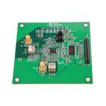
The MAX1420 evaluation kit (EV kit) is a fully assembled
and tested circuit board that contains all the components necessary to evaluate the performance of the
MAX1420, MAX1421, or MAX1422, 12-bit, +3.3V, analog-to-digital converters (ADCs). The MAX1420/
MAX1421/MAX1422 ADCs accept 2Vp-p differential
analog inputs. The offset binary digital output produced
by the ADC can be easily sampled with a user-provided
high-speed logic analyzer or data-acquisition system.
The EV kit comes with the 60Msps part (MAX1420)
installed. Order a free sample of the MAX1421CCM or
MAX1422CCM to evaluate the 40Msps or 20Msps parts.
�MAX1420 Evaluation Kit
Evaluates: MAX1420/MAX1421/MAX1422
Component List (continued)
DESIGNATION
QTY
R19, R20, R24,
R25
4
DESCRIPTION
Quick Start
• DC power supplies
Digital (+3.3V, 100mA)
10kΩ ±5%, 0805 resistors
Analog (+3.3V, 100mA)
• Function generator with low-phase noise and lowjitter for clock input (e.g., HP 8662A or equivalent)
R21, R22, R26,
R27
4
24.9Ω ±1%, 0805 resistors
R41
1
820Ω ±1%, 0805 resistor
R42
1
620Ω ±1%, 0805 resistor
• Function generator for analog signal input (e.g., HP
8662A or equivalent)
R43
0
Resistor not installed
(short PC trace)
• Logic analyzer or data-acquisition system (e.g., HP
1663EP, HP 16500C or equivalent)
T1, T2
2
RF transformers
Mini-Circuits T1-1T-KK81
Coilcraft WB2010-1-SM
• Bandpass filter selected for the input frequency of
interest (e.g., TTE Q56 series or equivalent)
U1
1
MAX1420CCM, 48-pin TQFP
1
16-bit buffer/driver three-state
output, 48-pin TSSOP
IDT 74ALVC16244APA
Texas Instruments
SN74ALVCH16244ADGGR
U2
The MAX1420 EV kit is fully assembled and tested.
Follow the steps below to verify board operation.
Do not turn on the power supply until all connections are completed.
1) Verify that the shunts are installed in the following
positions:
JU1 (2-3)
JU2 (2-3)
2) Connect the clock function generator to the CLKIN
SMA connector.
Component Suppliers
SUPPLIER
Coilcraft
PHONE
847-639-6400
FAX
847-639-1469
4) Connect the output of the filter to the analog input
SMA connector (VIN) of the MAX1420 EV kit.
Fair-Rite Products
888-324-7748
888-337-7483
IDT
800-345-7015
408-492-8674
5) Connect the logic analyzer to the square pin header
(J1), where D11 is the MSB and D0 is the LSB.
Mini-Circuits
718-934-4500
718-934-7092
Murata
814-237-1431
814-238-0490
Taiyo Yuden
408-573-4150
408-573-4159
TDK
847-803-6100
847-803-6296
7) Connect a +3.3V power supply to DVDD1. Connect
the ground terminal of this supply to DGND.
Texas Instruments
972-644-5580
214-480-7800
8) Turn on both power supplies.
Part Selection Table
2
3) Connect the output of the analog signal function generator to the input of the bandpass filter.
PART
SPEED (Msps)
MAX1420CCM
60
MAX1421CCM
40
MAX1422CCM
20
6) Connect a +3.3V power supply to AVDD and VS+.
Connect the ground terminal of this supply to AGND.
9) Enable the function generators. Set the clock function generator to 2Vp-p and frequency ≤ 60MHz. Set
the analog signal function generator to 2Vp-p and the
desired frequency. The function generators should
be phase locked to ensure optimum performance.
10) Set the logic analyzer to capture data on the rising
edge of the clock.
11) Collect and evaluate the data using the logic
analyzer.
_______________________________________________________________________________________
�MAX1420 Evaluation Kit
The MAX1420 EV kit is a fully assembled and tested
circuit board that contains all the components necessary to evaluate the performance of the MAX1420,
MAX1421, or MAX1422, 12-bit ADC at a maximum
clock frequency of 60MHz. The EV kit is designed
using a four-layer architecture, to optimize the performance of the MAX1420. Separate, nonoverlapping,
analog and digital power planes minimize noise coupling between analog and digital signals.
For simple operation, the EV kit is specified to have
+3.3V power supplies applied to analog and digital
power planes. However, the digital supply can be operated down to +2.7V without compromising the board’s
performance. The logic analyzer’s threshold should be
adjusted accordingly.
Access to the digital outputs and the capture clock is
provided through connector J1. The 26-pin connector
interfaces directly to a user-provided logic analyzer or
data-acquisition system.
Power Supplies
The MAX1420 EV kit requires separate analog and digital power supplies for best performance. A +3.3V
power supply is used to power the analog portion
(AVDD) of the MAX1420/MAX1421/MAX1422. A second
separate +3.3V power supply is used to power the digital portion (DVDD1) of the MAX1420 and the buffer/driver, but it will work with a supply as low as +2.7V and
as high as +3.6V. Enhanced dynamic performance can
be achieved when the digital supply voltage is lower
than the analog supply voltage.
Input Signal
The MAX1420 EV kit requires a single-ended analog
input signal. This single-ended signal is converted to a
differential signal by transformer T1. This differential
Table 1. Jumper JU1 and JU2 Functions
JUMPER
JU1
SHUNT
LOCATION
FUNCTION
1-2
MAX1420 in power-down
mode
2-3
MAX1420 operational
1-2
Digital outputs D0–D11
disabled (high impedance)
2-3
Digital outputs D0–D11
enabled
signal is applied to the input pins (INP and INN) of the
MAX1420. Both input pins receive half of the input signal swing applied at the SMA connector VIN centered
at (VS+/2).
MAX1420 Enable and Power-Down
The MAX1420 EV kit features jumpers to enable and
power-down the MAX1420 (JU1) or enable/disable its
digital outputs (JU2). See Table 1 for jumper settings.
Voltage Reference
The MAX1420 requires a voltage reference to set the
full-scale analog input range. The MAX1420 provides
three modes of operation to set the reference voltage.
In internal reference mode, the on-chip +2.048V
bandgap reference is used. The pads CMLT, REFNT,
REFPT, and REFIN must be left floating in this mode. In
buffered external reference mode, a stable and accurate voltage must be applied at the REFIN pad to set
the reference voltage. The pads CMLT, REFNT, and
REFPT must be left floating in this mode. Connecting
REFIN to AGND activates the unbuffered external reference mode. In this mode, the full-scale input range is
determined by the voltage difference (VDIFF) between
the pads REFPT and REFNT. In this mode, CMLT must
be biased between +1.568V to +1.733V. REFPT and
REFNT should be biased to V CMLT + (V DIFF/2) and
VCMLT - (VDIFF/2), respectively.
Output Buffer/Driver
The 74ALVC16244 buffers the MAX1420’s digital outputs, and is able to drive capacitive loads without compromising the MAX1420’s dynamic performance. The
outputs of the buffer are connected to a 26-pin header
(J1) located on the right side of the EV kit, where the
user can connect a logic analyzer or data-acquisition
system.
Clock
The MAX1420 EV kit requires a single-ended sinusoidal
clock input signal. This single-ended signal is converted to a differential signal by transformer T2. The differential signal is then applied to the clock pins (CLK and
CLK) of the MAX1420. The clock frequency determines
the sampling rate of the MAX1420. The frequency
should be between 100kHz and 60MHz. The clock signal is also connected through the 74ALVC16244 to the
26-pin header J1, to be used by a logic analyzer or
data-acquisition system.
JU2
_______________________________________________________________________________________
3
Evaluates: MAX1420/MAX1421/MAX1422
Detailed Description
�VS+
C38
10µF
VIN
J2
C39
1µF
R18
49.9Ω
AGND
AVDD
C40
0.01µF
4
3
6
5
T1
C33
0.1µF
C31
0.1µF
AVDD
C7
0.1µF
C5
0.1µF
C41
0.22µF
R22
24.9Ω
R21
24.9Ω
C2
10µF
AVDD
2
1
R43
SHORT
(PC TRACE)
R20
10kΩ
5%
R19
10kΩ
5%
C53
1000pF
C1
1µF
C36
OPEN
C35
22pF
NOTES:
1. ALL RESISTORS ARE 1% UNLESS OTHERWISE SPECIFIED.
C8
1000pF
C6
1000pF
C37
OPEN
C34
1000pF
C32
1000pF
12
11
10
9
8
7
6
5
4
3
2
1
13
L2
AVDD
L3
AVDD
C10
0.1µF
14
C9
1000pF
AGND
AGND
AVDD
AVDD
AGND
AGND
INN
INP
AGND
AGND
AVDD
AVDD
AVDD
AVDD
AGND
AGND
47
48
C30
1000pF
C29
0.1µF
AVDD
CLK
C43
22pF
1
R23
49.9Ω
2
C42
1000pF
T2
6
R27
24.9Ω
C47
0.22µF
C14
0.1µF
3
AVDD
19
20
C45
C13
22pF 1000pF
AGND
5
4
18
U1
REFIN
43
C22
1000pF
C21
0.22µF
REFIN
MAX1420
C24
1000pF
REFP
44
C48
0.22µF
CLK
17
C44
22pF
R26
24.9Ω
R25
10kΩ
5%
R24
10kΩ
5%
C12
0.22µF
C46
0.1µF
16
C11
1000pF
AVDD
15
C26
1000pF
REFN
45
AGND
C28
1000pF
C23
0.22µF
REFPT
R5
49.9Ω
C25
0.22µF
REFNT
R4
49.9Ω
C27
0.22µF
CML
46
R3
49.9Ω
CMLT
J3
CLKIN
C16
0.1µF
22
3
1
2
DVDD
PD
40
JU1
DGND
AGND
41
C15
1000pF
DVDD
21
DVDD
AVDD
42
C20
1000pF
C19
0.1µF
AVDD
D1
DVDD
CLKIN
B–DGND
25
26
27
28
30
31
32
33
34
35
C3
1µF
C17
1000pF
R7
100Ω
C58
1µF
24
D2
D3
D4
D5
DGND
DGND
DVDD
DVDD
D6
D7
D8
36
R6
100Ω
C4
10µF
C59
OPEN
D0
23
38 37
JU2
OE D11 D10
D9
39
3
1
2
DGND
DVDD1
C51
1000pF
R17
100Ω
R16
100Ω
R15
100Ω
R14
100Ω
R13
100Ω
R12
100Ω
C18
0.1µF
R11
100Ω
R10
100Ω
R9
100Ω
R8
100Ω
L1
C60
OPEN
C54
1µF
C52
1µF
DVD
R1
10Ω
5%
3OE
3A3
3A4
4A1
4A2
47
46
44
43
41
40
38
1A1
1A3
1A3
1A4
2A1
2A2
2A3
28
GND
34
GND
39
GND
35
3A2
36
3A1
37
2A4
45
GND
46
2OE
25
33
32
30
29
4A3
26 4A4
27
DVD
16
17
19
20
22
GND
1OE
GND
GND
GND
4OE
1Y1
1Y2
1Y3
1Y4
2Y1
2Y2
1
4
21
10
24
15
2
3
5
6
8
9
14
3Y2
13
3Y1
12
2Y4
11
2Y3
3Y3
3Y4
4Y1
4Y2
4Y3
7
VCC
18
VCC
42
VCC
31
VCC
23
4Y4
J1–26
C50
0.1µF
J1–1
J1–3
J1–5
J1–7
J1–9
J1–11
J1–13
B–DGND
J1–2
J1–4
J1–6
J1–8
J1–10
J1–12
J1–14
J1–16
J1–18
J1–20
J1–22
J1–15 J1–24
J1–17
J1–19
J1–21
J1–23
J1–25
C49
2200pF
B–DGND
R40
49.9Ω
R39
49.9Ω
R38
49.9Ω
R37
49.9Ω
R36
49.9Ω
R35
49.9Ω
R34
49.9Ω
R33
49.9Ω
R32
49.9Ω
R31
49.9Ω
R30
49.9Ω
R29
49.9Ω
R28
49.9Ω
DVD
B–DGND
JU3
U2
74ALVCH16244A
C55 R2
OPEN 10Ω
5%
B–DGND
R42
620Ω
R41
820Ω
B–DGND
DVDD
B–DGND
C56
0.22µF
C57
OPEN
Evaluates: MAX1420/MAX1421/MAX1422
MAX1420 Evaluation Kit
Figure 1. MAX1420 EV Kit Schematic
4_______________________________________________________________________________________________________
_______________________________________________________________________________________
4
�MAX1420 Evaluation Kit
Figure 3. MAX1420 EV Kit PC Board Layout—Component Side
Figure 4. MAX1420 EV Kit PC Board Layout—Solder Side
Figure 5. MAX1420 EV Kit Component Placement Guide—
Solder Side
_______________________________________________________________________________________
5
Evaluates: MAX1420/MAX1421/MAX1422
Figure 2. MAX1420 EV Kit Component Placement Guide—
Component Side
�Evaluates: MAX1420/MAX1421/MAX1422
MAX1420 Evaluation Kit
Figure 6. MAX1420 EV Kit PC Board Layout—Inner GND Layer
Figure 7. MAX1420 EV Kit PC Board Layout—Inner VCC Layer
Maxim cannot assume responsibility for use of any circuitry other than circuitry entirely embodied in a Maxim product. No circuit patent licenses are
implied. Maxim reserves the right to change the circuitry and specifications without notice at any time.
6 _____________________Maxim Integrated Products, 120 San Gabriel Drive, Sunnyvale, CA 94086 408-737-7600
© 2001 Maxim Integrated Products
Printed USA
is a registered trademark of Maxim Integrated Products.
�


 工商网监
湘ICP备2023018690号
工商网监
湘ICP备2023018690号
