19-3433; Rev 0; 10/04
15-Bit, 80Msps ADC with -78.4dBFS
Noise Floor for IF Applications
The MAX1428 is a 5V, high-speed, high-performance
analog-to-digital converter (ADC) featuring a fully differential wideband track-and-hold (T/H) and a 15-bit converter core. The MAX1428 is optimized for multichannel,
multimode receivers, which require the ADC to meet very
stringent dynamic performance requirements. With a
noise floor of -78.4dBFS, the MAX1428 allows for the
design of receivers with superior sensitivity.
The MAX1428 achieves two-tone, spurious-free dynamic
range (SFDR) of -82dBc for input tones of 69MHz and
71MHz. Its excellent signal-to-noise ratio (SNR) of 73.9dB
and single-tone SFDR performance (SFDR1/SFDR2) of
83dBc/91dBc at fIN = 70MHz and a sampling rate of
80Msps make this part ideal for high-performance digital
receivers.
The MAX1428 operates from an analog 5V and a digital
3V supply, features a 2.56VP-P full-scale input range,
and allows for a sampling speed of up to 80Msps. The
input T/H operates with a -1dB full-power bandwidth of
260MHz.
The MAX1428 features parallel, CMOS-compatible outputs in two’s-complement format. To enable the interface
with a wide range of logic devices, this ADC provides a
separate output driver power-supply range of 2.3V to
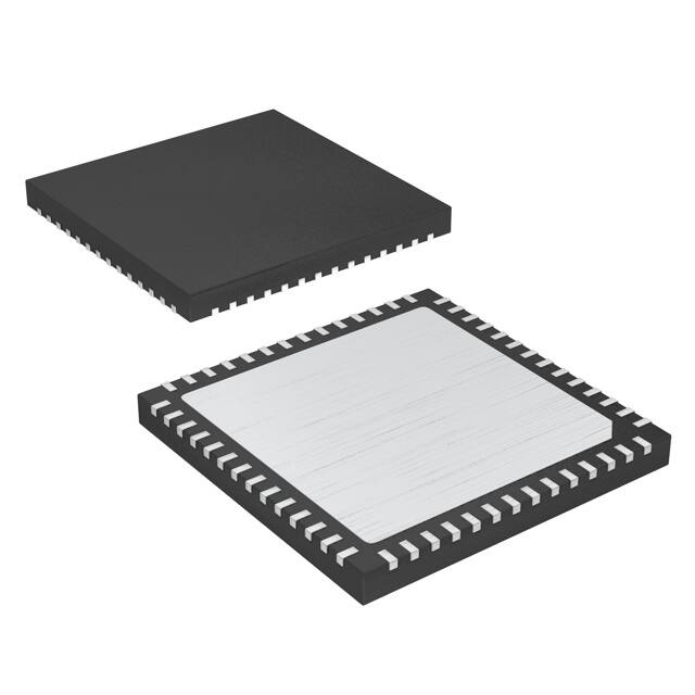
3.5V. The MAX1428 is manufactured in an 8mm x 8mm,
56-pin thin QFN package with exposed paddle (EP) for
low thermal resistance, and is specified for the extended
industrial (-40°C to +85°C) temperature range.
Note that IF parts MAX1418, MAX1428, and MAX1430
(see Pin-Compatible Higher/Lower Speed Versions
Selection table) are recommended for applications that
require high dynamic performance for input frequencies greater than fCLK/3. Unlike its baseband counterpart MAX1427, the MAX1428 is optimized for input
frequencies greater than fCLK/3.
Applications
Features
♦ 80Msps Minimum Sampling Rate
♦ -78.4dBFS Noise Floor
♦ Excellent Dynamic Performance
73.9dB SNR at fIN = 70MHz and AIN = -2dBFS
83dBc/91dBc Single-Tone SFDR1/SFDR2 at
fIN = 70MHz and AIN = -2dBFS
-82dB Multitone SFDR at fIN1 = 69MHz
and fIN2 = 71MHz
♦ Less than 0.25ps Sampling Jitter
♦ Fully Differential Analog Input Voltage Range of
2.56VP-P
♦ CMOS-Compatible Two’s-Complement Data Output
♦ Separate Data Valid Clock and Overrange Outputs
♦ Flexible-Input Clock Buffer
♦ EV Kit Available for MAX1428
(Order MAX1427EVKIT)
Ordering Information
PART
MAX1428ETN
PIN-PACKAGE
56 Thin QFN-EP*
*EP = Exposed paddle.
Pin-Compatible Higher/Lower
Speed Versions Selection
Cellular Base-Station Transceiver Systems (BTS)
Wireless Local Loop (WLL)
TEMP RANGE
-40°C to +85°C
PART
SPEED GRADE
(Msps)
TARGET
APPLICATION
Single- and Multicarrier Receivers
MAX1418
65
IF
Multistandard Receivers
MAX1419
65
Baseband
E911 Location Receivers
MAX1427
80
Baseband
Power Amplifier Linearity Correction
MAX1428
80
IF
Antenna Array Processing
MAX1429
100
Baseband
MAX1430
100
IF
Pin Configuration appears at end of data sheet.
________________________________________________________________ Maxim Integrated Products
For pricing, delivery, and ordering information, please contact Maxim/Dallas Direct! at
1-888-629-4642, or visit Maxim’s website at www.maxim-ic.com.
1
MAX1428
General Description
�MAX1428
15-Bit, 80Msps ADC with -78.4dBFS
Noise Floor for IF Applications
ABSOLUTE MAXIMUM RATINGS
AVCC, DVCC, DRVCC to GND.................................. -0.3V to +6V
INP, INN, CLKP, CLKN, CM to GND........-0.3V to (AVCC + 0.3V)
D0–D14, DAV, DOR to GND..................-0.3V to (DRVCC + 0.3V)
Continuous Power Dissipation (TA = +70°C)
56-Pin Thin QFN (derate 47.6mW/°C above +70°C) ...3809.5mW
Operating Temperature Range ...........................-40°C to +85°C
Thermal Resistance θJA ...................................................21°C/W
Junction Temperature ......................................................+150°C
Storage Temperature Range .............................-60°C to +150°C
Lead Temperature (soldering, 10s) .................................+300°C
Stresses beyond those listed under “Absolute Maximum Ratings” may cause permanent damage to the device. These are stress ratings only, and functional
operation of the device at these or any other conditions beyond those indicated in the operational sections of the specifications is not implied. Exposure to
absolute maximum rating conditions for extended periods may affect device reliability.
ELECTRICAL CHARACTERISTICS
(AVCC = 5V, DVCC = DRVCC = 2.5V, GND = 0, INP and INN driven differentially with -2dBFS, CLKP and CLKN driven differentially
with a 2VP-P sinusoidal input signal, CL = 5pF at digital outputs, fCLK = 80MHz, TA = TMIN to TMAX, unless otherwise noted. Typical
values are at TA = +25°C, unless otherwise noted. ≥+25°C guaranteed by production test,
很抱歉,暂时无法提供与“MAX1428ETN+TD”相匹配的价格&库存,您可以联系我们找货
免费人工找货