MAX14750 Evaluation Kit
General Description
The MAX14750 evaluation kit (EV kit) is a fully assembled
and tested circuit for evaluating the MAX14720/MAX14750
power-management solutions with I2C capability for
space-constrained, battery-powered applications. Both the
MAX14720 and MAX14750 integrate a synchronous buck
converter, a buck-boost converter, a linear regulator, and
a power switch. The MAX14750 provides individual pin
enables for each function, while the MAX14720 includes
a push-button monitor and sequencing controller. Refer to
the MAX14720/MAX14750 IC data sheet for detailed information regarding the operation and features of the devices.
The EV kit comes standard with the MAX14750A installed,
but can also be used to evaluate the MAX14720 by replacing
the MAX14750A (U1) with the MAX14720. Request a free
sample of the MAX14720 when ordering the EV kit.
Evaluates: MAX14720/MAX14750
Detailed Description of Hardware
The MAX14750 evaluation kit (EV Kit) evaluates the
MAX14720/MAX14750 compact power management
solutions.
See Table 1 thru Table 3 for pin description of the three
connectors J1–J3.
Hardware Modification
Resistors R1 and R4–R9 are uninstalled by default. VCC
can be used to power the inputs of the four major blocks
(LIN, BIN, HVIN, and SWIN) by populating R1, R5, R7,
and R9 accordingly. The blocks can also be cascaded in
any order by selectively populating R4, R6, R7, and R9.
The EV kit hardware is configured by default for the
evaluation of the MAX14750. To evaluate the MAX14720,
remove R2 and install a short at R3.
Features
●● RoHS Compliant
●● Proven PCB Layout
●● Full Assembled and Tested
●● I2C Serial Interface
19-8661; Rev 0; 10/16
Ordering Information appears at end of data sheet.
�MAX14750 Evaluation Kit
Table 1. Connector J1
PIN
Evaluates: MAX14720/MAX14750
Table 2. Connector J2
PIN
SIGNAL
1
MAX14720 MAX14750
GND
GND
Ground
DESCRIPTION
1
LIN
LDO Input
2
MON
MON
Monitor Multiplexer Output
2
BIN
Buck Regulator Input
3
N.C.
N.C.
Not Connected
4
N.C.
N.C.
Not Connected
3
HVIN
Buck-Boost Regulator Input (Must be
connected to HVIN)
5
RST
N.C.
(MAX14720) Reset Output.
(MAX14750) Not Connected
4
SWIN
Power Switch Input
5
LOUT
LDO Output
6
SDA
SDA
I2C Serial Data Input/Output
6
BOUT
Buck Regulator Output
7
HVOUT
Buck-Boost Regulator Output
8
SWOUT
Power Switch Output
7
SCL
SCL
I2C
8
N.C.
LEN
(MAX14720) Not Connected
(MAX14750) Linear
Regulator Enable Input
BEN
(MAX14720) Multi-purpose
Control Input (MAX14750)
Buck Regulator Enable
9
MPC
KOUT
10
Serial Clock Input
HVEN
(MAX14720) Key Output
(MAX14750) Buck-boost
Regulator Enable Input
(MAX14720) Key Input
(MAX14750) Power Switch
Enable Input
11
KIN
SWEN
12
GND
GND
Ground
DESCRIPTION
Table 3. Connector J3
PIN
SIGNAL
DESCRIPTION
1
GND
Ground
2
N.C.
Not Connected
3
N.C.
Not Connected
4
VCC
Chip Power Input
5
N.C.
Not Connected
6
CAP
Internal Power Decoupling
7
N.C.
Not Connected
8
N.C.
Not Connected
9
N.C.
Not Connected
10
N.C.
Not Connected
11
N.C.
Not Connected
12
GND
Ground
Component Suppliers
SUPPLIER
WEBSITE
Murata Americas
www.murata.com
TDK Corp
www.component.tdk.com
Bourns
www.bourns.com
Note: Indicate that you are using the MAX14750 when contacting these component suppliers.
Ordering Information
PART
TYPE
MAX14750EVKIT#
EV Kit
#Denotes RoHS compliant.
www.maximintegrated.com
Maxim Integrated │ 2
�MAX14750 Evaluation Kit
Evaluates: MAX14720/MAX14750
MAX14750 EV System Bill of Materials
ITEM
REF_DES
DNI/DNP QTY
MFG PART #
MANUFACTURER
VALUE
DESCRIPTION
COMMENTS
1
C1-C3, C11
-
4
C1608X5R0J226M080AC
TDK
22µF
CAPACITOR; SMT (0603);
CERAMIC CHIP; 22µF; 6.3V;
TOL=20%; MODEL=C SERIES;
TG=-55°C TO +85°C; TC=X5R
2
C4, C5, C8
-
3
C1005X5R1A475M050BC
TDK
4.7µF
CAPACITOR; SMT (0402);
CERAMIC CHIP; 4.7µF; 10V;
TOL=20%; MODEL=C SERIES;
TG=-55°C TO +85°C; TC=X5R
3
C6, C7
-
2
C1005X5R1H104K050
TDK
0.1µF
CAPACITOR; SMT (0402);
CERAMIC CHIP; 0.1µF; 50V;
TOL=10%; MODEL=C SERIES;
TG=-55°C TO +85°C; TC=X5R;
4
C9
-
1
C3216X5R1A107M
TDK
100µF
CAPACITOR; SMT (1206);
CERAMIC CHIP; 100µF; 10V;
TOL=20%; MODEL=C SERIES;
TG=-55°C TO +85°C; TC=X5R
5
J1, J3
-
2
90120-0772
MOLEX
90120-0772
CONNECTOR; THROUGH HOLE;
C-GRID III SINGLE ROW STRAIGHT
PIN HEADER; GOLD PLATED CONTACT;
STRAIGHT THROUGH; 12PINS
6
J2
-
1
90120-0768
MOLEX
90120-0768
CONNECTOR; THROUGH HOLE;
C-GRID III SINGLE ROW STRAIGHT
PIN HEADER; GOLD PLATED CONTACT;
STRAIGHT THROUGH; 8PINS
7
L1
-
1
VLS201610ET-4R7M
TDK
4.7µH
INDUCTOR; SMT; WIREWOUND CHIP;
4.7µH; TOL=±20%; 0.72A
8
L2
-
1
SRP2010-2R2M
BOURNS
2.2µH
INDUCTOR; SMT; POWDERED
IRON CORE; 2.2µH; TOL=±20%;
1.7A
9
R10, R11
-
2
CRCW040210K0FK;
RC0402FR-0710K
VISHAY DALE;
YAGEO PHICOMP
10K
RESISTOR; 0402; 10K; 1%; 100PPM;
0.0625W; THICK FILM
10
R1, R3, R4-R9
DNP
0
N/A
N/A
OPEN
PACKAGE OUTLINE 0402 RESISTOR
SAMSUNG
ELECTRONICS/
BOURNS/YAGEO PH
11
R2
-
0
RC1608J000CS;
CR0603-J/-000ELF;
RC0603JR-070RL
12
U1
-
1
MAX14750AEWA+
MAXIM
IC; MAX14750A; 25 WLP;
MAX14750AEWA+ PACKAGE CODE W252M2+1;
21-0788
13
PCB
-
1
MAX14720
MAXIM
PCB
www.maximintegrated.com
0
RESISTOR; 0603; 0 OHM; 5%; JUMPER;
0.10W; THICK FILM
PCB Board:MAX14720 EVALUATION KIT
Maxim Integrated │ 3
�GND
GPIO4
GPIO3
GPIO1
GPIO2
SCL
SDA
RST#
12
11
10
9
8
7
6
IN
IN
IN
IN
IN
IN
GPIO4
GPIO3
GPIO1
GPIO2
SCL
SDA
RST#
RST#
GPIO2
IN
SWIN
4
IN
IN
LIN
3
5
IN
MON
BIN
IN
2
IN
IN
R2
VCC
R1
OPEN
R3
IN
GPIO3
0
R4
J2
SWIN
HVILX
HVOLX
PFN1
PFN2
PFN4
PFN3
B5
E3
E2
D3
E5
D4
C4
R7
OPEN
R8
OPEN
CAP
SDA
SCL
MON
SWOUT
LOUT
BOUT
BLX
R9
OPEN
D5
C1
D1
B1
C5
A5
A3
A2
IN
SDA
IN
C7
0.1UF
50V
SCL
IN
C9
100UF
10V
C8
4.7UF
10V
C3
22UF
6.3V
1
C2
22UF
6.3V
CAP
R10
2.2UH
L2
10K
2
V1
1%
10K
1%
R11
V7
V6
3
V5
4
V4
5
V3
6
V2
7
8
2
R6
LIN
A4
OPEN
BIN
A1
E1
1
V8
R5
OPEN
GPIO1
IN
IN
1
GPIO4
4.7UH
L1
OPEN
OPEN
2
C5
4.7UF
10V
C4
4.7UF
10V
C1
22UF
6.3V
HVOUT
LIN
IN
MON
HVIN
E4
BIN
IN
C11
22UF
6.3V
HVIN
IN
IN
U1
MAX147X0
SWIN
IN
HVIN
VCC
LOUT
IN
1
VCC
B4
BOUT
IN
GND
J1
50V
0.1UF
GND
B2
GND
C6
GND
B3
HVOUT
IN
C2
GND
C3
GND
D2
SWOUT
www.maximintegrated.com
IN
HVOUT
BOUT
LOUT
SWOUT
MON
IN
IN
IN
IN
IN
CAP
IN
VCC
12
11
10
9
8
7
6
5
4
3
2
1
J3
GND
CAP
VCC
GND
MAX14750 Evaluation Kit
Evaluates: MAX14720/MAX14750
MAX14750 EV System Schematic
Maxim Integrated │ 4
�MAX14750 Evaluation Kit
Evaluates: MAX14720/MAX14750
MAX14750 EV System PCB Layout
MAX14720/MAX14750 EV—Top Silkscreen
MAX14720/MAX14750 EV—Top
MAX14720/MAX14750 EV—Internal 2
www.maximintegrated.com
Maxim Integrated │ 5
�MAX14750 Evaluation Kit
Evaluates: MAX14720/MAX14750
MAX14750 EV System PCB Layout (continued)
MAX14720/MAX14750 EV—Internal 3
MAX14720/MAX14750 EV—Bottom
MAX14720/MAX14750 EV—Bottom Silkscreen
www.maximintegrated.com
Maxim Integrated │ 6
�MAX14750 Evaluation Kit
Evaluates: MAX14720/MAX14750
Revision History
REVISION
NUMBER
REVISION
DATE
0
10/16
DESCRIPTION
Initial release
PAGES
CHANGED
—
For pricing, delivery, and ordering information, please contact Maxim Direct at 1-888-629-4642, or visit Maxim Integrated’s website at www.maximintegrated.com.
Maxim Integrated cannot assume responsibility for use of any circuitry other than circuitry entirely embodied in a Maxim Integrated product. No circuit patent licenses
are implied. Maxim Integrated reserves the right to change the circuitry and specifications without notice at any time.
Maxim Integrated and the Maxim Integrated logo are trademarks of Maxim Integrated Products, Inc.
© 2016 Maxim Integrated Products, Inc. │ 7
�
很抱歉,暂时无法提供与“MAX14750EVKIT#”相匹配的价格&库存,您可以联系我们找货
免费人工找货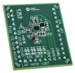


 工商网监
湘ICP备2023018690号
工商网监
湘ICP备2023018690号
