EVALUATION KIT AVAILABLE
MAX17043/MAX17044
1-Cell/2-Cell Fuel Gauge with
ModelGauge and Low-Battery Alert
General Description
Features
The MAX17043/MAX17044 are ultra-compact, low-cost,
host-side fuel-gauge systems for lithium-ion (Li+) batteries in handheld and portable equipment. The MAX17043
is configured to operate with a single lithium cell and the
MAX17044 is configured for a dual-cell 2S pack.
The MAX17043/MAX17044 use a sophisticated Li+ battery-modeling scheme, called ModelGauge™ to track
the battery’s relative state-of-charge (SOC) continuously
over a widely varying charge/discharge profile. Unlike
traditional fuel gauges, the ModelGauge algorithm eliminates the need for battery relearn cycles and an external
current-sense resistor. Temperature compensation is possible in the application with minimal interaction between a
μC and the device.
The IC can be located on the system side, reducing cost
and supply chain constraints on the battery. Measurement
and estimated capacity data sets are accessed through
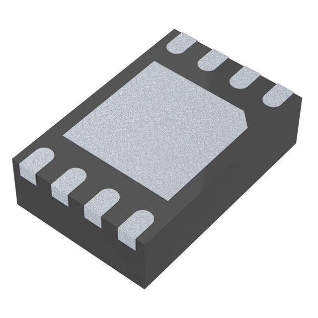
an I2C interface. The MAX17043/MAX17044 are available in either a 0.4mm pitch 9-bump UCSP™ or 2mm x
3mm, 8-pin TDFN lead-free package.
●● Host-Side or Battery-Side Fuel Gauging
• 1 Cell (MAX17043)
• 2 Cell (MAX17044)
●● Precision Voltage Measurement
• ±12.5mV Accuracy to 5.00V (MAX17043)
• ±30mV Accuracy to 10.00V (MAX17044)
●● Accurate Relative Capacity (RSOC) Calculated from
ModelGauge Algorithm
●● No Offset Accumulation on Measurement
●● No Full-to-Empty Battery Relearning Necessary
●● No Sense Resistor Required
●● External Alarm/Interrupt for Low-Battery Warning
●● 2-Wire Interface
●● Low Power Consumption
●● Tiny, Lead(Pb)-Free, 8-Pin, 2mm x 3mm TDFN
Package or Tiny 0.4mm Pitch 9-Bump UCSP Package
Ordering Information
PART
MAX17043G+U
MAX17043G+T
MAX17043X+
MAX17043X+T10
MAX17044G+U
MAX17044G+T
MAX17044X+
MAX17044X+T10
Applications
●●
●●
●●
●●
●●
●●
Smartphones, Tablets
Health and Fitness Monitors
Digital Still, Video, and Action Cameras
Medical Devices
Handheld Computers and Terminals
Wireless Speakers
ModelGauge is a trademark of Maxim Integrated Products, Inc.
UCSP is a trademark of Maxim Integrated Products, Inc.
Simple Fuel-Gauge Circuit Diagram
150Ω
1kΩ
CELL
ALRT
19-4811; Rev 7; 1/17
4.7kΩ
SYSTEM
µP
VDD
INTERRUPT
MAX17043
MAX17044
1µF
PIN-PACKAGE
8 TDFN-EP*
8 TDFN-EP*
9 UCSP
9 UCSP
8 TDFN-EP*
8 TDFN-EP*
9 UCSP
9 UCSP
+Denotes a lead(Pb)-free/RoHS-compliant package.
T = Tape and reel.
*EP = Exposed pad.
Visit www.maximintegrated.com/products/patents for product
patent marking information.
Li+
PROTECTION
CIRCUIT
TEMP RANGE
-20°C to +70°C
-20°C to +70°C
-20°C to +70°C
-20°C to +70°C
-20°C to +70°C
-20°C to +70°C
-20°C to +70°C
-20°C to +70°C
QSTRT
CTG
SDA
GND
SCL
EP
I2C BUS
MASTER
10nF
�1-Cell/2-Cell Fuel Gauge with
ModelGauge and Low-Battery Alert
MAX17043/MAX17044
Absolute Maximum Ratings
Voltage on CTG Pin Relative to VGND....................-0.3V to +12V
Voltage on CELL Pin Relative to VGND..................-0.3V to +12V
Voltage on All Other Pins Relative to VGND..............-0.3V to +6V
Operating Temperature Range..............................-40°C to +85°C
Storage Temperature Range
(TA = 0°C to +70°C (Note 10)).......................-55°C to +125°C
Lead Temperature (TDFN soldering only, 10s) ...............+300°C
Soldering Temperature (reflow) .......................................+260°C
Stresses beyond those listed under “Absolute Maximum Ratings” may cause permanent damage to the device. These are stress ratings only, and functional operation of the device at these
or any other conditions beyond those indicated in the operational sections of the specifications is not implied. Exposure to absolute maximum rating conditions for extended periods may affect
device reliability.
Electrical Characteristics Recommended DC Operating Conditions
(2.5V ≤ VDD ≤ 4.5V, TA = -20°C to +70°C, unless otherwise noted.)
PARAMETER
Supply Voltage
Data I/O Pins
SYMBOL
VDD
CONDITIONS
MIN
TYP
MAX
UNITS
(Note 1)
+2.5
+4.5
V
SCL, SDA,
QSTRT, (Note 1)
ALRT
-0.3
+5.5
V
MAX17043 CELL Pin
VCELL
(Note 1)
-0.3
+5.0
V
MAX17044 CELL Pin
VCELL
(Note 1)
-0.3
+10.0
V
TYP
MAX
UNITS
50
75
µA
0.5
1.0
1
3
DC Electrical Characteristics
(2.5V ≤ VDD ≤ 4.5V, TA = -20°C to +70°C, unless otherwise noted. Contact Maxim for VDD greater than 4.5V.)
PARAMETER
SYMBOL
Active Current
IACTIVE
Sleep-Mode Current (Note 2)
ISLEEP
Time-Base Accuracy
MAX17043 VoltageMeasurement Error
MAX17044 VoltageMeasurement Error
CELL Pin Input Impedance
tERR
CONDITIONS
VDD = 2.0V
VDD = 3.6V at +25°C
-1
+1
TA = 0°C to +70°C (Note 10)
-2
+2
TA = -20°C to +70°C
-3
+3
-12.5
+12.5
-30
+30
TA = +25°C, 5.0V < VIN < 9.0V
-30
+30
5.0 < VIN < 9.0
-60
+60
TA = +25°C, VIN = VDD
VGERR
MIN
RCELL
µA
%
mV
mV
15
MΩ
1.4
V
Input Logic-High:
SCL, SDA, QSTRT
VIH
(Note 1)
Input Logic-Low:
SCL, SDA, QSTRT
VIL
(Note 1)
0.5
V
Output Logic-Low: SDA
VOL
IOL = 4mA (Note 1)
0.4
V
Output Logic-Low: ALRT
VOL-ALRT
IOL-ALRT = 2mA (Note 1)
IPD
VDD = 4.5V, VPIN = 0.4V
Pulldown Current: SCL, SDA
Input Capacitance: SCL, SDA
CBUS
Bus Low Timeout
tSLEEP
(Note 3)
Mode Transition
tTRAN
(Note 4)
www.maximintegrated.com
0.4
0.2
1.75
V
µA
50
pF
2.5
s
1
ms
Maxim Integrated │ 2
�1-Cell/2-Cell Fuel Gauge with
ModelGauge and Low-Battery Alert
MAX17043/MAX17044
Electrical Characteristics: 2-Wire Interface
(2.5V ≤ VDD ≤ 4.5V, TA = -20°C to +70°C, unless otherwise noted.)
PARAMETER
SYMBOL
SCL Clock Frequency
fSCL
Bus Free Time Between a STOP
and START Condition
tBUF
Hold Time (Repeated)
START Condition
tHD:STA
CONDITIONS
(Note 5)
(Note 5)
MIN
0
TYP
MAX
UNITS
400
kHz
1.3
µs
0.6
µs
Low Period of SCL Clock
tLOW
1.3
µs
High Period of SCL Clock
tHIGH
0.6
µs
Setup Time for a Repeated
START Condition
tSU:STA
0.6
µs
Data Hold Time
tHD:DAT
(Notes 6, 7)
Data Setup Time
tSU:DAT
(Note 6)
0
0.9
100
µs
ns
Rise Time of Both SDA
and SCL Signals
tR
20 +
0.1CB
300
ns
Fall Time of Both SDA
and SCL Signals
tF
20 +
0.1CB
300
ns
Setup Time for STOP Condition
tSU:STO
0.6
Spike Pulse Widths Suppressed
by Input Filter
tSP
(Note 8)
Capacitive Load for Each
Bus Line
CB
(Note 9)
SCL, SDA Input Capacitance
CBIN
0
µs
50
ns
400
pF
60
pF
Note
Note
Note
Note
Note
Note
Note
1: All voltages are referenced to GND.
2: SDA, SCL = GND; QSTRT, ALRT idle.
3: The MAX17043/MAX17044 enter Sleep mode 1.75s to 2.5s after (SCL < VIL) AND (SDA < VIL).
4: Time to enter sleep after Sleep command is sent. Time to exit sleep on rising edge of SCL or SDA.
5: fSCL must meet the minimum clock low time plus the rise/fall times.
6: The maximum tHD:DAT has only to be met if the device does not stretch the low period (tLOW) of the SCL signal.
7: This device internally provides a hold time of at least 75ns for the SDA signal (referred to the VIHMIN of the SCL signal) to
bridge the undefined region of the falling edge of SCL.
Note 8: Filters on SDA and SCL suppress noise spikes at the input buffers and delay the sampling instant.
Note 9: CB—total capacitance of one bus line in pF.
Note 10: Applies to 8-pin TDFN-EP package type only.
www.maximintegrated.com
Maxim Integrated │ 3
�1-Cell/2-Cell Fuel Gauge with
ModelGauge and Low-Battery Alert
QUIESCENT CURRENT
vs. SUPPLY VOLTAGE
TA = +70°C
60
40
20
TA = -20°C
80
0
1
2
3
60
2
50
0
40
-2
30
-4
20
4
0
5
-6
REFERENCE SOC:
SOLID LINE
0
2
4
MAX17043/4 toc03
MAX17043/
MAX17044 SOC:
DASHED LINE
10
20
8
15
70
4
60
2
50
0
40
-2
30
-4
20
REFERENCE SOC:
SOLID LINE
10
0
0
2
4
6
VOLTAGE ADC ERROR (mV)
6
SOC ERROR (%)
STATE OF CHARGE (%)
80
ERROR (%)
6
8
10
-8
12
-10
TIME (h)
SIMPLE C/4 RATE CYCLES*
SOC ACCURACY
90
6
4
VDD (V)
100
8
70
10
0
10
-6
ERROR (%)
VCELL = 4.2V
10
VCELL = 3.0V
5
0
-5
VCELL = 3.6V
-10
-15
-8
8 10 12 14 16 18 20 22
MAX17043 VOLTAGE ADC ERROR
vs. TEMPERATURE
MAX17043/4 toc04
TA = +25°C
MAX17043/
MAX17044 SOC:
DASHED LINE
90
STATE OF CHARGE (%)
QUIESCENT CURRENT (µA)
80
MAX17043/4 toc02
100
MAX17043/4 toc01
100
SIMPLE C/2 RATE CYCLES*
SOC ACCURACY
SOC ERROR (%)
MAX17043/MAX17044
-20
-10
-40
-15
10
35
60
85
TEMPERATURE (°C)
TIME (hr)
C/2 RATE ZIGZAG PATTERN*
SOC ACCURACY
MAX17043/4 toc05
MAX17043/MAX17044 SOC:
DASHED LINE
STATE OF CHARGE (%)
90
80
8
6
ERROR (%)
70
10
4
60
2
50
0
40
-2
30
-4
20
0
-6
REFERENCE SOC:
SOLID LINE
10
0
4
8
SOC ERROR (%)
100
-8
12
16
20
22
-10
TIME (hr)
* Sample accuracy with custom configuration data programmed into the IC.
www.maximintegrated.com
Maxim Integrated │ 4
�1-Cell/2-Cell Fuel Gauge with
ModelGauge and Low-Battery Alert
MAX17043/MAX17044
Pin Configurations
TOP VIEW
SDA SCL QSTRT ALRT
8
7
6
5
TOP VIEW
(BUMPS ON BOTTOM)
MAX17043
MAX17044
1
2
3
A
SDA
SCL
CTG
B
QSTRT
N.C.
CELL
C
ALRT
VDD
GND
+
MAX17043
MAX17044
+
1
2
3
4
CTG CELL VDD GND
TDFN
(2mm x 3mm)
UCSP
Pin Description
PIN
NAME
FUNCTION
UCSP
TDFN
A1
8
SDA
Serial Data Input/Output. Open-drain 2-wire data line. Connect this pin to the DATA signal of the
2-wire interface. This pin has a 0.2µA typical pulldown to sense disconnection.
A2
7
SCL
Serial Clock Input. Input only 2-wire clock line. Connect this pin to the CLOCK signal of the 2-wire
interface. This pin has a 0.2µA typical pulldown to sense disconnection.
A3
1
CTG
Connect to Ground. Connect to VSS during normal operation.
B1
6
QSTRT
N.C.
No connect. Do not connect.
B3
2
CELL
Battery Voltage Input. The voltage of the cell pack is measured through this pin.
C1
5
ALRT
Alert Output. Active-low interrupt signaling low state of charge. Connect to interrupt input of the
system microprocessor.
C2
3
VDD
Power-Supply Input. 2.5V to 4.5V input range. Connect to system power through a decoupling
network. Connect a 10nF typical decoupling capacitor close to pin.
C3
4
GND
Ground. Connect to the negative power rail of the system.
—
—
EP
B2
www.maximintegrated.com
Quick-Start Input. Allows reset of the device through hardware. Connect to GND if not used.
Exposed Pad (TDFN only). Connect to ground.
Maxim Integrated │ 5
�1-Cell/2-Cell Fuel Gauge with
ModelGauge and Low-Battery Alert
MAX17043/MAX17044
SDA
tF
tLOW
tSU:DAT
tR
tSP
tF
tR
tBUF
tHD:STA
SCL
tHD:STA
S
tSU:STA
tHD:DAT
tSU:STO
Sr
P
S
Figure 1. 2-Wire Bus Timing Diagram
Detailed Description
Figure 1 shows the 2-wire bus timing diagram, and
Figure 2 is the MAX17043/MAX17044 block diagram.
ModelGauge Theory of Operation
The MAX17043/MAX17044 use a sophisticated battery
model that determines the SOC of a nonlinear Li+ battery.
The model effectively simulates the internal dynamics of a
Li+ battery and determines the SOC. The model considers the time effects of a battery caused by the chemical
reactions and impedance in the battery. The MAX17043/
MAX17044 SOC calculation does not accumulate error
with time. This is advantageous compared to traditional
MAX17043
MAX17044
VDD
BIAS
VOLTAGE
REFERENCE
ADC (VCELL)
CELL
GND
IC
GROUND
Figure 2. Block Diagram
www.maximintegrated.com
TIME BASE
(32kHz)
STATE
MACHINE
(SOC, RATE)
CTG
2-WIRE
INTERFACE
SDA
QSTRT
ALRT
SCL
coulomb counters, which suffer from SOC drift caused by
current-sense offset and cell self-discharge. This model
provides good performance for many Li+ chemistry variants across temperature and age. To achieve optimum
performance, the MAX17043/MAX17044 must be programmed with configuration data custom to the application. Contact the factory for details.
Fuel-Gauge Performance
The classical coulomb-counter-based fuel gauges suffer
from accuracy drift due to the accumulation of the offset
error in the current-sense measurement. Although the
error is often very small, the error increases over time in
such systems, cannot be eliminated, and requires periodic corrections. The corrections are usually performed
on a predefined SOC level near full or empty. Some other
systems use the relaxed battery voltage to perform corrections. These systems determine the true SOC based
on the battery voltage after a long time of no activity. Both
have the same limitation: if the correction condition is not
observed over time in the actual application, the error in
the system is boundless. In some systems, a full-charge/
discharge cycle is required to eliminate the drift error. To
determine the true accuracy of a fuel gauge, as experienced by end users, the battery should be exercised
in a dynamic manner. The end-user accuracy cannot
be understood with only simple cycles. MAX17043/
MAX17044 do not suffer from the drift problem since they
do not rely on the current information.
Maxim Integrated │ 6
�1-Cell/2-Cell Fuel Gauge with
ModelGauge and Low-Battery Alert
MAX17043/MAX17044
IC Power-Up
When the battery is first inserted into the system, there is
no previous knowledge about the battery’s SOC. The IC
assumes that the battery has been in a relaxed state for
the previous 30min. The first A/D voltage measurement is
translated into a best “first guess” for the SOC. Initial error
caused by the battery not being in a relaxed state fades
over time, regardless of cell loading following this initial
conversion. Because the SOC determination is convergent rather than divergent (as in a coulomb counter), this
initial error does not have a longlasting impact.
Quick-Start
A quick-start allows the MAX17043/MAX17044 to restart
fuel-gauge calculations in the same manner as initial power-up of the IC. For example, if an application’s power-up
sequence is exceedingly noisy such that excess error
is introduced into the IC’s “first guess” of SOC, the host
can issue a quick-start to reduce the error. A quick-start
is initiated by a rising edge on the QSTRT pin, or through
software by writing 4000h to the MODE register.
ALERT Interrupt
The MAX17043/MAX17044 have an interrupt feature that
alerts a host microprocessor whenever the cell’s state of
charge, as defined by the SOC register, falls below a predefined alert threshold set at address 0Dh of the CONFIG
register.
When an alert is triggered, the IC drives the ALRT pin to
logic-low and sets the ALRT bit in the CONFIG register
to logic 1. The ALRT pin remains logic-low until the host
software writes the ALRT bit to logic 0 to clear the interrupt. Clearing the ALRT bit while SOC is below the alert
threshold does not generate another interrupt. The SOC
register must first rise above and then fall below the alert
threshold value before another interrupt is generated.
Note that the alert function is not disabled at IC powerup.
If the first SOC calculation is below the threshold setting,
an interrupt is generated. Entering Sleep mode does not
clear the interrupt.
Sleep Mode
Holding both SDA and SCL logic-low forces the MAX17043/
MAX17044 into Sleep mode. While in Sleep mode, all IC
operations are halted and power drain of the IC is greatly
reduced. After exiting Sleep mode, fuel-gauge operation
continues from the point it was halted. SDA and SCL must
be held low for at least 2.5s to guarantee transition into
Sleep mode. Afterwards, a rising edge on either SDA or
SCL immediately transitions the IC out of Sleep mode.
Alternatively, Sleep mode can be entered by setting the
SLEEP bit in the CONFIG register to logic 1 through I2C
communication. If the SLEEP bit is set to logic 1, the only
way to exit Sleep mode is to write SLEEP to logic 0 or
power-on reset the IC.
Power-On Reset (POR)
Writing a value of 0054h to the COMMAND register
causes the MAX17043/MAX17044 to completely reset as
if power had been removed. The reset occurs when the
last bit has been clocked in. The IC does not respond with
an I2C ACK after this command sequence.
Registers
All host interaction with the MAX17043/MAX17044 is handled by writing to and reading from register locations. The
MAX17043/MAX17044 have six 16-bit registers: SOC,
VCELL, MODE, VERSION, CONFIG, and COMMAND.
Register reads and writes are only valid if all 16 bits are
transferred. Any write command that is terminated early
is ignored. The function of each register is described
as follows. All remaining address locations not listed in
Table 1 are reserved. Data read from reserved locations
is undefined.
Table 1. Register Summary
ADDRESS
(HEX)
REGISTER
02h–03h
VCELL
04h–05h
SOC
06h–07h
MODE
08h–09h
VERSION
0Ch–0Dh
CONFIG
FEh–FFh
COMMAND
www.maximintegrated.com
READ/
WRITE
DEFAULT
(HEX)
Reports 12-bit A/D measurement of battery voltage.
R
—
Reports 16-bit SOC result calculated by ModelGauge algorithm.
R
—
Sends special commands to the IC.
W
—
Returns IC version.
R
—
R/W
971Ch
W
—
DESCRIPTION
Battery compensation. Adjusts IC performance based on
application conditions.
Sends special commands to the IC.
Maxim Integrated │ 7
�1-Cell/2-Cell Fuel Gauge with
ModelGauge and Low-Battery Alert
MAX17043/MAX17044
VCELL Register
Battery voltage is measured at the CELL pin input
with respect to GND over a 0 to 5.00V range for the
MAX17043 and 0 to 10.00V for the MAX17044 with
resolutions of 1.25mV and 2.50mV, respectively. The A/D
calculates the average cell voltage for a period of 125ms
after IC POR and then for a period of 500ms for every
cycle afterwards. The VCELL register requires 500ms to
update after exiting Sleep mode. The result is placed in
the VCELL register at the end of each conversion period.
Figure 3 shows the VCELL register format.
Table 2. MODE Register Commands
VALUE
COMMAND
4000h
Quick-Start
The SOC register is a read-only register that displays
the state of charge of the cell as calculated by the
ModelGauge algorithm. The result is displayed as a
percentage of the cell’s full capacity. This register automatically adapts to variation in battery size since the
MAX17043/MAX17044 naturally recognize relative SOC.
Units of % can be directly determined by observing only
the high byte of the SOC register. The low byte provides
additional resolution in units 1/256%. The reported SOC
also includes residual capacity, which might not be available to the actual application because of early termination
voltage requirements. When SOC() = 0, typical applications have no remaining capacity.
The first update occurs within 250ms after POR of the IC.
Subsequent updates occur at variable intervals depending
on application conditions. ModelGauge calculations outside the register are clamped at minimum and maximum
register limits. Figure 4 shows the SOC register format.
MODE Register
The MODE register allows the host processor to send
special commands to the IC (Table 2). Valid MODE register write values are listed as follows. All other MODE
register values are reserved.
The VERSION register is a read-only register that contains a value indicating the production version of the
MAX17043/MAX17044.
CONFIG Register
The CONFIG register compensates the ModelGauge
algorithm, controls the alert interrupt feature, and forces
the IC into Sleep mode through software. The format of
CONFIG is shown in Figure 5.
CONFIG
CONFIG is an 8-bit value that can be adjusted to optimize
IC performance for different lithium chemistries or different operating temperatures. Contact Maxim for instructions for optimization. The power-up default value for
CONFIG is 97h.
MSB—ADDRESS 02h
210
See the Quick-Start
description section.
VERSION Register
SOC Register
211
DESCRIPTION
29
28
27
26
LSB—ADDRESS 03h
25
MSB
24
23
LSB
MSB
22
21
20
0
0
0
0
LSB
0: BITS ALWAYS READ LOGIC 0
UNITS: 1.25mV FOR MAX17043
2.50mV FOR MAX17044
Figure 3. VCELL Register Format
MSB—ADDRESS 04h
27
26
25
24
MSB
23
22
LSB—ADDRESS 05h
21
20
2-1
LSB
MSB
2-2
2-3
2-4
2-5
2-6
2-7
2-8
LSB
UNITS: 1.0%
Figure 4. SOC Register Format
www.maximintegrated.com
Maxim Integrated │ 8
�1-Cell/2-Cell Fuel Gauge with
ModelGauge and Low-Battery Alert
MAX17043/MAX17044
MSB—ADDRESS 0Ch
LSB—ADDRESS 0Dh
RCOMP RCOMP RCOMP RCOMP RCOMP RCOMP RCOMP RCOMP
27
26
25
24
23
22
21
20
MSB
LSB
SLEEP X
ALRT
ATHD ATHD ATHD ATHD ATHD
24
23
22
21
20
MSB
LSB
ATHD UNITS: 1 LSB = 2’S COMPLEMENT 1%
ATHD RANGE: 11111b = 1%
00000b = 32%
Figure 5. CONFIG Register Format
SLEEP (Sleep Bit)
Writing SLEEP to logic 1 forces the ICs into Sleep mode.
Writing SLEEP to logic 0 forces the ICs to exit Sleep
mode. The power-up default value for SLEEP is logic 0.
ATHD (Alert Threshold)
This bit reads as either a logic 0 or logic 1. This bit cannot
be written.
The alert threshold is a 5-bit value that sets the state of
charge level where an interrupt is generated on the ALRT
pin. The alert threshold has an LSb weight of 1% and can
be programmed from 1% up to 32%. The threshold value
is stored in two’s-complement form (00000 = 32%, 00001
= 31%, 00010 = 30%, 11111 = 1%). The power-up default
value for ATHD is 4% or 1Ch.
ALRT (ALERT Flag)
COMMAND Register
X (Don’t Care)
This bit is set by the IC when the SOC register value
falls below the alert threshold setting and an interrupt is
generated. This bit can only be cleared by software. The
power-up default value for ALRT is logic 0.
Table 3. COMMAND Register Commands
VALUE
COMMAND
0054h
POR
DESCRIPTION
The COMMAND register allows the host processor to
send special commands to the IC. Valid COMMAND
register write values are listed as follows. All other
COMMAND register values are reserved. Table 3 shows
COMMAND register commands.
Application Examples
The MAX17043/MAX17044 have a variety of configurations, depending on the application. Table 4 shows the
most common system configurations and the proper pin
connections for each.
See the Power-On Reset
(POR) section.
Table 4. Possible Application Configurations
SYSTEM CONFIGURATION
IC
VDD
ALRT
QSTRT
1S Pack-Side Location
MAX17043
Power directly from battery
Leave unconnected
Connect to GND
1S Host-Side Location
MAX17043
Power directly from battery
Leave unconnected
Connect to GND
Connect to GND
1S Host-Side Location,
Low Cell Interrupt
MAX17043
Power directly from battery
Connect to system
interrupt
1S Host-Side Location,
Hardware Quick-Start
MAX17043
Power directly from battery
Leave unconnected
Connect to rising-edge
reset signal
2S Pack-Side Location
MAX17044
Power from +2.5V to +4.5V
LDO in pack
Leave unconnected
Connect to GND
2S Host-Side Location
MAX17044
Power from +2.5V to +4.5V
LDO or PMIC
Leave unconnected
Connect to GND
2S Host-Side Location,
Low Cell Interrupt
MAX17044
Power from +2.5V to +4.5V
LDO or PMIC
Connect to system
interrupt
Connect to GND
2S Host-Side Location,
Hardware Quick-Start
MAX17044
Power from +2.5V to +4.5V
LDO or PMIC
Leave unconnected
Connect to rising-edge
reset signal
www.maximintegrated.com
Maxim Integrated │ 9
�1-Cell/2-Cell Fuel Gauge with
ModelGauge and Low-Battery Alert
MAX17043/MAX17044
BATTERY
SYSTEM
SYSTEM VDD
PACK+
150Ω
1kΩ
4.7kΩ
SYSTEM µP
CELL
VDD
INTERRUPT
INPUT
ALRT
MAX17043
PROTECTION IC
(Li+/POLYMER)
1µF
QSTRT
CTG
SDA
GND
SCL
EP
I2C BUS
MASTER
10nF
SYSTEM GND
PACK-
Figure 6. MAX17043 Application Example with Alert Interrupt
BATTERY
SYSTEM
SYSTEM VDD
PACK+
1kΩ
SYSTEM PMIC
CELL
VDD
QSTRT
3.3V OUTPUT
WATCHDOG
MAX17044
PROTECTION IC
(Li+/POLYMER)
1µF
ALRT
SDA
CTG
SCL
GND
PACK-
EP
I2C BUS
MASTER
SYSTEM µP
SYSTEM GND
Figure 7. MAX17044 Application Example with Hardware Reset
Figure 6 shows an example application for a 1S cell pack.
The MAX17043 is mounted on the system side and powered directly from the cell pack. The external RC networks
on VDD and CELL provide noise filtering of the IC power
supply and A/D measurement. In this example, the ALRT
pin is connected to the microprocessor’s interrupt input
to allow the MAX17043 to signal when the battery is low.
The QSTRT pin is unused in this application, so it is tied
to GND.
www.maximintegrated.com
Figure 7 shows a MAX17044 example application using
a 2S cell pack. The MAX17044 is mounted on the system side and powered from a 3.3V supply generated
by the system. The CELL pin is still connected directly
to PACK+ through an external noise filter. The ALRT
pin is left unconnected because the interrupt feature is
not used in this application. After power is supplied, the
system watchdog generates a low-to-high transition on
the QSTRT pin to signal the MAX17044 to perform a
quick-start.
Maxim Integrated │ 10
�MAX17043/MAX17044
2-Wire Bus System
The 2-wire bus system supports operation as a slave-only
device in a single or multislave, and single or multimaster
system. Slave devices can share the bus by uniquely
setting the 7-bit slave address. The 2-wire interface
consists of a serial-data line (SDA) and serialclock line
(SCL). SDA and SCL provide bidirectional communication
between the MAX17043/MAX17044 slave device and a
master device at speeds up to 400kHz. The MAX17043/
MAX17044s’ SDA pin operates bidirectionally; that is,
when the MAX17043/MAX17044 receive data, SDA operates as an input, and when the MAX17043/MAX17044
return data, SDA operates as an open-drain output,
with the host system providing a resistive pullup. The
MAX17043/MAX17044 always operate as a slave device,
receiving and transmitting data under the control of a
master device. The master initiates all transactions on the
bus and generates the SCL signal, as well as the START
and STOP bits, which begin and end each transaction.
Bit Transfer
One data bit is transferred during each SCL clock cycle,
with the cycle defined by SCL transitioning low-to-high
and then high-to-low. The SDA logic level must remain
stable during the high period of the SCL clock pulse.
Any change in SDA when SCL is high is interpreted as a
START or STOP control signal.
Bus Idle
The bus is defined to be idle, or not busy, when no master
device has control. Both SDA and SCL remain high when
the bus is idle. The STOP condition is the proper method
to return the bus to the idle state.
START and STOP Conditions
The master initiates transactions with a START condition
(S) by forcing a high-to-low transition on SDA while SCL
is high. The master terminates a transaction with a STOP
condition (P), a low-to-high transition on SDA while SCL
is high. A Repeated START condition (Sr) can be used in
place of a STOP then START sequence to terminate one
transaction and begin another without returning the bus to
the idle state. In multimaster systems, a Repeated START
allows the master to retain control of the bus. The START
and STOP conditions are the only bus activities in which
the SDA transitions when SCL is high.
www.maximintegrated.com
1-Cell/2-Cell Fuel Gauge with
ModelGauge and Low-Battery Alert
Acknowledge Bits
Each byte of a data transfer is acknowledged with an
acknowledge bit (A) or a no-acknowledge bit (N). Both
the master and the MAX17043 slave generate acknowledge bits. To generate an acknowledge, the receiving
device must pull SDA low before the rising edge of the
acknowledge-related clock pulse (ninth pulse) and keep it
low until SCL returns low. To generate a no-acknowledge
(also called NAK), the receiver releases SDA before the
rising edge of the acknowledge-related clock pulse and
leaves SDA high until SCL returns low. Monitoring the
acknowledge bits allows for detection of unsuccessful
data transfers. An unsuccessful data transfer can occur
if a receiving device is busy or if a system fault has
occurred. In the event of an unsuccessful data transfer,
the bus master should reattempt communication.
Data Order
A byte of data consists of 8 bits ordered most significant
bit (MSb) first. The least significant bit (LSb) of each
byte is followed by the acknowledge bit. The MAX17043/
MAX17044 registers composed of multibyte values are
ordered MSb first. The MSb of multibyte registers is
stored on even data-memory addresses.
Slave Address
A bus master initiates communication with a slave device
by issuing a START condition followed by a slave address
(SAddr) and the read/write (R/W) bit. When the bus is
idle, the MAX17043/MAX17044 continuously monitor for
a START condition followed by its slave address. When
the MAX17043/MAX17044 receive a slave address that
matches the value in the slave address register, they
respond with an acknowledge bit during the clock period
following the R/W bit. The 7-bit slave address is fixed to
6Ch (write)/6Dh (read):
MAX17043/MAX17044
SLAVE ADDRESS
0110110
Read/Write Bit
The R/W bit following the slave address determines the
data direction of subsequent bytes in the transfer. R/W = 0
selects a write transaction, with the following bytes being
written by the master to the slave. R/W = 1 selects a read
transaction, with the following bytes being read from the
slave by the master. (Table 5).
Maxim Integrated │ 11
�1-Cell/2-Cell Fuel Gauge with
ModelGauge and Low-Battery Alert
MAX17043/MAX17044
Table 5. 2-Wire Protocol Key
KEY
DESCRIPTION
KEY
DESCRIPTION
S
START bit
Sr
Repeated START
SAddr
Slave address (7 bit)
W
R/W bit = 0
MAddr
Memory address byte
P
STOP bit
Data
Data byte written by master
Data
Data byte returned by slave
A
Acknowledge bit—master
A
Acknowledge bit—slave
N
No acknowledge—master
N
No acknowledge—slave
Bus Timing
The MAX17043/MAX17044 are compatible with any bus
timing up to 400kHz. No special configuration is required
to operate at any speed.
2-Wire Command Protocols
The command protocols involve several transaction formats. The simplest format consists of the master writing
the START bit, slave address, R/W bit, and then monitoring the acknowledge bit for presence of the MAX17043/
MAX17044. More complex formats, such as the Write
Data and Read Data, read data and execute devicespecific operations. All bytes in each command format
require the slave or host to return an acknowledge bit
before continuing with the next byte. Table 5 shows the
key that applies to the transaction formats.
Basic Transaction Formats
Write: S. SAddr W. A. MAddr. A. Data0. A. Data1. A. P
A write transaction transfers 2 or more data bytes to the
MAX17043/MAX17044. The data transfer begins at the
memory address supplied in the MAddr byte. Control of
the SDA signal is retained by the master throughout the
transaction, except for the acknowledge cycles:
Read: S. SAddr W. A. MAddr. A. Sr. SAddr R. A. Data0. A. Data1. N. P
Write Portion
Read Portion
A read transaction transfers 2 or more bytes from the
MAX17043/MAX17044. Read transactions are composed
of two parts, a write portion followed by a read portion,
and are therefore inherently longer than a write transaction. The write portion communicates the starting point
for the read operation. The read portion follows immediately, beginning with a Repeated START, slave address
www.maximintegrated.com
with R/W set to a 1. Control of SDA is assumed by the
MAX17043/MAX17044, beginning with the slave address
acknowledge cycle. Control of the SDA signal is retained
by the MAX17043/MAX17044 throughout the transaction,
except for the acknowledge cycles. The master indicates
the end of a read transaction by responding to the last
byte it requires with a no acknowledge. This signals the
MAX17043/MAX17044 that control of SDA is to remain
with the master following the acknowledge clock.
Write Data Protocol
The write data protocol is used to write to register to
the MAX17043/MAX17044 starting at memory address
MAddr. Data0 represents the data written to MAddr, Data1
represents the data written to MAddr + 1, and DataN
represents the last data byte, written to MAddr + N. The
master indicates the end of a write transaction by sending a STOP or Repeated START after receiving the last
acknowledge bit:
SAddr W. A. MAddr. A. Data0. A. Data1. A... DataN. A.
The MSB of the data to be stored at address MAddr can
be written immediately after the MAddr byte is acknowledged. Because the address is automatically incremented
after the LSB of each byte is received by the MAX17043/
MAX17044, the MSB of the data at address MAddr + 1
can be written immediately after the acknowledgment of
the data at address MAddr. If the bus master continues an
autoincremented write transaction beyond address 4Fh,
the MAX17043/MAX17044 ignore the data. A valid write
must include both register bytes. Data is also ignored
on writes to read-only addresses. Incomplete bytes and
bytes that are not acknowledged by the MAX17043/
MAX17044 are not written to memory.
Maxim Integrated │ 12
�1-Cell/2-Cell Fuel Gauge with
ModelGauge and Low-Battery Alert
MAX17043/MAX17044
Read Data Protocol
The read data protocol is used to read to register from the
MAX17043/MAX17044 starting at the memory address
specified by MAddr. Both register bytes must be read
in the same transaction for the register data to be valid.
Data0 represents the data byte in memory location
MAddr, Data1 represents the data from MAddr + 1, and
DataN represents the last byte read by the master:
S. SAddr W. A. MAddr. A. Sr. SAddr R. A.
Data0. A. Data1. A... DataN. N. P
Data is returned beginning with the MSB of the data in
MAddr. Because the address is automatically incremented after the LSB of each byte is returned, the MSB of the
data at address MAddr + 1 is available to the host immediately after the acknowledgment of the data at address
MAddr. If the bus master continues to read beyond
address FFh, the MAX17043/MAX17044 output data values of FFh. Addresses labeled Reserved in the memory
map return undefined data. The bus master terminates
the read transaction at any byte boundary by issuing a no
acknowledge followed by a STOP or Repeated START.
Package Information
For the latest package outline information and land patterns (footprints), go to www.maximintegrated.com/packages. Note that a “+”,
“#”, or “-” in the package code indicates RoHS status only. Package drawings may show a different suffix character, but the drawing
pertains to the package regardless of RoHS status.
PACKAGE TYPE
PACKAGE CODE
OUTLINE NO.
LAND PATTERN NO.
8 TDFN
T823+1
21-0174
90-0091
9 UCSP
W91C1+1
21-0459
Refer to
Application Note 1891
www.maximintegrated.com
Maxim Integrated │ 13
�1-Cell/2-Cell Fuel Gauge with
ModelGauge and Low-Battery Alert
MAX17043/MAX17044
Revision History
REVISION
NUMBER
REVISION
DATE
PAGES
CHANGED
0
9/09
Initial release
1
4/10
Updated soldering temperature information; updated CTG pin voltage range to from 0.3V
to +12V to -0.3V to +12V in Absolute Maximum Ratings section; removed future asterisks
in ordering table; changed update time for SOC and VCELL; changed registers from
110ms/440ms to 125ms/500ms
2
9/10
Added description and ordering information for UCSP package type
1, 2, 3, 5,
13, 14
3
10/10
Updated Ordering Information table
1, 2, 13,14
4
8/11
Corrected time from start up until SOC valid; added text indicating accurate results require
custom configuration for each application
4, 6, 8, 14
5
6/12
Corrected soldering temperature in Absolute Maximum Ratings
6
8/12
Changed Soft POR command from 5400h to 0054h to avoid possible memory corruption
7
1/17
Updated front page title and applications
DESCRIPTION
—
1, 2, 8
2
7, 9, 14
1
For pricing, delivery, and ordering information, please contact Maxim Direct at 1-888-629-4642, or visit Maxim Integrated’s website at www.maximintegrated.com.
Maxim Integrated cannot assume responsibility for use of any circuitry other than circuitry entirely embodied in a Maxim Integrated product. No circuit patent licenses
are implied. Maxim Integrated reserves the right to change the circuitry and specifications without notice at any time. The parametric values (min and max limits)
shown in the Electrical Characteristics table are guaranteed. Other parametric values quoted in this data sheet are provided for guidance.
Maxim Integrated and the Maxim Integrated logo are trademarks of Maxim Integrated Products, Inc.
© 2017 Maxim Integrated Products, Inc. │ 14
�