EVALUATION KIT AVAILABLE
4A, Low-Noise, High-Frequency,
Step-Up DC-DC Converter
MAX1709
General Description
Benefits and Features
The MAX1709 sets a new standard of space savings
for high-power, step-up DC-DC conversion. It delivers
up to 20W at a fixed (3.3V or 5V) or adjustable (2.5V to
5.5V) output, using an on-chip power MOSFET from a
+0.7V to +5V supply.
Fixed-frequency PWM operation ensures that the
switching noise spectrum is constrained to the 600kHz
fundamental and its harmonics, allowing easy postfiltering for noise reduction. External clock synchronization
capability allows for even tighter noise spectrum control. Quiescent power consumption is less than 1mW to
extend operating time in battery-powered systems.
Two control inputs (ONA, ONB) allow simple push-on,
push-off control through a single momentary pushbutton switch, as well as conventional on/off logic control.
The MAX1709 also features programmable soft-start
and current limit for design flexibility and optimum performance with batteries.
• Integration Reduces External Component Count to
Save Space
• On-Chip 10A Power MOSFET
• 5V, 4A Output from a 3.3V Input
• Fixed 3.3V or 5V Output Voltage or
Adjustable (2.5V to 5.5V)
• Input Voltage Range Down to 0.7V
• Constant Frequency Reduces Post-Filtering
• Low-Noise, Constant-Frequency Operation
(600kHz)
• Synchronizable Switching Frequency
(350kHz to 1000kHz)
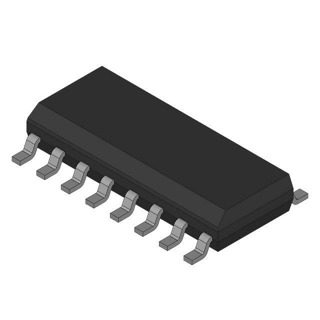
The MAX1709 is supplied in both a high-power TSSOP
package, which allows a 10ARMS switch current and a
4A output, and a narrow SO package, which supplies a
2.4A output with a switch rated at 6ARMS. Although the
narrow SO device has a lower RMS switch rating, it has
the same peak switch current rating as the TSSOP
device, and so can supply 4A loads intermittently. If
loads of 2A or less are required, refer to the MAX1708.
Routers, Servers, Workstations, Card Racks
Local 2.5V to 3.3V or 5V Conversion
Local 3.3V to 5V Conversion
3.6V or 5V RF PAs in Communications Handsets
Typical Operating Circuit
1µH
SYNC
OR
INTERNAL
CLK
LX
MAX1709
GND
SS/LIM
REF
PART
TEMP RANGE
-40°C to +85°C
16 Narrow SO
MAX1709EUI+
-40°C to +85°C
28 TSSOP-EP*
+Denotes a lead(Pb)-free/RoHS-compliant package.
*EP = Exposed pad.
OUT
TOP VIEW
ONA 1
28 ONB
LX 2
27 CLK
LX 3
OUTPUT
3.3V, 5V,
OR ADJ
UP TO 4A
26 3.3/5
MAX1709
25 NC
LX 5
24 NC
LX 6
23 PGND
LX 7
22 PGND
LX 8
21 PGND
NC 9
20 PGND
NC 10
19 PGND
GND 11
18 PGND
SS/ILM 12
17 NC
REF 13
16 FB
GND 14
15 OUT
TSSOP-EP
19-1724; Rev 3; 2/15
PIN-PACKAGE
MAX1709ESE
LX 4
INPUT
1V TO 5V
ONA
Ordering Information
Pin Configuration
Applications
OFF ON
• Lower Power Consumption Extends Battery Life
• 1mW Quiescent Power
�4A, Low-Noise, High-Frequency,
Step-Up DC-DC Converter
MAX1709
Absolute Maximum Ratings
ONA, ONB, OUT, SS/LIM, 3.3/5 to GND ...............-0.3V to +6.0V
LX to PGND ...........................................................-0.3V to +6.0V
FB, CLK, REF to GND.............................. -0.3V to (VOUT + 0.3V)
PGND to GND .......................................................-0.3V to +0.3V
Continuous Power Dissipation (TA = +70°C)
16-Pin Narrow SO (derate 16.5mW/°C above +70°C) .....1.3W
28-Pin TSSOP Exposed Pad
(derate 23.8mW/°C above +70°C) ...................................1.9W
28-Pin TSSOP Exposed Pad Junction-to-Exposed
Pad Thermal Resistance ......................................……1.2°C/W
Operating Temperature Range ...........................-40°C to +85°C
Junction Temperature ......................................................+150°C
Storage Temperature Range .............................-65°C to +150°C
Lead Temperature (soldering, 10s) .................................+300°C
Stresses beyond those listed under “Absolute Maximum Ratings” may cause permanent damage to the device. These are stress ratings only, and functional
operation of the device at these or any other conditions beyond those indicated in the operational sections of the specifications is not implied. Exposure to
absolute maximum rating conditions for extended periods may affect device reliability.
Electrical Characteristics
(VOUT = VCLK = +3.6V, ONA = ONB = FB = GND, TA = 0°C to +85°C, unless otherwise noted. Typical values are at TA = +25°C.)
PARAMETER
CONDITIONS
3.26
3.34
3.42
5.05
5.17
-0.25
-0.45
1.240
1.265
V
1
200
nA
5.5
V
Measured between 1A < ISW < 3A (Note 2)
ISW = 1A
UNITS
4.92
Load Regulation
VFB = +1.5V
MAX
3.3/5 = GND, ISW = 1A
VFB < 0.1V (Note 1)
FB Input Current
TYP
3.3/5 = OUT, ISW = 1A
Output Voltage
FB Regulation Voltage
MIN
Output Voltage Adjust Range
1.215
2.5
V
%/A
Output Undervoltage Lockout
(Note 3)
2.0
2.3
V
Frequency in Startup Mode
VOUT =1.5V
40
400
kHz
Minimum Startup Voltage
IOUT < 1mA (Note 1), TA = +25°C (Note 4)
1.1
V
Minimum Operating Voltage
(Note 5)
Soft-Start Pin Current
VSS/LIM = 1V
4
5.0
µA
OUT Supply Current
VFB = 1.5V (Note 6)
200
440
µA
V ONB = 3.6V
0.1
5
µA
VLX = V ONB = VOUT = +5.5V
0.1
40
µA
22
40
mΩ
OUT Leakage Current In
Shutdown
LX Leakage Current
n-Channel Switch
On-Resistance
n-Channel Current Limit
RMS Switch Current
0.7
3.2
SS/LIM = open
7.5
SS/LIM = 150kΩ to GND
3.5
V
9
12
5
6.5
MAX1709EUI+
10
MAX1709ESE
6
Reference Voltage
IREF = 0
Reference Load Regulation
-1µA < IREF < 50µA
Reference Supply Rejection
+2.5V < VOUT < +5.5V
1.245
A
ARMS
1.260
1.275
V
4
10
mV
0.2
5
mV
ONA, ONB, 3.3/5, 1.2V < VOUT < 5.5V
0.2 ×
VOUT
CLK, 2.7V < VOUT < 5.5V
0.2 ×
VOUT
Input Low Level (Note 7)
www.maximintegrated.com
0.9
V
Maxim Integrated | 2
�4A, Low-Noise, High-Frequency,
Step-Up DC-DC Converter
MAX1709
Electrical Characteristics (continued)
(VOUT = VCLK = +3.6V, ONA = ONB = FB = GND, TA = 0°C to +85°C, unless otherwise noted. Typical values are at TA = +25°C.)
PARAMETER
Input High Level
Logic Input Current
CONDITIONS
MIN
ONA, ONB, 3.3/5, 1.2V < VOUT
