19-1758; Rev 0; 8/00
High-Speed, Adjustable, Synchronous Step-Down
Controllers with Integrated Voltage Positioning
Features
♦ High-Efficiency Voltage Positioning
♦ Quick-PWM Architecture
♦ ±1% VOUT Line-Regulation Accuracy
♦ Adjustable Output Range (5-Bit DAC)
MAX1716: 0.925V to 1.6V
MAX1854: 0.925V to 2.0V
MAX1855: 0.600V to 1.75V
♦ 2V to 28V Input Range
♦ 200/300/400/550kHz Switching Frequency
♦ Output Undervoltage Protection
♦ Overvoltage Protection (MAX1716/MAX1855)
♦ Drive Large Synchronous-Rectifier MOSFETs
♦ 1.7ms Digital Soft-Start
♦ 700µA ICC Supply Current
♦ 1µA Shutdown Supply Current
♦ 2V ±1% Reference Output
♦ VGATE Transition-Complete Indicator
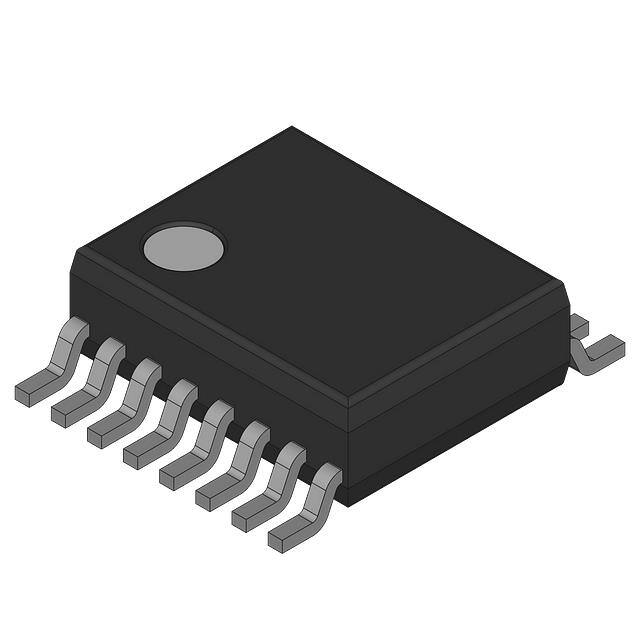
♦ Small 24-Pin QSOP Package
Typical Operating Circuit
________________________Applications
VCC
Notebook Computers
Docking Stations
CPU Core Supply
SHDN
VDD
V+
ILIM
BST
REF
DH
Two-Stage (+5V to VCORE) Converters
Ordering Information
GND
CS
TON
VPS
D0
TEMP. RANGE
PIN-PACKAGE
MAX1716EEG
-40°C to +85°C
24 QSOP
MAX1854EEG
-40°C to +85°C
24 QSOP
D3
MAX1855EEG
-40°C to +85°C
24 QSOP
D4
Quick-PWM is a trademark of Maxim Integrated Products.
SpeedStep is a trademark of Intel Corp.
OUTPUT
MAX1716
CC
MAX1854 LX
SKIP MAX1855 DL
Single-Stage (BATT to VCORE) Converters
PART
BATTERY
2V TO 28V
+5V INPUT
DAC
INPUTS
D1
PGND
D2
FB
VGATE
Pin Configuration appears at end of data sheet.
________________________________________________________________ Maxim Integrated Products
1
For free samples and the latest literature, visit www.maxim-ic.com or phone 1-800-998-8800.
For small orders, phone 1-800-835-8769.
MAX1716/MAX1854/MAX1855
General Description
The MAX1716/MAX1854/MAX1855 step-down controllers are intended for core CPU DC-DC converters in
notebook computers. They feature a dynamically
adjustable output (5-bit DAC), ultra-fast transient
response, high DC accuracy, and high efficiency needed for leading-edge CPU core power supplies. Maxim's
proprietary Quick-PWM™ quick-response, constant-ontime PWM control scheme handles wide input/output
voltage ratios with ease and provides 100ns “instant-on”
response to load transients while maintaining a relatively constant switching frequency.
The MAX1716/MAX1854/MAX1855 are designed
specifically for CPU core applications requiring a voltage-positioned supply. The voltage-positioning input
(VPS), combined with a high DC accuracy control loop,
is used to implement a power supply that modifies its
output set point in response to the load current. This
arrangement decreases full-load power dissipation and
reduces the required number of output capacitors.
The 28V input range of the MAX1716/MAX1854/MAX1855
enables single-stage buck conversion from high-voltage batteries for the maximum possible efficiency.
Alternatively, the devices’ high-frequency capability
combined with two-stage conversion (stepping down
the +5V system supply instead of the battery) allows
the smallest possible physical size. The output voltage
can be dynamically adjusted through the 5-bit digitalto-analog converter (DAC) inputs.
The MAX1716/MAX1854/MAX1855 are available in a
24-pin QSOP package. For applications requiring
SpeedStep™ power control (see the MAX1717).
�MAX1716/MAX1854/MAX1855
High-Speed, Adjustable, Synchronous Step-Down
Controllers with Integrated Voltage Positioning
ABSOLUTE MAXIMUM RATINGS
V+ to GND ..............................................................-0.3V to +30V
VCC, VDD to GND .....................................................-0.3V to +6V
PGND to GND.....................................................................±0.3V
SHDN, VGATE to GND .............................................-0.3V to +6V
ILIM, FB, CC, REF, D0–D4, VPS,
TON to GND ...........................................-0.3V to (VCC + 0.3V)
SKIP to GND (Note 1).................................-0.3V to (VCC + 0.3V)
DL to PGND................................................-0.3V to (VDD + 0.3V)
BST to GND ............................................................-0.3V to +36V
DH to LX ....................................................-0.3V to (VBST + 0.3V)
LX to BST..................................................................-6V to +0.3V
CS to GND.................................................................-2V to +30V
REF Short Circuit to GND ...........................................Continuous
Continuous Power Dissipation (TA = +70°C)
24-Pin QSOP (derate 9.5mW/°C above +70°C)...........762mW
Operating Temperature Range ...........................-40°C to +85°C
Junction Temperature ......................................................+150°C
Storage Temperature Range .............................-65°C to +150°C
Lead Temperature (soldering, 10s) .................................+300°C
Note 1: SKIP may be forced below -0.3V, temporarily exceeding the absolute maximum rating, for the purpose of debugging prototype breadboards, using the no-fault test mode. Limit the current drawn to -2mA (max).
Stresses beyond those listed under “Absolute Maximum Ratings” may cause permanent damage to the device. These are stress ratings only, and functional
operation of the device at these or any other conditions beyond those indicated in the operational sections of the specifications is not implied. Exposure to
absolute maximum rating conditions for extended periods may affect device reliability.
ELECTRICAL CHARACTERISTICS
(Circuit of Figure 1, V+ = +15V, VCC = VDD = 5V, SKIP = VCC, VPS = PGND, TA = 0°C to +85°C, unless otherwise noted. Typical
values are at TA = +25°C.)
PARAMETER
SYMBOL
CONDITIONS
MIN
TYP
MAX
UNITS
PWM CONTROLLER
Battery voltage, V+
Input Voltage Range
DC Output Voltage Accuracy
(Notes 2, 3)
V+ = 4.5V to 28V,
VPS = PGND
28
5.5
DAC codes from
1.35V to 2.0V
-1
1
DAC codes from
0.925V to 1.3V
-1.2
1.2
DAC codes from
0.6V to 0.9V
-1.5
1.5
-0.2
0.2
µA
-1
1
µA
0.197
%/mV
1
µA
100
nA
FB Input Bias Current
IFB
FB = 0.6V to 2.0V
VPS Input Bias Current
IVPS
VVPS = ±40mV
VPS Gain
AVPS
VVPS = 0 or -40mV, gain from VPS to FB
CS Input Bias Current
ICS
0 to 28V
ILIM Input Leakage Current
IILIM
VILIM = 0 or 5.0V
Soft-Start Ramp Time
On-Time (Note 4)
Minimum Off-Time (Note 4)
2
2
4.5
VCC, VDD
0.153
0.01
0 to full ILIM
tON
tOFF(MIN)
V+ = 11.0V,
VFB = 1.5V
0.175
-1
1.7
%
ms
TON = GND
205
255
300
TON = REF
280
327
375
TON = open
425
470
520
TON = VCC
615
678
740
400
500
_______________________________________________________________________________________
V
ns
ns
�High-Speed, Adjustable, Synchronous Step-Down
Controllers with Integrated Voltage Positioning
(Circuit of Figure 1, V+ = +15V, VCC = VDD = 5V, SKIP = VCC, VPS = PGND, TA = 0°C to +85°C, unless otherwise noted. Typical
values are at TA = +25°C.)
PARAMETER
SYMBOL
CONDITIONS
MIN
TYP
MAX
UNITS
BIAS AND REFERENCE
Quiescent Supply Current (VCC)
ICC
Measured at VCC, FB forced above the
regulation point
700
950
µA
Quiescent Supply Current (VDD)
IDD
Measured at VDD, FB forced above the
regulation point
