Evaluates: MAX17233, MAX17232
MAX17233 Evaluation Kit
General Description
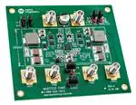
The MAX17233 evaluation kit (EV kit) is a fully assembled
and tested application circuit board for the MAX17233
high-voltage, dual synchronous step-down controller. The
EV kit is set up to provide 5V and 3.3V from an input voltage
ranging from 6V to 36V. Each buck rail can deliver up to
5A load current. The EV kit’s switching frequency is set
at 2.2MHz for both buck converters. Various jumpers are
provided to help evaluate features of the MAX17233 IC.
Features
●● Dual, Synchronous Step-Down Controllers Operate at
180° Out-of-Phase to Reduce Switching Noise
●● 6V to 36V Wide Input Supply Range
●● Buck Output Voltage: 5V and 3.3V Fixed/Adjustable
Between 1V and 10V
●● Current-Mode Controllers with Forced-PWM and
Skip Modes
●● Resistor-Configurable Frequency Between 1MHz
and 2.2MHz
●● 89% Peak Efficiency @ 6V Input in Skip-Mode
●● FSYNC Input and Power-Good Output
●● Proven 4-Layer 2oz Copper PCB Layout
●● Demonstrates 2800mil x 1300mil Solution Size
●● Fully Assembled and Tested
EV Kit Contents
●● MAX17233 EV Kit Board
Quick Start
Recommended Equipment
●●
●●
●●
●●
MAX17233 EV kit
6V to 36V, 15A power supply
Two voltmeters
Two electronic loads capable of sinking 5A each
Procedure
The EV kit is fully assembled and tested. Follow the steps
below to activate the board. Caution: Do not turn on the
power supply until all connections are completed.
1) Verify that all jumpers are in their default configurations
according to Table 1.
2) Connect the positive and negative terminals of the
power supply to the VBAT and PGND banana jacks,
respectively.
3) Connect the positive terminal of the first electronic
load to the VOUT1 banana jack. Connect the ground
terminal of the electronic load to the corresponding
PGND banana jack.
4) Connect the positive terminal of the second electronic
load to the VOUT2 banana jack. Connect the ground
terminal of the electronic load to the corresponding
PGND banana jack.
5) Set the power-supply voltage to 14V.
6) Turn on the power supply.
7) Enable the electronic loads.
8) Verify that VOUT1 is approximately 5V.
9) Verify that VOUT2 is approximately 3.3V.
Ordering Information appears at end of data sheet.
19-8451; Rev 0; 2/16
�Evaluates: MAX17233, MAX17232
MAX17233 Evaluation Kit
Table 1. Default Jumper Settings
JUMPER
DEFAULT SHUNT POSITION
JU1, JU2
1-2
Buck outputs enabled.
JU6
1-2
Forced-PWM mode.
JU7
1-2
Switches to EXTVCC. Internal regulator disabled.
JU8, JU9
Installed
Detailed Description of Hardware
The MAX17233 EV kit, which evaluates the MAX17233
high-voltage, dual synchronous step-down controller, can
supply up to two rails. The EV kit includes two current-mode
buck outputs that are fixed to 5V and 3.3V, or configurable
from 1V to 10V with external resistor-dividers. The current
capability is 5A per rail. Both outputs are current limited and
can be controlled independently through their respective
enable inputs EN_.
Switching Frequency/External Synchronization
The EV kit switching frequency can be adjusted from
1MHz to 2.2MHz by changing the FOSC resistor R136.
The EV kit can also be synchronized to an external clock
by connecting the external clock signal to the FSYNC
test point and AGND. Refer to the Switching Frequency/
External Synchronization section of the MAX17233 IC
data sheet for more details.
Enable Control
The EV kit features jumper JU1 to independently control
the enable input of VOUT1 and jumper JU2 to control the
enable input of VOUT2. Connect the EN_ pin to VBAT
(pins 1-2) to enable VOUT_. Connect the EN_ pin to
PGND (pins 2-3) to disable VOUT_. See Table 2.
Mode of Operation
The EV kit features jumper JU6 to configure the mode
switch-control input (Table 3). Drive FSYNC high (pins 1-2
of JU6) to enable forced-PWM mode. Drive FSYNC low
(pins 2-3 of JU6) to enable skip mode under light loads.
EXTVCC Switchover Comparator
The internal linear regulator can be bypassed by connecting
an external supply (3.1V to 5.2V) or the output of one of
the buck converters to EXTVCC. BIAS internally switches
to EXTVCC and the internal linear regulator turns off.
If VEXTVCC drops below VTH,EXTVCC = 3.1V(min), the
internal regulator enables and switches back to BIAS.
See Table 4.
www.maximintegrated.com
FUNCTION
PGOOD_ pulls up to BIAS when OUT_ is in regulation.
Table 2. Enable Control (JU1, JU2)
SHUNT
POSITION
EN_ PIN
VOUT_
1-2*
Connected to VBAT
Enabled
2-3
Connected to PGND
Disabled
*Default configuration.
Table 3. Mode of Operation (JU6)
SHUNT
POSITION
FSYNC
PIN
MODE
1-2*
Connected to BIAS
Forced-PWM mode
2-3
Connected to AGND
Skip mode
*Default configuration.
Table 4. EXTVCC (JU7)
SHUNT
POSITION
EXTVCC
PIN
1-2
Connected to
VOUT1
Switches to EXTVCC.
Internal regulator
disabled.
1-3*
Connected to
PGND
Internal regulator
enabled.
1-4
Connected to
VOUT2
Switches to EXTVCC.
Internal regulator
disabled.
BIAS
*Default configuration.
Buck Output Monitoring (PGOOD_)
The EV kit provides two power-good output test points
(PGOOD1 and PGOOD2) to monitor the status of the two
buck outputs (OUT1 and OUT2). Each PGOOD_ goes
high (high impedance) when the corresponding regulator
output voltage is in regulation. Each PGOOD_ goes low
when the corresponding regulator output voltage drops
below 15% (typ) or rises above 10% (typ) of its nominal
regulated voltage. PGOOD_ asserts low during soft-start
Maxim Integrated │ 2
�MAX17233 Evaluation Kit
and in shutdown. PGOOD_ becomes high impedance
when OUT_ is in regulation. To obtain a logic signal, pull
up PGOOD_ to BIAS by installing shunts on JU8 and JU9.
Setting the Output Voltage in Buck Converters
To externally adjust the output voltage OUT1 between 1V
and 10V, remove R122. Connect a resistive divider from the
output OUT1 to FB1 to AGND. Place appropriate resistors in
positions R119 and R120 according to the following equation:
V
=
R119 R120 OUT1 − 1
VFB1
where VFB1 = 1V (typ).
To externally adjust the output voltage OUT2 between
1V and 10V, remove R134. Connect a resistive divider
from the output OUT2 to FB2 to AGND. Place appropriate
resistors in positions R131 and R132 according to the
following equation:
Evaluates: MAX17233, MAX17232
Evaluating the MAX17232 on the
MAX17233 EV Kit
The MAX17233 EV kit can be modified to operate the
MAX17232. The MAX17232 operates at a switching
frequency of 400kHz, which requires a change in the
following components:
1) Replace U1 with the MAX17232 IC.
2) Replace R136 (RFOSC) with 80.6kΩ to achieve 400kHz
switching frequency.
3) Replace the buck inductors (L7, L8) with a 6.8µH 7A
inductor.
Contact Technical Support at www.maximintegrated.
com/support for any further questions.
V
=
R131 R132 OUT2 − 1
VFB2
where VFB2 = 1V (typ).
www.maximintegrated.com
Maxim Integrated │ 3
�MAX17233 Evaluation Kit
Evaluates: MAX17233, MAX17232
Component Suppliers
SUPPLIER
WEBSITE
NXP
www.nxp.com
Fairchild Semiconductor
www.fairchildsemi.com
IRC, Inc.
www.irctt.com
Murata Electronics North America, Inc.
www.murata.com
Panasonic Corp.
www.panasonic.com
TDK Corp.
www.component.tdk.com
Vishay
www.vishay.com
Note: Indicate that you are using the MAX17233 when contacting these component suppliers.
Component Information, PCB Layout,
and Schematic
See the following links for component information, PCB
layout diagrams, and schematic.
●● MAX17233 EV BOM
Ordering Information
PART
TYPE
MAX17233EVKIT#
EV Kit
#Denotes RoHS compliant.
●● MAX17233 EV PCB Layout
●● MAX17233 EV Schematic
●● MAX17233 EV Minimal Component Schematic
www.maximintegrated.com
Maxim Integrated │ 4
�MAX17233 Evaluation Kit
Evaluates: MAX17233, MAX17232
Revision History
REVISION
NUMBER
REVISION
DATE
0
2/16
DESCRIPTION
Initial release
PAGES
CHANGED
—
For pricing, delivery, and ordering information, please contact Maxim Direct at 1-888-629-4642, or visit Maxim Integrated’s website at www.maximintegrated.com.
Maxim Integrated cannot assume responsibility for use of any circuitry other than circuitry entirely embodied in a Maxim Integrated product. No circuit patent licenses
are implied. Maxim Integrated reserves the right to change the circuitry and specifications without notice at any time.
Maxim Integrated and the Maxim Integrated logo are trademarks of Maxim Integrated Products, Inc.
© 2016 Maxim Integrated Products, Inc. │ 5
�MAX17233EVKIT#: Rev A
Item Component Description
0001
0002
0003
0004
0005
0006
0007
0008
0009
0010
0011
0012
0013
0014
0015
0016
0017
0018
0019
0020
0021
0022
0023
0024
0025
0026
0027
0028
0029
63MIL DRILL SIZE test point (BLK)
63MIL DRILL SIZE test points (RED)
0.1uF±10%, 50V X7R ceramic capacitors (0603)
47uF ±20%, 16V X7R ceramic capacitors (2220)
4700pF ±10% 50V X7R ceramic capacitors (0402)
22pF ±5% 50V C0G ceramic capacitor (0402)
6.8uF ±10%, 16V X7R ceramic capacitor (1206)
2.2uF ±10%, 10V X7R ceramic capacitor (0603)
33pF ±5% 50V C0G ceramic capacitor (0402)
47uF, 50V ±20% aluminum electrolytic capacitor (8.0x6.2mm)
4.7uF±10%, 50V X7R ceramic capacitors (1210)
200mA, 30V Schottky diodes (SOT23)
5A, 40V Schottky Diodes (SOD-128)
3-pin headers (CUT TO FIT)
4-pin header (CUT TO FIT)
2-pin headers (CUT TO FIT)
2.2uH 12A power inductors
40V, 7.6A N-channel MOSFETs (8-SOIC)
JACKs, BANNANA, UNINSULATED, PANEL MOUNT
1kΩ 5% resistors (0603)
0Ω 5% resistors (0603)
0.012Ω, ±1%, 1W sense resistors (2010)
22.1kΩ 1% resistor (0603)
1Ω ±5%, resistor (0603)
14kΩ 1% resistor (0603)
13.7kΩ 1% resistor (0603)
100kΩ 1% resistor (0603)
51.1kΩ % resistors (0603)
Dual Buck (28-pinTQFN 5x5x0.8mm)
Not Installed Capacitors (0603)
Not Installed Capacitors (2220)
Not Installed Resistors (0603)
0030 Shunts
0031 PC board: MAX17233 EV KIT
Qty
1
3
5
4
2
1
1
1
1
1
6
2
2
3
1
2
2
4
6
2
8
2
1
1
1
1
1
2
1
0
0
0
6
1
Reference Designators
Manufacturer
Part Number
AGND
FSYNC, PGOOD1 TEST, PGOOD2 TEST
C1, C2, C3, C75, C83
C76, C77, C84, C85
C78, C86
C79
C81
C82
C87
C88
C90-C93, C97, C116
D20, D21
D22, D23
JU1, JU2, JU6
JU7
JU8, JU9
L7, L8
Q13-Q16
PGND (3x), VBAT, VOUT1, VOUT2
R1, R2
R113-R115, R122, R125-R127, R134
R116, R128
R123
R124
R135
R136
R137
R156, R157
U1
C4, C5, C102, C103
C117, C118
R119, R120, R131, R132
See Jumper Table
2 oz Cu
Keystone Electronics
Keystone Electronics
Murata
TDK
Murata
Murata
TDK
Murata
Murata
Panasonic
Murata
Fairchild
NXP
SULLINS
SULLINS
SULLINS
Vishay
Fairchild
JOHNSON
Any
Any
IRC
Any
Any
Any
Any
Any
Any
Maxim
5011
5010
GRM188R71H104K
CGA9N3X7R1C476M
GRM155R71H472K
GRM1555C1H220J
C3216X7R1C685K
GRM188R71A225K
GRM1555C1H330J
EEEFK1H470P
GCM32ER71H475KA55L
BAT54
PMEG4050EP
PEC36SAAN
PEC36SAAN
PEC36SAAN
IHLP4040DZER2R2M01
FDMC8015L
108-0740-001
Any
Any
LRF2010LF-01-R012-F
Any
Any
Any
Any
Any
Any
MAX17233ETIR+
Kycon
Network PCB
SX1100-B
MAX17233 EV KIT
�X3
PGND
PGND
JU7
JU6 JU6
1
2
3
JU7
FSYNC FSYNC
3
1.0"
1 of 6
Q16
D23
D23x2
C84R128
C85
2 1 4
EXTVCC
J6 J5
X7
PGND
C3x1
C3x2
Q15x10
C92x1 C93x1
C92x2 C93x2
Q15x5
Q15x6
Q15x7
Q15x8
Q15x9
L8
L8x1
L8x2
C5
C88x1
R1 R1
R2 R2
PGOOD1_TEST PGOOD2_TEST
R1x1
R1x2
R156
R156x2 R156x1
R156 JU8 2 JU9 R157
PGOOD1_TEST PGOOD2_TEST
PGO D1_TESTx1 JU8x2 JU8x1
1
R2x2
R2x1
R157
R157x2 R157x1
PGO D2_TESTx1 JU9x2 JU9x1
X2x1
PGND
X6x21
J4x1
C88x2
JU8
R128x1 R128x2
C85x1 C84x1
Q15x4
C5x1 C5x2
C3
C85x2 C84x2
Q15x3
Q15x2
Q16x6
Q16x5
Q16x7
Q15x1
R127
R115 C4
X6
R128
Q16x10
Q16x9
D23x1
Q16x4
Q16x3
Q16x2
Q16x8
C83x2
C83x1
D21x2
D21x3
D21x1
C4x1 C4x2
C93
C92
J5x1
R125x2
1
Q16x1
R126x2
R126x1
R127x1 R127x2
Q15
VOUT2x21
R125
D23
R131x2
R131x1
R125x1
U1
J6x1
R132R131
R132
R131
R132x2
R132x1
C75x1
R115x1 R115x2
R113x1
1
R134
C86x2
C86x1
C87x1
U1x22
U1x23
U1x24
U1x25
U1x26
U1x27
U1x28
VBATx21
J3x1
VBAT
X7x21
C87C86
C87x2
U1x32
U1x 5 U1x 6 U1x 7 U1x 8 U1x 9 U1x20 U1x21
U1x33
U1x29
U1x31
D20x2
D20x3
D20x1
+
D21
C83
R126
R134x1 R134x2
R135x2
R135x1
U1x14
U1x13
U1x12
U1x30
C75x2
R113x2
Q13x6
Q13x5
C88
R136
R137x1
C2
R137x2
C2
R136x1 R136x2
U1x11
U1x10
U1x7 U1x6 U1x5 U1x4 U1x3 U1x2 U1x1
U1
U1x9
Q13x10
D20
C75
R113
C2x1
R114x1
Q13x4
Q13x3
Q13x7
J3 C88J4
VBAT
C97x1 C116x1
U1x8
R120x1
R120x2
Q14x6
Q14x5
Q14x4
Q13x2
Q13x1
Q14x9 Q13x9
Q14x3
R114x2
Q14x7
Q14x2
Q14x1
C4 D21C5 Q15
Q13 D20
C75
R127C83
R126
R113R115
Q14 R114
R125 Q16
1
JU6x3
C79x2
C79x1
R114
JU6x2
C82x1 C82x2
C82
C97x2 C116x2 C2x2
R124x1
R123x1
Q14x10
Q13x8
C90x2 C91x2
C90x1 C91x1
Q13
FSYNCx1
R136 R135 R134 R132 R131
R137
C87 C86
R135
C82 C116 C116 R137
C84
AGND C97 C97
C85
C81x2
R119R120
R119x1
R119x2
Q14
R124x2
R122
C78x2
1
C78x1
1
R123x2
R122x1 R122x2
Q14x8
C1x2
C1x1
DATE: JAN 2016
MAX17233 EVKIT
REV-A
X14
1-888-629-4642
01/16 AMD X5
www.maximintegrated.com
X5x1
VOUT1
C1
X14x1
VOUT1
C91
C90
JU6x1
C76
R119 R120
C78 C79
C78 C79
R123
R123
C81
C81
C77
R124
C76
R124
AGND
C81x1
D22x1
JU2x3 JU2x2
X1
JU7x2
JU7x1 JU7x3
JU7x4
R116C77
D22
C91
C90
L7 C1
D22x2
JU2x1
2
3
C76x2 C77x2
L7x2
L7 D22
C76x1 C77x1
JU2
EN2
AGNDx1
1300mil
JU1x1
JU1 JU2
JU1x3 JU1x2
LAYER
R122
L7x1
DIS
R116x2 R116x1
EN
1
J2x1
R116
JU1
EN1
PGNDx21
J1x1
J1 J2
VOUT1x21
X4x1
X4
X14x2
X3x1
MAX17233 EVKIT
REV
A
TOP SILKSCREEN
ALL UNITS ARE IN 0.001"
JU9
X2
C93
C92
C3 L8
2800mil
VOUT2
VOUT2
�X3
JU6
JU6x3
JU6x2
FSYNC
JU7
1.0"
2 of 6
U1x32
R131x2
R131x1
R132x2
R132x1
U1x 5 U1x 6 U1x 7 U1x 8 U1x 9 U1x20 U1x21
U1x33
U1x31
U1x29
U1x30
D23x2
R132R131
U1x28
U1x27
U1x26
Q16x4
Q16x3
Q16x2
Q16x1
R125x2
R125x1
U1x22
U1x23
U1x24
U1x25
Q15x3
Q15x4
Q15x2
Q16x6
Q16x5
Q16x7
Q15x1
D21x2
D21x1
C3x1
C3x2
Q15x10
Q15x5
Q15x6
Q15x7
Q15x8
Q15x9
C5x1 C5x2
D21x3
C4x1 C4x2
D20x2
D20x3
D20x1
C92x1 C93x1
C92x2 C93x2
J6 J5
X7
L8x1
C88x2
X6x21
X6
R1x1
R1x2
R156x2 R156x1
J4x1
C88x1
R156 JU8
C84R128
C85
R128x1 R128x2
L8
L8x2
VBATx21
J3x1
R1
C85x1 C84x1
D23x1
D23
C85x2 C84x2
C83x2
R126x2
Q16x8
C83x1
R126x1
R127x1 R127x2
Q16x9
Q16x10
C75x1
R113x1
R115x1 R115x2
C75x2
R113x2
Q13x6
Q13x5
Q13x4
Q13x10
Q13x3
Q14x6
Q14x5
C93
C92
C3
J5x1
U1x7 U1x6 U1x5 U1x4 U1x3 U1x2 U1x1
Q14x10
Q14x9 Q13x9
Q13x2
Q13x8
Q13x7
Q13x1
Q14x8
Q14x7
J3 C88J4
VOUT2x21
C86x2
C86x1
C87x1
C87x2
R134x1 R134x2
R135x2
R135x1
U1x14
U1x13
U1x12
U1x11
U1x10
U1x9
U1x8
R120x1
C87C86
J6x1
R137x1
R136x1 R136x2
C2x1
C79x2
R114x1
R114x2
Q14x4
Q14x3
Q14x2
U1
R137x2
C97x1 C116x1
C2x2
R120x2
R119x1
C4 D21C5 Q15
Q13 D20
C75
R127C83
R126
R113R115
Q14 R114
R125 Q16
Q14x1
VBAT
X7x21
C82x1 C82x2
C79x1
R119x2
R119R120
C97x2 C116x2
R124x1
R123x1
C78x2
C78 C79
C78x1
C90x2 C91x2
C90x1 C91x1
JU2x1
JU1x1
PGOOD1_TEST PGOOD2_TEST R2
X14
R2x2
R2x1
JU9 R157
R157x2 R157x1
PGO D2_TESTx1 JU9x2 JU9x1
PGO D1_TESTx1 JU8x2 JU8x1
X2x1
DATE: JAN 2016
X5
X5x1
PGND
C81x2
R135 R134
R122 R123 C2R136R137
C81 C116
C82
AGND R124 C97
R123x2
R122x1 R122x2
C1x2
C1x1
C1
R124x2
C81x1
D22x1
C91
C90
FSYNCx1
C76
AGNDx1
D22x2
JU2x3 JU2x2
JU1x3 JU1x2
JU1 JU2
JU7x2
JU7x1 JU7x3
JU7x4
R116C77
C76x2 C77x2
L7x2
L7x1
L7 D22
C76x1 C77x1
R116x2 R116x1
X4
JU6x1
J2x1
VOUT1
PGNDx21
J1x1
J1 J2
VOUT1x21
X4x1
LAYER
X14x1
X14x2
X3x1
MAX17233 EVKIT
REV
A
COMPONENT SIDE
ALL UNITS ARE IN 0.001"
X2
VOUT2
�X3
JU6
JU6x3
JU6x2
JU6x1
FSYNC
JU7
1.0"
3 of 6
J6x1
J6 J5
X7
J5x1
U1x32
PGOOD1_TEST PGOOD2_TEST
JU8 JU9
PGO D2_TESTx1 JU9x2 JU9x1
PGO D1_TESTx1 JU8x2 JU8x1
X6x21
J4x1
J3 J4
VOUT2x21
X7x21
U1x31
U1x33
U1
U1x30
U1x29
VBATx21
VBAT
J3x1
JU2x1
JU2x3 JU2x2
X2x1
DATE: JAN 2016
X14
X5
X5x1
PGND
JU7x2
JU7x1 JU7x3
JU7x4
AGNDx1
JU1x1
JU1 JU2
JU1x3 JU1x2
X4
FSYNCx1
J2x1
VOUT1
PGNDx21
J1x1
J1 J2
VOUT1x21
X4x1
LAYER
X14x1
X14x2
X3x1
MAX17233 EVKIT
REV
A
LAYER 2 GND
ALL UNITS ARE IN 0.001"
X6
X2
AGND
VOUT2
�X3
JU6
JU6x3
JU6x2
JU6x1
FSYNC
JU7
1.0"
4 of 6
J6x1
J6 J5
X7
J5x1
U1x32
PGOOD1_TEST PGOOD2_TEST
JU8 JU9
PGO D2_TESTx1 JU9x2 JU9x1
PGO D1_TESTx1 JU8x2 JU8x1
X6x21
J4x1
J3 J4
VOUT2x21
X7x21
U1x31
U1x33
U1
U1x30
U1x29
VBATx21
VBAT
J3x1
JU2x1
JU2x3 JU2x2
X2x1
DATE: JAN 2016
X14
X5
X5x1
PGND
JU7x2
JU7x1 JU7x3
JU7x4
AGNDx1
JU1x1
JU1 JU2
JU1x3 JU1x2
X4
FSYNCx1
J2x1
VOUT1
PGNDx21
J1x1
J1 J2
VOUT1x21
X4x1
LAYER
X14x1
X14x2
X3x1
MAX17233 EVKIT
REV
A
LAYER 3 PWR
ALL UNITS ARE IN 0.001"
X6
X2
AGND
VOUT2
�X3
JU6
JU6x3
JU6x2
FSYNC
JU7
1.0"
5 of 6
J6 J5
X7
J5x1
VOUT2x21
AGND
PGOOD1_TEST PGOOD2_TEST
JU8 JU9
PGO D2_TESTx1 JU9x2 JU9x1
PGO D1_TESTx1 JU8x2 JU8x1
X6x21
J4x1
J3 J4
C118
C118x1
C118x2
U1x32
U1x33
C102
C102x2
C102x1
U1x31
U1x30
U1
J6x1
U1x29
J3x1
VBATx21
VBAT
X7x21
C103x1
C103x2
JU2x1
JU2x3 JU2x2
X2x1
DATE: JAN 2016
X14
X5
X5x1
PGND
JU6x1
AGNDx1
C103
JU7x2
JU7x1 JU7x3
JU7x4
C117
C117x2
C117x1
JU1x1
JU1 JU2
JU1x3 JU1x2
X4
FSYNCx1
J2x1
VOUT1
PGNDx21
J1x1
J1 J2
VOUT1x21
X4x1
LAYER
X14x1
X14x2
X3x1
MAX17233 EVKIT
REV
A
SOLDER SIDE
ALL UNITS ARE IN 0.001"
X6
X2
VOUT2
�X3
JU6
JU6x3
JU6x2
FSYNC
JU7
1.0"
6 of 6
J6x1
J6 J5
X7
J5x1
AGND
PGOOD1_TEST PGOOD2_TEST
JU8 JU9
PGO D2_TESTx1 JU9x2 JU9x1
PGO D1_TESTx1 JU8x2 JU8x1
X6x21
J4x1
J3 J4
C118
C118x1
C118x2
711C
VOUT2x21
X7x21
U1x32
C102
C102x2
C102x1
U1x31
U1x33
U1
U1x30
U1x29
VBATx21
VBAT
J3x1
JU2x1
JU2x3 JU2x2
X2x1
DATE: JAN 2016
X14
X5
X5x1
PGND
C103x1
C103x2
301C
JU6x1
AGNDx1
C103
JU7x2
JU7x1 JU7x3
JU7x4
C117
C117x2
C117x1
JU1x1
JU1 JU2
JU1x3 JU1x2
X4
FSYNCx1
J2x1
VOUT1
PGNDx21
J1x1
J1 J2
VOUT1x21
X4x1
LAYER
X14x1
X14x2
X3x1
MAX17233 EVKIT
REV
A
BOTTOM SILKSCREEN
ALL UNITS ARE IN 0.001"
X6
X2
201C
811C
VOUT2
�6
5
4
3
2
1
REVISION RECORD
LTR
D
VBAT
1
C75
0.1uF
50V
3
D
VBAT
7
8
1
C76
47uF
16V
PGND
BIAS
R113
R126
0
0
C5
OPEN
VBAT
6
7
C93
4.7uF
50V
8
5
4
C92
4.7uF
50V
C3
0.1uF
50V
J5
VOUT2
1
Q15
1
LX2
3
VOUT2
6
8
L8
2.2uH
0.012
1%
VOUT2
3.3V, 5A
22
8
DL2
R125
21
4
5
Q16
1
0
3
C85
47uF
16V
D23
LX1
7
5
1
6
LX2
23
DH2
24
BST2
25
26
EN2
LX1
EN1
27
4
1
R128
C84
47uF
16V
C118
OPEN
2
7
PGND
2
D22
C77
47uF
16V
0
1
2.2uH
R114
4
Q14
2
C
C117
OPEN
D21
3
L7
1
0.012
1%
C83
0.1uF
50V
2
2
R116
3
5
3
VOUT1
3
JU2
6
Q13
VOUT1
5V, 5A
2
BST1
C90
4.7uF
50V
2
0
28
1
C91
4.7uF
50V
1
R127
DH1
C1
0.1uF
50V
1
R115
C4
OPEN
J1
VOUT1
DATE:
LX2
JU1
BIAS
APPROVED:
VBAT
LX1
D20
ECO NO:
3
1
2
DL1
PGND2
C
20
J6
PGND
0
2
1
3
PGND1
CS2
J2
PGND
19
U1
1
4
C103
OPEN
5
R119
OPEN
6
MAX17233ETIR+
CS1
OUT2
OUT1
FB2
FB1
COMP2
18
R131
OPEN
17
14k
1%
C86
4700pF
R134
BIAS
0
EP
15
14
FSYNC
PGOOD2
13
PGOOD1
12
11
IN
EXTVCC
10
C79
22pF
AGND
22.1k
1%
FOSC
BIAS
C78
4700pF
COMP1
8
R122
0
7
9
R123
R132
OPEN
R135
16
C87
33pF
R120
OPEN
C102
OPEN
R136
13.7k
1%
BIAS
B
C81
6.8uF
B
R137
AGND
100k
1%
VOUT1
BIAS
JU7
3
2
FSYNC
R124
1
1
1
4
C82
2.2uF
JU6
2
3
GND
VOUT2
PGND
J3
VBAT
1
PGOOD2_TEST
VBAT
VBAT
PGND
J4
PGND
R2
C2
0.1uF
50V
+
C88
47uF
50V
C116
4.7uF
50V
C97
4.7uF
50V
1k
R157
PGOOD1_TEST
2 JU9 1
51.1k
R1
R156
1k
51.1k
2 JU8 1
BIAS
1
A
A
TITLE:
MAX17233 EVKIT
PCB PART NUMBER:
REV:
A
DRAWN:
DATED:
JAN 2016
SHEET: 1 OF 1
�6
5
4
3
2
1
REVISION RECORD
LTR
ECO NO:
APPROVED:
DATE:
D
D
LX2
LX1
C75
0.1uF
50V
VBAT
C83
0.1uF
50V
VBAT
D21
D20
1
BIAS
3
3
VBAT
1
BIAS
6
7
8
5
4
VBAT
7
8
J2
PGND
7
C76
47uF
16V
1
0.012
1%
22
7
8
5
1
6
LX2
23
DH2
24
BST2
25
EN2
26
EN1
DL2
4
21
Q16
1
5
3
C85
47uF
16V
D23
LX1
6
8
2.2uH
J5
VOUT2
1
C84
47uF
16V
2
D22
C77
47uF
16V
1
2.2uH
4
Q14
2
C
LX1
L8
R128
2
0.012
1%
VOUT2
L7
1
R116
1
27
4
1
2
VOUT1
3
5
3
VOUT1
C3
0.1uF
50V
2
Q13
J1
C92
4.7uF
50V
Q15
1
LX2
6
BST1
C90
4.7uF
50V
28
C91
4.7uF
50V
DH1
C1
0.1uF
50V
C93
4.7uF
50V
3
2
DL1
PGND2
J6
PGND
1
C
20
1
2
3
PGND1
CS2
19
U1
4
MAX17233ETIR+
CS1
5
OUT2
OUT1
6
FB2
FB1
COMP2
18
17
BIAS
R135
16
C87
33pF
FSYNC
15
14
PGOOD2
13
PGOOD1
12
IN
10
11
BIAS
EXTVCC
FOSC
AGND
COMP1
C79
22pF
C86
4700pF
EP
7
22.1k
1%
8
C78
4700pF
9
R123
14k
1%
R136
13.7k
1%
BIAS
B
B
C81
6.8uF
BIAS
R124
VOUT1
1
C82
2.2uF
GND
PGND
VBAT
J3
VBAT
1
J4
PGND
1
A
C2
0.1uF
50V
+
C88
47uF
50V
C116
4.7uF
50V
C97
4.7uF
50V
A
TITLE:
MAX17233_MINIMAL_COMPONENT_CIRCUIT
PCB PART NUMBER:
REV:
A
DRAWN:
DATED:
A. DIMAPILIS
NOV 2015
SHEET:
OF
1 1
�