EVALUATION KIT AVAILABLE
Click here for production status of specific part numbers.
MAX17250
2.7V to 18V Input, Boost Converter with 0.1μA
True Shutdown, Short-Circuit Protection
and Selectable Input Current Limit
General Description
Benefits and Features
The MAX17250 DC-DC boost converter is a high-efficiency,
low quiescent current, synchronous boost (step-up)
converter with True Shutdown™, program
mable input
current limit, and short-circuit protection. The MAX17250
has a wide input voltage range of 2.7V to 18V and
generates an output voltage of 3V to 18V. The MAX17250
has a maximum on-time of 800ns and implements three
modes of operation. The first mode of operation is a
soft-start mode at power-up. The second mode of
operation is normal operation and utilizes a fixed on-time/
minimum off-time Pulse Frequency Modulation (PFM)
architecture that uses only 60μA (typ) quiescent
current due to the converter switching only when needed.
The last mode is True Shutdown, where the output is
completely disconnected from the input, and the battery
drain is minimized to 0.1μA (typ) shutdown current. The
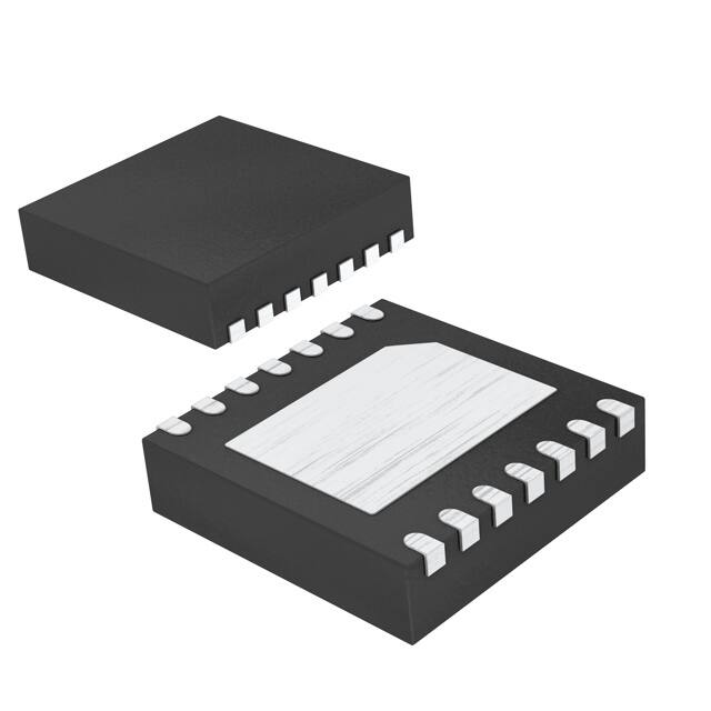
MAX17250 is available in a compact, 12-bump, 1.72mm
x 1.49mm WLP or a 14-pin, 3mm x 3mm TDFN package.
●● Input Voltage Range 2.7V to 18V
• 1 or 2 Cell Li-ion Batteries
●● Output Voltage Range 3V to 18V, > VIN
●● Integrated Power FETs
●● Selectable Input Peak Current Limit (ISET)
• 3.5A, 2.7A, or 1.85A
●● 93% Efficiency
●● Low Power
• 0.1μA True Shutdown Current
• 60μA Quiescent Current
●● Protection
• True Shutdown Prevents Current Flowing Between
Input and Output
• Soft-Start Inrush Protection
• Short-Circuit Protection
• Overtemperature Protection
• -40°C to +125°C Operation
Applications
●●
●●
●●
●●
●●
Digital Cameras
Battery Powered Internet of Things (IoT) Device
1 or 2 Cell Li-ion Battery Applications
Display Supply
Buzzer/Alarm Driver
Ordering Information appears at end of data sheet.
True Shutdown is a trademark of Maxim Integrated Products.
Typical Application Circuit
L
3.0V to 8.4V
IN
2.2µH
0.1µF
LX
IN
CIN
2x10µF
GND
EN
MAX17250
EN
VL
ISET
AGND
19-100359; Rev 2; 10/19
BST
OUT
PVH
PGND
4.7nF
FB
VL
12V
OUT
CPVH
2x22µF
Rz
1kΩ
R1
84.5kΩ
2.2µF
R2
10kΩ
COUT
10µF
�MAX17250
2.7V to 18V Input, Boost Converter with 0.1μA
True Shutdown, Short-Circuit Protection
and Selectable Input Current Limit
Absolute Maximum Ratings
IN, LX, OUT, PVH to AGND...................................-0.3V to +22V
BST to LX.................................................................-0.3V to +6V
EN, ISET, FB, VL to AGND......................................-0.3V to +6V
PGND to AGND.....................................................-0.3V to +0.3V
WLP LX RMS Current.............................-3.2ARMS to +3.2ARMS
TDFN LX RMS Current.......................-2.58ARMS to +2.58ARMS
Short-Circuit Between OUT and GND........................Continuous
WLP Continuous Power Dissipation
(TA = +70°C, derate 13.7mW/°C above +70°C.)........1096mW
TDFN Continuous Power Dissipation
(TA = +70°C, derate 24.4mW/°C above +70°C.).....1951.2mW
Operating Temperature Range.......................... -40°C to +125°C
Junction Temperature.......................................................+150°C
Storage Temperature Range............................. -65°C to +150°C
Lead Temperature (soldering, 10 seconds)......................+300°C
Soldering Temperature (reflow)........................................+260°C
Stresses beyond those listed under “Absolute Maximum Ratings” may cause permanent damage to the device. These are stress ratings only, and functional operation of the device at these
or any other conditions beyond those indicated in the operational sections of the specifications is not implied. Exposure to absolute maximum rating conditions for extended periods may affect
device reliability.
Package Information
14-TDFN
Package Code
T1433+2C
Outline Number
21-0137
Land Pattern Number
90-0063
Thermal Resistance, Single-Layer Board:
Junction to Ambient (θJA)
54°C/W
Junction to Case (θJC)
8°C/W
Thermal Resistance, Four-Layer Board:
Junction to Ambient (θJA)
41°C/W
Junction to Case (θJC)
8°C/W
12-WLP
Package Code
N121B1+1
Outline Number
21-100158
Land Pattern Number
Refer to Application Note 1891
Thermal Resistance, Four-Layer Board:
Junction to Ambient (θJA)
72.82°C/W
Junction to Case (θJC)
N/A
For the latest package outline information and land patterns (footprints), go to www.maximintegrated.com/packages. Note that a “+”,
“#”, or “-” in the package code indicates RoHS status only. Package drawings may show a different suffix character, but the drawing
pertains to the package regardless of RoHS status.
Package thermal resistances were obtained using the method described in JEDEC specification JESD51-7, using a four-layer board.
For detailed information on package thermal considerations, refer to www.maximintegrated.com/thermal-tutorial.
www.maximintegrated.com
Maxim Integrated │ 2
�MAX17250
2.7V to 18V Input, Boost Converter with 0.1μA
True Shutdown, Short-Circuit Protection
and Selectable Input Current Limit
Electrical Characteristics
(VIN = 7.2V, VPVH = VOUT = 10V, VEN = 5V, TA = -40°C to +125°C, typical values are at TA = +25°C, unless otherwise noted.) (Note 1)
PARAMETER
SYMBOL
CONDITIONS
Input Voltage Range
VIN
Quiescent Supply
Current
IQ
Not switching, 105% TA = 25°C
of VOUT_TARGET,
TA = -40°C to 125°C
Shutdown Current
ISD
VEN = VOUT = 0V,
VPVH = 7.2V
VIN < VOUT_TARGET
FB Accuracy
ACC
VFB falling, when LX starts switching
Inductor Peak Current
Limit
IPEAK
60
MAX
UNITS
18
V
80
95
TA = 25°C
VOUT
VUVLO
TYP
2.7
Output Voltage Range
Input Undervoltage
Threshold
MIN
