EVALUATION KIT AVAILABLE
Click here for production status of specific part numbers.
MAX17270/MAX17271
nanoPower Triple-Output, Single-Inductor,
Multiple-Output (SIMO) Buck-Boost Regulator
General Description
The MAX17270/MAX17271 are 3-output switching
regulators designed for applications requiring efficient
regulation of multiple supplies in a very small space, such
as wearable electronic devices.
The parts use a buck-boost architecture that regulates
three outputs using a single, small 2.2µH inductor at
efficiencies up to 85%. This results in smaller board space
while delivering better total system efficiency than equivalent
power solutions using one buck and linear regulators.
The supply current is 0.85µA when only one output is
enabled, plus 0.2µA for each additional output enabled.
This SIMO (Single-Input Multiple-Output) regulator utilizes the entire battery voltage range due to its ability to
create output voltages that are above, below, or equal to
the input voltage. Peak inductor current for each output is
programmable to optimize the balance between efficiency,
output ripple, EMI, PCB design, and load capability.
Two versions are available. The MAX17270 has 3 enable
inputs and 3 output voltage programming inputs. The
MAX17271 includes an I2C interface with interrupt, a
push-button turn on/off, and a power-good indication.
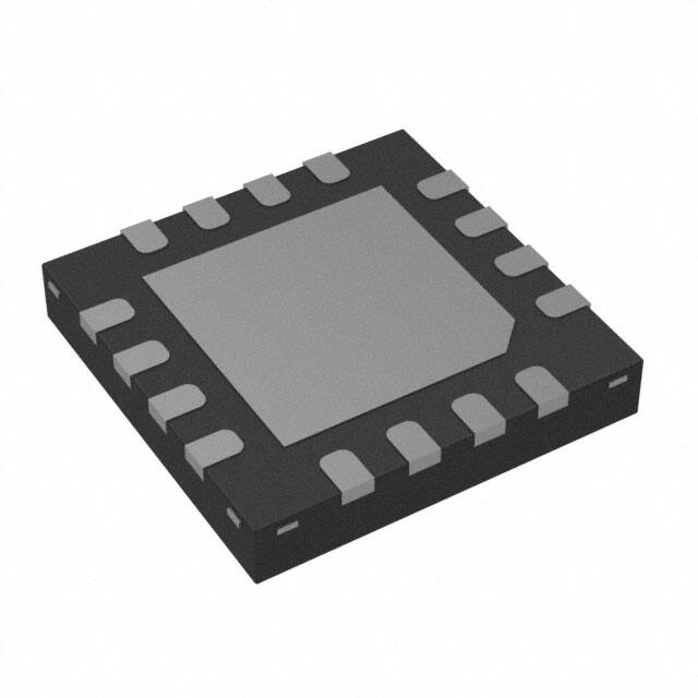
All versions are offered in either a 4 x 4, 0.4mm waferlevel package (WLP) or a 16-pin TQFN package.
Benefits and Features
●● 3-Output, Single-Inductor, Multiple-Output (SIMO)
Buck-Boost Regulator
●● 2.7V to 5.5V Input Voltage Range
●● Low-Power and Long Battery Life
• 1.3μA Operating Current (3 SIMO Channels)
• 330nA Shutdown Current
• 85% Efficiency at 3.3V Output
●● Flexible and Configurable
• I2C-Compatible Interface (MAX17271)
• Programmable Output Voltage: 0.8V to 5.175V
MAX17270/MAX17271
• Programmable Peak Current Limit
●● Robust
• Soft-Start
• Overload Protection
• Thermal Protection
●● Small Size
• 1.77mm x 1.77mm x 0.50mm, 16-Bump
0.4mm-Pitch WLP Package
• 3mm x 3mm x 0.75mm, 16-Pin TQFN Package
• Small Total Solution Size
Applications
●● Bluetooth Headsets
●● Fitness Bands
●● Watches
●● Hearables
●● Wearables
●● Internet of Things (IoT)
●● Health Monitors
19-100234; Rev 5; 9/19
Ordering Information appears at end of data sheet.
�MAX17270/MAX17271
nanoPower Triple-Output, Single-Inductor,
Multiple-Output (SIMO) Buck-Boost Regulator
Simplified Application Circuit
IN
(2.7V to 5.5V)
L
CBST
2.2µH
100nF
CIN
10µF
MAX17270/1
ENABLE INPUTS OR
I2C INTERFACE
www.maximintegrated.com
OUT3
(3.3V/50mA)
OUT2
(1.8V/75mA)
OUT1
(1.2V/80mA)
C1
22µF
C2
10µF
C3
10µF
Maxim Integrated │ 2
�MAX17270/MAX17271
nanoPower Triple-Output, Single-Inductor,
Multiple-Output (SIMO) Buck-Boost Regulator
Absolute Maximum Ratings
VPWR, OUT1, OUT2, OUT3, VIO to GND................-0.3V to +6V
Continuous Power Dissipation (WLP)
(TA = 70°C, derate 17.2mW/°C above 70°C.)............1376mW
Continuous Power Dissipation (TQFN)
(TA = 70°C, derate 20.8mW/°C above 70°C.).........1666.7mW
Operating Temperature Range............................ -40°C to +85°C
Junction Temperature.......................................................+150°C
Storage Temperature Range............................. -60°C to +150°C
Soldering Temperature (reflow)........................................+260°C
EN1, EN2, EN3, IRQB, ON, RSTB, RSEL1, RSEL2,
RSEL3 to GND.......................................-0.3V to VSUP + 0.3V
SCL, SDA to GND.......................................-0.3V to VVIO + 0.3V
VSUP to VPWR.......................................................-0.3V to +0.3V
PGND to GND.......................................................-0.3V to +0.3V
OUT1, OUT2, OUT3 Short-Circuit Duration...............Continuous
LXA Continuous Current (Note 1)..................................1.2ARMS
LXB Continuous Current (Note 2)..................................1.2ARMS
BST to LXB.................................................................-0.3V to 6V
BST to VPWR..............................................................-0.3V to 6V
Lead Temperature (soldering, 10 seconds)........................ 300°C
Note 1: LXA has internal clamping diodes to PGND and VPWR. It is normal for these diodes to briefly conduct during switching
events. Avoid steady-state conduction of these diodes.
Note 2: Do not externally bias LXB. LXB has an internal low-side clamping diode to PGND, and an internal high-side clamping
diode that dynamically shifts to the selected SIMO output. It is normal for these internal clamping diodes to briefly conduct
during switching events. When the SIMO regulator is disabled, the LXB to PGND absolute maximum voltage is -0.3V to
OUT1 + 0.3V.
Stresses beyond those listed under “Absolute Maximum Ratings” may cause permanent damage to the device. These are stress ratings only, and functional operation of the device at these
or any other conditions beyond those indicated in the operational sections of the specifications is not implied. Exposure to absolute maximum rating conditions for extended periods may affect
device reliability.
Package Information
TQFN
PACKAGE CODE
T1633+5
Outline Number
21-0136
Land Pattern Number
90-0032
THERMAL RESISTANCE, FOUR-LAYER BOARD:
Junction to Ambient (θJA)
48°C/W
Junction to Case (θJC)
10°C/W
WLP
PACKAGE CODE
N161A1+1
Outline Number
21-100190
Land Pattern Number
Refer to Application Note 1891
THERMAL RESISTANCE, FOUR-LAYER BOARD:
Junction to Ambient (θJA)
57.93
Junction to Case (θJC)
N/A
For the latest package outline information and land patterns (footprints), go to www.maximintegrated.com/packages. Note that a “+”,
“#”, or “-” in the package code indicates RoHS status only. Package drawings may show a different suffix character, but the drawing
pertains to the package regardless of RoHS status.
Package thermal resistances were obtained using the method described in JEDEC specification JESD51-7, using a four-layer board.
For detailed information on package thermal considerations, refer to www.maximintegrated.com/thermal-tutorial.
www.maximintegrated.com
Maxim Integrated │ 3
�MAX17270/MAX17271
nanoPower Triple-Output, Single-Inductor,
Multiple-Output (SIMO) Buck-Boost Regulator
Package Information (continued)
(NE - 1) X e
E
MARKING
E/2
D2/2
(ND - 1) X e
D/2
AAAA
e
C
L
D
D2
k
C
L
b
0.10 M C A B
E2/2
L
E2
0.10 C
C
L
0.08 C
C
L
A
A2
A1
L
L
e
e
maxim
integrated
TM
PACKAGE OUTLINE,
8, 12, 16L THIN QFN, 3x3x0.75mm
21-0136
www.maximintegrated.com
V
1
3
Maxim Integrated │ 4
�MAX17270/MAX17271
nanoPower Triple-Output, Single-Inductor,
Multiple-Output (SIMO) Buck-Boost Regulator
Package Information (continued)
Pin 1
Indicator
1
E
see Note 7
Marking
COMMON DIMENSIONS
A
A1
A
AAAA
A2
D
A3
b
D
SIDE VIEW
TOP VIEW
E
A1
A
S
A2
1.768
1.768
0.025
0.025
1.20 BASIC
1.20 BASIC
e
0.40 BASIC
SD
0.20 BASIC
0.20 BASIC
DEPOPULATED BUMPS:
NONE
SE
0.05 S
FRONT VIEW
0.28 REF
0.040 BASIC
0.27 0.03
E1
D1
A3
0.50 MAX
0.19 0.03
E1
SE
e
B
D
C
NOTES:
1. Terminal pitch is defined by terminal center to center value.
2. Outer dimension is defined by center lines between scribe lines.
3. All dimensions in millimeter.
4. Marking shown is for package orientation reference only.
5. Tolerance is ± 0.02 unless specified otherwise.
6. All dimensions apply to PbFree (+) package codes only.
7. Front - side finish can be either Black or Clear.
SD
D1
B
A
1 2 3 4
A
BOTTOM VIEW
- DRAWING NOT TO SCALE -
www.maximintegrated.com
b
0.05 M
maxim
integrated
S AB
TITLE
TM
PACKAGE OUTLINE 16 BUMPS
THIN WLP PKG. 0.4 mm PITCH,N161A1+1
APPROVAL
DOCUMENT CONTROL NO.
21-100190
REV.
B
1
1
Maxim Integrated │ 5
�MAX17270/MAX17271
nanoPower Triple-Output, Single-Inductor,
Multiple-Output (SIMO) Buck-Boost Regulator
Electrical Characteristics (continued)
(VSUP = VPWR = 3.7V, TJ = -40°C to 85°C, Typical Application Circuits, typical values are at TJ = 25°C unless otherwise specified. Limits
over the specified operating temperature and supply voltage range are guaranteed by design and characterization, and production
tested at room temperature only. )
PARAMETER
LX Peak Current Limit
(MAX17271 Only)
SYMBOL
ILIM
CONDITIONS
At LXB, TA = +25°C
MIN
TYP
MAX
ILIM[1:0] = 0b10
-15%
+0.6
+15%
ILIM[1:0] = 0b11
-15%
+0.4
+15%
LX Current Limit Delay
BST On Resistance
10
RBST
BST to VPWR
BST Leakage Current
BST = 11V, LXB = 5.5V
Required Select Resistor
Accuracy (MAX17270 Only)
Use the nearest ±1% resistor from
RSEL Selection table.
Select Resistor Detection Time
(MAX17270 Only)
Soft-Start Enable Delay
(MAX17270 Only)
Soft-Start Ramp Rate
RSEL_TOL
tRSEL
tDLY_SS
dVOUT/dtSS
Overtemperature Threshold
UNITS
A
ns
36
77
Ω
0.01
1.0
μA
+1
%
-1
VSUP = 2.7V, CRSEL < 2pF
600
μs
EN rising edge to rising edge of 1st LXA
pulse, provided that RSEL
values have been determined (tRSEL
has elapsed after applying VSUP)
100
μs
Measured from 20% to 80% of OUT
ramp
1.2
mV/μs
TJ Rising
165
TJ Falling
150
°C
LOGIC INPUTS (EN1, EN2, EN3, ON)
Input Current
ILGC_IN
Input voltage 0V
to 5.5V
TA = +25°C
0.001
TA = +85°C
0.01
EN Input Threshold, High
VIH
Voltage threshold, rising
EN Input Threshold, Low
VIL
Voltage threshold, falling
ON Input Threshold, High
VIH
Voltage threshold, rising
VIL
Voltage threshold, falling
ON Input Threshold, Low
1
0.7 x
VSUP
μA
V
0.3 x
VSUP
1.4
V
V
0.4
tON_DB
From ON high to sequencer on
ON Reset Time
tON_RST
From ON high to sequencer off
13
s
SWR bit set to 1, following reset
102
ms
ON Auto Power Enable
10
V
ON Debounce Time
ms
LOGIC OUTPUTS (IRQB, RSTB)
Output Voltage Low
VOL
Leakage Current
ILKG
Asserted and sinking 1mA
TA = +25°C
Deasserted, 5.5V
0.1
0.001
TA = +85°C
0.01
1
V
μA
Note 1: Typical values align with bench observations using the stated conditions. See the Typical Operating Characteristics.
Minimum and maximum values are tested in production with DC currents.
www.maximintegrated.com
Maxim Integrated │ 6
�MAX17270/MAX17271
nanoPower Triple-Output, Single-Inductor,
Multiple-Output (SIMO) Buck-Boost Regulator
Electrical Characteristics
(VSUP = VPWR = 3.7V, TJ = -40°C to 85°C, Typical Application Circuits, typical values are at TJ = 25°C unless otherwise specified. Limits
over the specified operating temperature and supply voltage range are guaranteed by design and characterization, and production
tested at room temperature only. )
PARAMETER
Input Voltage Range
SYMBOL
CONDITIONS
VIN
MIN
TYP
2.7
VIN UVLO Threshold
VIN_UVLO
Outputs are
functional
VIN OVLO Threshold
VIN_OVLO
Rising
Rising
Falling
2.55
2.2
2.45
5.70
5.85
MAX
UNITS
5.5
V
2.7
V
6.00
V
OUT Voltage Range
(MAX17270 Only)
VOUT_RANGE OUT1, OUT2, OUT3
0.8
4.6
V
OUT Voltage Range
(MAX17271 Only)
VOUT_RANGE OUT1, OUT2, OUT3
0.8
5.175
V
Input Supply Current
ICC
OUT Supply Current
IOUT
OUT Overregulation Threshold
(Ultra Low-Power Mode)
VOV
All outputs disabled, BIAS OFF = 1
(MAX17271), TA = +25°C
0.33
1 output enabled, RSTB, VIO, SCL,
SDA, IRQB pins open
0.85
1.8
2 outputs enabled, RSTB, VIO, SCL,
SDA, IRQB pins open
1.05
2.4
3 outputs enabled, RSTB, VIO, SCL,
SDA, IRQB pins open
1.3
3.0
Outputs disabled, TA = +25°C
0.01
1.0
Outputs enabled, no switching
0.1
TA = +25°C
2.5
OUT Voltage Accuracy
Falling switch threshold,
2.7V < VSUP < 5.5V
OUT Load Regulation
VOUT = 3.3V, IOUT = 0.1mA to 100mA
OUT Line Regulation
-2
tON
LXA switched high
Maximum Off Time
tOFF
LXB switched high
RAH
High-side
LXA On Resistance
RAL
RBH
LXB On Resistance
RBL
LX Peak Current Limit
(MAX17270 Only)
ILIM
LX Peak Current Limit
(MAX17271 Only)
ILIM
Low-side
High-side, any
output
Low-side
5
%
+2
%
%
0.1
2.2
4.4
2.2
%
8.8
µs
µs
4.4
8.8
VIN = 3.7V
70
140
VIN = 2.7V
90
180
VIN = 3.7V
50
100
VIN = 2.7V
65
130
VIN = 3.7V
55
110
VIN = 2.7V
75
150
VIN = 3.7V
55
110
90
180
RSELx ≤ 56.2kΩ
-5%
+1.1
+5%
At LXB, TA = +25°C RSELx ≥ 66.5 kΩ
-15%
+0.6
+15%
ILIM[1:0] = 0b00
-5%
+1.1
+5%
ILIM[1:0] = 0b01
-15%
+0.8
+15%
At LXB, TA = +25°C
At LXB, TA = +25°C
VIN = 2.7V
μA
µA
0.5
VIN from 2.7V to 5.5V
Maximum On Time
www.maximintegrated.com
µA
mΩ
mΩ
A
A
Maxim Integrated │ 7
�MAX17270/MAX17271
nanoPower Triple-Output, Single-Inductor,
Multiple-Output (SIMO) Buck-Boost Regulator
Electrical Characteristics - I2C
(VVPWR = VVSUP = 3.7V, VIO = 1.8V, limits are 100% production tested at TJ = +25°C, limits over the operating temperature range
(TJ = -40°C to +85°C) are guaranteed by design and characterization, unless otherwise noted.)
PARAMETER
SYMBOL
CONDITIONS
MIN
TYP
MAX
UNITS
VIO ≤ VSUP
1.7
1.8
3.6
V
VIO = 3.6V, VSDA = VSCL = 0V or 3.6V,
TA = +25°C
-1
0
+1
0
+1
POWER SUPPLY
VIO Voltage Range
VIO
VIO Bias Current
VIO = 1.7V, VSDA = VSCL= 0V or 1.7V
μA
SDA AND SCL I/O STAGE
SCL, SDA Input High Voltage
VIH
VIO = 1.7V to 3.6V
SCL, SDA Input Low Voltage
VIL
VIO = 1.7V to 3.6V
SCL, SDA Input Hysteresis
II
SDA Output Low Voltage
VOL
V
0.3 x
VIO
0.05 x
VIO
VHYS
SCL, SDA Input Leakage
Current
SCL, SDA Pin Capacitance
0.7 x
VIO
VIO = 3.6V, VSCL = VSDA = 0V and 3.6V
-10
Sinking 20mA
CI
V
V
+10
μA
0.4
V
10
pF
I2C-COMPATIBLE INTERFACE TIMING (STANDARD, FAST, AND FAST-MODE PLUS) (Note 2)
Clock Frequency
Hold Time (REPEATED)
START Condition
fSCL
0
1000
kHz
tHD_STA
0.26
μs
SCL Low Period
tLOW
0.5
μs
SCL High Period
tHIGH
0.26
μs
Setup Time (REPEATED)
START Condition
tSU_STA
0.26
μs
Data Hold Time
tHD_DAT
0
μs
Data Setup Time
tSU_DAT
50
ns
Setup Time for STOP
Condition
tSU_STO
0.26
μs
Bus Free Time between
STOP and START Condition
tBUF
0.5
μs
Pulse Width of Suppressed
Spikes
tSP
Maximum pulse width of spikes that must
be suppressed by the input filter
50
ns
Note 1: Limits are 100% production tested at TA = +25°C. Limits over the operating temperature range are guaranteed through
correlation using statistical quality control methods.
Note 2: Design guidance only. Not production tested.
www.maximintegrated.com
Maxim Integrated │ 8
�MAX17270/MAX17271
nanoPower Triple-Output, Single-Inductor,
Multiple-Output (SIMO) Buck-Boost Regulator
Typical Operating Characteristics
(VIN = 2.7V , OUT1 = 1.2V , ILIM1 = 0.4A , OUT2 = 1.8V , ILIM2 = 0.8A , OUT3 = 3.3V , ILIM3 = 1.1A, L1 = 2.2μH (Coilcraft XFL4020-222ME),
COUT1 = COUT2 = COUT3 = 22μF (TDK C1608X5R1A226M080AC))
SHUTDOWN SUPPLY CURRENT
vs. INPUT VOLTAGE
900
1.6
BIAS OFF = 1
800
400
1.6
1.0
0.8
100
0.2
0
0.0
2.5
3
3.5
4
4.5
INPUT VOTAGE (V)
5
5.5
1.2
1.0
0.8
0.6
OUT1, OUT2, OUT3 ON
OUT1, OUT2 ON
OUT1 ON
0.4
200
OUT1, OUT2, OUT3 ON
OUT1, OUT2 ON
OUT1 ON
1.4
0.6
300
0.4
0.2
2.5
3
3.5
4
4.5
5
0.0
5.5
-50
-25
0
INPUT VOLTAGE (V)
toc04
50
75
100
LOAD REGULATION
(VOUT = 3.3V, ILIM = 1.1A)
toc05
1.860
1.228
25
TEMPERATURE (°C)
LOAD REGULATION
(VOUT = 1.8V, ILIM = 0.8A)
LOAD REGULATION
(VOUT = 1.2V, ILIM = 0.4A)
toc06
3.380
1.850
1.220
1.216
5V INPUT
1.212
1.208
3.360
1.840
1.830
1.820
5V INPUT
1.810
1.800
1.790
1.204
2.7V INPUT
0
10
20
1.780
30
40
50
60
70
80
90 100
LOAD CURRENT (mA)
SWITCHING WAVEFORMS–
ULTRA-LOW-POWER MODE
OUTPUT VOLTAGE (V)
OUTPUT VOLTAGE (V)
1.224
OUTPUT VOLTAGE (V)
TA = 25°C
ISUPPLY (µA)
500
toc03
1.8
1.2
ISUPPLY (µA)
600
1.200
SUPPLY CURRENT vs. TEMPERATURE
toc02
1.4
TA = +85°C
TA = +25°C
TA = -40°C
700
ISUPPLY (nA)
SUPPLY CURRENT
vs. INPUT VOLTAGE
toc01
50
2.7V INPUT
100
150
LOAD CURRENT (mA)
200
SWITCHING WAVEFORMS–
LIGHT UTILIZATION
toc07
5V INPUT
3.320
3.300
2.7V INPUT
0
3.340
250
3.280
0
50
100
150
200
250
300
LOAD CURRENT (mA)
SWITCHING WAVEFORMS–
MEDIUM UTILIZATION
toc08
toc09
VOUT1
50mV/div
VOUT1
50mV/div
VOUT1
50mV/div
VOUT2
50mV/div
VOUT2
50mV/div
VOUT2
50mV/div
50mV/div
VOUT3
50mV/div
VOUT3
50mV/div
VOUT3
ILX
ILX
500mA/div
IOUT1 = IOUT2 = IOUT3 = 100µA
1ms/div
www.maximintegrated.com
500mA/div
IOUT1 = 5mA IOUT2 = IOUT3 = 10mA
10µs/div
ILX
500mA/div
IOUT1 = 15mA, IOUT2 = IOUT3 = 30mA
5µs/div
Maxim Integrated │ 9
�MAX17270/MAX17271
nanoPower Triple-Output, Single-Inductor,
Multiple-Output (SIMO) Buck-Boost Regulator
Typical Operating Characteristics (continued)
(VIN = 2.7V , OUT1 = 1.2V , ILIM1 = 0.4A , OUT2 = 1.8V , ILIM2 = 0.8A , OUT3 = 3.3V , ILIM3 = 1.1A, L1 = 2.2μH (Coilcraft XFL4020-222ME),
COUT1 = COUT2 = COUT3 = 22μF (TDK C1608X5R1A226M080AC))
SWITCHING WAVEFORMS–
HEAVY UTILIZATION
POWER-UP
toc10
toc11
VOUT1
50mV/div
ON
VOUT2
50mV/div
VOUT1
5.2V/div
1.3V/div
1.9V/div
VOUT2
VOUT3
50mV/div
VOUT3
3.4V/div
IRQB
ILX
500mA/div
RSTB
IOUT1 = IOUT2= IOUT3 = 10mA
5ms/div
IOUT1 = 25mA, IOUT2 = IOUT3 = 55mA
2µs/div
LOAD TRANSIENT WAVEFORMS—OUT1
POWER-DOWN
toc13
toc12
ON
5.2V/div
VOUT1
1.3V/div
VOUT2
1.9V/div
VOUT3
3.4V/div
VOUT1
60mV/div
AC-COUPLED
60mV/div
AC-COUPLED
VOUT2
60mV/div
AC-COUPLED
VOUT3
1mA
IRQB
25mA
IOUT1
30mA/div
RSTB
IOUT1 = 1mA to 25mA, IOUT2 = IOUT3 = 10mA
1ms/div
IOUT1 = IOUT2 = IOUT3 = 10mA
2s/div
LOAD TRANSIENT WAVEFORMS—OUT2
LOAD TRANSIENT WAVEFORMS—OUT3
toc15
toc14
VOUT1
60mV/div
AC-COUPLED
VOUT1
60mV/div
AC-COUPLED
60mV/div
AC-COUPLED
VOUT2
VOUT2
60mV/div
AC-COUPLED
VOUT3
VOUT3
60mV/div
AC-COUPLED
60mV/div
AC-COUPLED
10mA
55mA
IOUT2
30mA/div
IOUT3
IOUT2 =10mA to 55mA, IOUT1 = IOUT3 = 10mA
1ms/div
www.maximintegrated.com
10mA
55mA
30mA/div
IOUT3 =10mA to 55mA, IOUT1 = IOUT3 = 10mA
1ms/div
Maxim Integrated │ 10
�MAX17270/MAX17271
nanoPower Triple-Output, Single-Inductor,
Multiple-Output (SIMO) Buck-Boost Regulator
Typical Operating Characteristics (continued)
(VIN = 2.7V , OUT1 = 1.2V , ILIM1 = 0.4A , OUT2 = 1.8V , ILIM2 = 0.8A , OUT3 = 3.3V , ILIM3 = 1.1A, L1 = 2.2μH (Coilcraft XFL4020-222ME),
COUT1 = COUT2 = COUT3 = 22μF (TDK C1608X5R1A226M080AC))
LINE TRANSIENT RESPONSE
STARTUP WAVEFORMS
toc16
toc17
2V/div
VIN
1V/div
VOUT1
100mV/div
(AC-COUPLED)
100mV/div
(AC-COUPLED)
VOUT2
2V/div
EN1
2V/div
EN2
EN3
1V/div
1V/div
1V/div
VOUT1
VOUT2
100mV/div
(AC-COUPLED)
VOUT3
VOUT3
MAX17270
2ms/div
1.6ms/div
VIN = 2.7V, IOUT1 = IOUT2 = IOUT3 = 10mA
VOUT1 = 1.2V, VOUT2 = 1.8V, VOUT3 = 3.3V
EFFICIENCY vs. LOAD CURRENT
(VOUT1 = 1.2V, ILIM = 0.6A)
POWER-DOWN WAVEFORMS
toc18
MAX17270
95
4V/div
EN2
4V/div
EN3
4V/div
VOUT1
1V/div
VOUT2
2V/div
VOUT3
3V/div
toc19
VIN = 3.7V
VIN = 2.7V
85
75
EFFICIENCY (%)
EN1
VIN = 5.0V
65
55
MAX17270ENE
45
35
25
1.0E-6
2ms/div
VIN = 2.7V, IOUT1 = IOUT2 = IOUT3 = 10mA
VOUT1 = 1.2V, VOUT2 = 1.8V, VOUT3 = 3.3V
EFFICIENCY vs. LOAD CURRENT
(VOUT1 = 1.8V, ILIM = 1.1A)
EFFICIENCY vs. LOAD CURRENT
(VOUT1 = 3.3V, ILIM = 1.1A)
toc20
95
85
90
80
85
75
VIN = 2.7V
70
VIN = 3.7V
65
60
MAX17270ENE
55
40
1.0E-6
VIN = 2.7V
VIN = 5.0V
10.0E-6 100.0E-6 1.0E-3
75
70
MAX17270ENE
65
VIN = 3.7V
55
10.0E-3 100.0E-3
LOAD CURRENT (A)
www.maximintegrated.com
toc21
VIN = 5.0V
80
60
50
45
10.0E-3 100.0E-3
LOAD CURRENT (A)
EFFICIENCY (%)
EFFICIENCY (%)
90
10.0E-6 100.0E-6 1.0E-3
50
1.0E-6
10.0E-6 100.0E-6 1.0E-3
10.0E-3 100.0E-3
LOAD CURRENT (A)
Maxim Integrated │ 11
�MAX17270/MAX17271
nanoPower Triple-Output, Single-Inductor,
Multiple-Output (SIMO) Buck-Boost Regulator
Typical Operating Characteristics (continued)
(VIN = 2.7V , OUT1 = 1.2V , ILIM1 = 0.4A , OUT2 = 1.8V , ILIM2 = 0.8A , OUT3 = 3.3V , ILIM3 = 1.1A, L1 = 2.2μH (Coilcraft XFL4020-222ME),
COUT1 = COUT2 = COUT3 = 22μF (TDK C1608X5R1A226M080AC))
EFFICIENCY vs. LOAD CURRENT
(VOUT1 = 1.2V, ILIM = 0.4A)
EFFICIENCY vs. LOAD CURRENT
(VOUT1 = 1.8V, ILIM = 0.8A)
toc22
90
100
80
70
VIN = 3.7V
60
EFFICIENCY (%)
EFFICIENCY (%)
VIN = 2.7V
90
80
toc23
VIN = 3.7V
VIN = 2.7V
VIN = 5.0V
MAX17271ENE
50
70
VIN = 5.0V
60
MAX17271ENE
50
40
30
1.0E-6
40
30
1.0E-6
10.0E-6 100.0E-6 1.0E-3 10.0E-3 100.0E-3
LOAD CURRENT (A)
10.0E-3 100.0E-3
LOAD CURRENT (A)
EFFICIENCY vs. LOAD CURRENT
(VOUT1 = 3.3V, ILIM = 1.1A)
90
10.0E-6 100.0E-6 1.0E-3
VIN = 5.0V
toc24
MAX17271ENE
EFFICIENCY (%)
85
80
VIN = 3.7V
75
70
65
60
1.0E-6
VIN = 2.7V
10.0E-6 100.0E-6 1.0E-3
10.0E-3 100.0E-3
LOAD CURRENT (A)
www.maximintegrated.com
Maxim Integrated │ 12
�MAX17270/MAX17271
nanoPower Triple-Output, Single-Inductor,
Multiple-Output (SIMO) Buck-Boost Regulator
Pin Configurations
TOP VIEW
TOP VIEW
MAX17270
MAX17271
1
2
OUT1
OUT2
OUT3
GND
PGND
LXB
RSEL3
EN3
+
3
4
+
A
1
2
3
4
OUT1
OUT2
OUT3
GND
PGND
LXB
ON
IRQB
LXA
BST
RSTB
SDA
VPWR
VSUP
VIO
SCL
A
B
B
C
C
LXA
BST
RSEL2
EN2
VPWR
VSUP
RSEL1
EN1
D
D
16-WLP
16
OUT3
VIO
14
6
OUT2
VSUP
15
5
OUT1
VPWR
16
IRQB
ON
RSEL3
9
MAX17271
+
2
3
4
1
TQFN
3mm x 3mm
www.maximintegrated.com
7
SDA
EN3
LXA
1
13
RSTB
EN2
+
SCL
10
2
3
8
GND
7
OUT3
6
OUT2
5
OUT1
4
LXB
VPWR
GND
11
PGND
15
MAX17270
8
12
BST
VSUP
9
LXA
14
10
LXB
RSEL1
11
PGND
13
12
TOP VIEW
BST
EN1
RSEL2
TOP VIEW
16-WLP
TQFN
3mm x 3mm
Maxim Integrated │ 13
�MAX17270/MAX17271
nanoPower Triple-Output, Single-Inductor,
Multiple-Output (SIMO) Buck-Boost Regulator
Pin Description
PIN
MAX17270
WLP
MAX17271
WLP
MAX17270
TQFN
MAX17271
TQFN
NAME
FUNCTION
A1
A1
5
5
OUT1
Regulator Output 1. Connect a 10μF (min) capacitor from
this pin to ground.
B1
B1
3
3
PGND
Buck-Boost Power Ground. Connect to the ground plane
through a low impedance.
C1
C1
1
1
LXA
D1
D1
16
16
VPWR
Buck-Boost Input Power Supply Pin. Connect a 10µF(min)
capacitor from this pin to ground.
A2
A2
6
6
OUT2
Regulator Output 2. Connect a 10µF(min) capacitor from
this pin to ground.
B2
B2
4
4
LXB
Buck-Boost Output-Side Inductor Connection. Connect a
2.2µH inductor between LXA and LXB.
C2
C2
2
2
BST
Bootstrap pin for high-side output FET drivers. Connect a
3.3nF capacitor between BST and LXB.
D2
D2
15
15
VSUP
Analog Input Supply. Connect to VPWR.
A3
A3
7
7
OUT3
Regulator Output 3. Connect a 10µF (min) capacitor from
this pin to ground.
B3
—
9
—
RSEL3
Select Resistor Pin 3. Connect a resistor from this pin to
GND, using the values from Table 1 to configure the output
voltage of OUT3.
Buck-Boost Input-Side Inductor Connection. Connect a
2.2µH inductor between LXA and LXB.
—
B3
—
9
ON
Push-Button Controller Input. Connect a 100kΩ resistor
from ON to GND and momentary switch between ON and
TTL Level Supply. Used to initiate power-up and powerdown sequencing.
C3
—
12
—
RSEL2
Select Resistor Pin 2. Connect a resistor from this pin to
GND, using the values from Table 1 to configure the output
voltage of OUT2.
—
C3
—
12
RSTB
Open-Drain Output to Indicate All Outputs are Active. Connect a pullup resistor between this pin and an external supply. Goes to logic-high only when all outputs are active.
D3
—
14
—
RSEL1
Select Resistor Pin 1. Connect a resistor from this pin to
GND, using the values from Table 1 to configure the output
voltage of OUT1.
—
D3
—
14
VIO
Supply Voltage for the I2C Inputs. Determines the SDA and
SCL thresholds. Connect to I2C supply rail.
A4
A4
8
8
GND
Analog Ground.
B4
—
10
—
EN3
Enable Input for OUT3. Hold high to enable output regulation. Hold low to disable the output.
—
B4
—
10
IRQB
I2C Interrupt Output. Connect a pullup resistor between this
pin and an external supply.
www.maximintegrated.com
Maxim Integrated │ 14
�MAX17270/MAX17271
nanoPower Triple-Output, Single-Inductor,
Multiple-Output (SIMO) Buck-Boost Regulator
Pin Description (continued)
PIN
MAX17270
WLP
MAX17271
WLP
MAX17270
TQFN
MAX17271
TQFN
NAME
FUNCTION
C4
—
11
—
EN2
Enable Input for OUT2. Hold high to enable output regulation.
Hold low to disable the output.
—
C4
—
11
SDA
I2C Data Input. Used to communicate with the part through
the I2C interface.
D4
—
13
—
EN1
Enable Input for OUT1. Hold high to enable output regulation.
Hold low to disable the output.
—
D4
—
13
SCL
I2C Clock Input. Used to communicate with the part through
the I2C interface.
Functional Diagram
100nF
2.2µH
LXA
VPWR
M1
LXB
MAIN POWER
STAGE
BST
SYNCHRONOUS
RECTIFIER
M3_1
REVERSE
BLOCKING
OUT1
10µF
10uF
M2
M4
SYNCHRONOUS
RECTIFIER
PGND
M3_2
REVERSE
BLOCKING
OUT2
10µF
ENx
MAX17270
RSELx
I2C
MAX17271
ON
RSTB
www.maximintegrated.com
SIMO
CONTROLLER
SYNCHRONOUS
RECTIFIER
M3_3
REVERSE
BLOCKING
OUT3
10µF
Maxim Integrated │ 15
�MAX17270/MAX17271
nanoPower Triple-Output, Single-Inductor,
Multiple-Output (SIMO) Buck-Boost Regulator
Detailed Description
Output Voltage Configuration
The MAX17270/MAX17271 are nanopower, single-inductor, multiple-output (SIMO) buck-boost, DC-to-DC converters designed for applications that require ultra-low
supply current and small solution size. A single inductor
is used to regulate three separate outputs, saving board
space while delivering higher total system efficiency than
equivalent power solutions using multiple buck and/or
linear regulators.
The SIMO configuration utilizes the entire battery voltage
range due to its ability to create output voltages that are
above, below, or equal to the input voltage. Peak
inductor current for each output is programmable to
optimize the balance between efficiency, output ripple,
EMI, PCB design, and load capability.
Each of the outputs are independently configurable. In the MAX17270 to set the output voltages at
OUT1/2/3 and the inductor peak current limits (ILIM),
connect the appropriate resistors from RSEL1/2/3,
respectively, to GND, as shown in Table 1. RSEL1/2/3
resistors should have 1% (or better) tolerance. In the
MAX17271 to set the output voltages, use the I2C
interface to load the configuration registers TVSIMOx[7:0].
TVSIMOx[7] is used to enable (TVSIMOx[7] = 1) or
disable (TVSIMOx[7] = 0) a 1.2V offset. TVSIMOx[6:0]
bits are used to set the output voltage as
OUT = 0.8V + 25mV × TVSIMO[6 : 0](decimal)
.
This has been shown in Table 2.
Table 1. MAX17270 Output Voltage and Current Limit Setting
RSEL (KΩ)
OUTPUT
VOLTAGE (V)
CURRENT
LIMIT(A)
RSEL (KΩ)
OUTPUT
VOLTAGE (V)
CURRENT
LIMIT(A)
OPEN
0.800
0.6
56.2
0.800
1.1
909
0.900
0.6
47.5
0.900
1.1
768
1.000
0.6
40.2
1.000
1.1
634
1.100
0.6
34
1.100
1.1
536
1.200
0.6
28
1.200
1.1
452
1.350
0.6
23.7
1.350
1.1
383
1.500
0.6
20
1.500
1.1
324
1.800
0.6
16.9
1.800
1.1
267
2.200
0.6
14
2.200
1.1
226
2.500
0.6
11.8
2.500
1.1
191
2.800
0.6
10
3.000
1.1
162
3.000
0.6
8.45
3.300
1.1
133
3.300
0.6
7.15
3.600
1.1
113
3.600
0.6
4.99
4.100
1.1
80.6
4.100
0.6
SHORT
4.600
1.1
66.5
4.600
0.6
Table 2. MAX17271 Output Voltage Setting
TVSIMOX[6:0] OUTPUT VOLTAGE (V) OUTPUT VOLTAGE (V)
(DECIMAL)
WITH TVSIMO[7] = 0 WITH TVSIMO[7] = 1
TVSIMOX[6:0] OUTPUT VOLTAGE (V) OUTPUT VOLTAGE (V)
(DECIMAL)
WITH TVSIMO[7] = 0 WITH TVSIMO[7] = 1
0
0.8
2
6 to 122
0.95 to 3.85
2.15 to 5.05
1
0.825
2.025
123
3.875
5.075
2
0.85
2.05
124
3.9
5.1
3
0.875
2.075
125
3.925
5.125
4
0.9
2.1
126
3.95
5.15
5
0.925
2.125
127
3.975
5.175
www.maximintegrated.com
Maxim Integrated │ 16
�MAX17270/MAX17271
nanoPower Triple-Output, Single-Inductor,
Multiple-Output (SIMO) Buck-Boost Regulator
SIMO Control Scheme
The SIMO buck-boost is designed to service multiple
outputs simultaneously. A proprietary controller ensures
that all outputs get serviced in a timely manner, even
while multiple outputs are contending for the energy
stored in the inductor. When no regulator needs service,
the state machine rests in a low-power rest state.
When the controller determines that a regulator requires
service, it charges the inductor (M1 + M4) until the
peak current limit is reached. The inductor energy then
discharges (M2 + M3_x) into the output until the
current reaches zero (IZX). In the event that multiple
output channels need servicing at the same time, the
controller ensures that no output utilizes all of the switching
cycles. Instead, cycles interleave between all the outputs
that are demanding service, while outputs that do not
need service are skipped.
When the load current for any output is very light, that
output automatically switches to an ultra-low-power mode
(ULPM) to reduce the quiescent current consumption.
Figure 1 shows typical waveforms during the ULPM and
normal modes. While operating in ULPM, the output
voltage is biased 2.5% higher than normal mode by
design so that future large load transients can be handled
without excessive undershoot.
SIMO Soft-Start
The soft-start feature of the SIMO limits inrush current
during startup. The soft-start feature is achieved by
limiting the slew rate of the output voltage during startup
(dVOUT/dtSS).
More output capacitance results in higher input current
surges during startup. The following set of equations and
example describes the input current surge phenomenon
during startup.
The current into the output capacitor (ICOUT) during softstart is:
dVOUT
I COUT
= C OUT ×
dt SS (Equation 1)
where:
●● COUT is the capacitance on the output of the regulator
●● dVOUT/dtSS is the rate of change of the output voltage
The input current (IIN) during soft-start is:
V
(I C OUT + ILOAD ) × OUT
VIN
IIN =
η
(Equation 2)
where:
●● ICOUT is calculated from Equation 1
●● ILOAD is current consumed from the external load
●● VOUT is the output voltage
●● VIN is the input voltage
●● η is the efficiency of the regulator
VOUT
ULTRA LOW POWER MODE (UPLM): LIGHT LOADS
VOUT TARGET + 2.5%
MEDIUM , HEAVY LOADS
24us
7.5us
VOUT TARGET
LOAD DEPENDENT
TIME
Figure 1. ULPM and Normal Mode Waveforms
www.maximintegrated.com
Maxim Integrated │ 17
�MAX17270/MAX17271
nanoPower Triple-Output, Single-Inductor,
Multiple-Output (SIMO) Buck-Boost Regulator
For example:
the active discharge feature helps ensure a complete
and timely power-down of all system peripherals. If the
active-discharge resistor is enabled by default, then the
active-discharge resistor is on whenever VIN is below
VUVLO and above the power-on reset threshold which is
typically 1.35V .
●● VIN is 3.5V
●● VOUT2 is 3.3V
●● COUT2 = 10µF
●● dVOUT/dtSS = 1mV/µs
These resistors discharge the output when ADE = 1, and
their respective SIMO channel is off.
●● RLOAD2 = 330Ω (ILOAD2 = 3.3V/330Ω = 10mA)
●● η is 80%
Note that when VIN is less than 1.35V, the NMOS transistors
that control the active discharge resistors lose their gate
drive and become open.
Calculation:
●● ICOUT = 10µF x 1mV/µs (from Equation 1)
●● ICOUT = 10mA
●●
IIN =
(10mA + 10mA) ×
0.8
On Pin Control and Power Sequencer
(MAX17271)
3.3V
3.5V (from Equation 2)
The ON pin available on the MAX17271 is a TTL
level input used to start and stop a power-up
sequence defined through each SIMO configuration
register ENCTL[4:0] . A 10ms debounce delay is applied
to each edge of the ON signal for those applications
using a push-button switch to control the pin. When the
ON pin is toggled high for greater than 1µs and less
than 13 seconds, the start sequence will be latched to
commence following the 10ms debounce delay. Once
a start sequence has been initiated, the ON pin can be
taken low through a pulldown resistor connected to GND.
Any following toggles on the ON pin less than 13 seconds
will be ignored. A power-down will initiate after a start
sequence if the ON pin is held high longer than 13 seconds. If, for some reason, the ON pin is stuck high, the
start sequencer will remain off until a falling edge on the
ON pin can be detected. The customer is also provided
a software configuration bit (SWR) which will enable the
SIMO to auto-restart following a power down and after the
100ms delay. This can be used for diagnostic purposes.
●● IIN = 23.57mA for OUT2
SIMO Registers (MAX17271)
In MAX17271, each SIMO buck-boost channel has a
dedicated register to program its target output voltage
(TVSIMOx[7:0]) and its peak current limit (ILIM[1:0]).
Additional controls are available for enabling/disabling the
active discharge resistors (ADE), as well as configuring the
power up and power down sequence of the SIMO buckboost channels (ENCTL[4:0]). For a full description of bits,
registers, default values, and reset conditions, refer to the
Register Map.
SIMO Active Discharge Resistance
(MAX17271)
In MAX17271, each SIMO buck-boost channel has an
internal 100Ω active-discharge resistor (RAD_SBBx) that
is automatically enabled/disabled based on an ADE bit
and the status of the SIMO regulator. The active discharge feature may be enabled (ADE = 1) or disabled
(ADE = 0) independently for each SIMO channel. Enabling
ON
tON_DB
Figure 2 shows an example of a power-up and powerdown controlled by the ON pin.
tON_RST
tON_DB = 10ms (ON Debounce time)
tON_RST = 13s (ON Reset time)
OUT1
slotA, slotB, slotC : Available time slots during power up
OUT2
slotX, slotY, slotZ : Available time slots during power down
OUT3
Slot positions are set using the ENCTL[4:2] bits in the
CNFG_BBx_B register for each output.
IRQB is asserted when rising edge on ON is detected.
IRQB
slotA
slotB
slotC
slotX
slotY
slotZ
Figure 2. ON Pin Control and Power Sequencer for MAX17271.
www.maximintegrated.com
Maxim Integrated │ 18
�MAX17270/MAX17271
nanoPower Triple-Output, Single-Inductor,
Multiple-Output (SIMO) Buck-Boost Regulator
The timing slots, with which the MAX17271 outputs power-up and power-down, can be set using the ENCTL[4:1]
bits in the CNFG_BBx_B I2C registers.
If ENCTL[1] = 0, the outputs will not ramp up or ramp
down based on the ON pin signal regardless of the
ENCTL[4:2] bit settings.
For a given output, bits ENCTL[4:3] are used to set up the
delay between the detection of the ON rising edge (after
the debounce delay) and the start of the output voltage
ramp up.
If ENCTL[0] = 1, the output is forced ON, and does not
follow the power sequencer. If ENCTL[0] = 0, refer to
ENCTL[4:1] for operation of the output.
The four possible values for the power-up delay are given
in the Table 3.
The ENCTL[2] bit can be used to set the power-down
delay, as shown in Table 4. The power-down delay is the
delay between detection of the ON pin being high for 13s
and the start of the outputs being disabled.
To enable the power sequencer, bit ENCTL[1] should be
set to 1.
Table 3. Power-Up Delay Settings
ENCTL[4:3] (BINARY)
POWER-UP DELAY (MS)
00
0
01
10
10
20
11
30
Fault Response and Reporting
(MAX17271)
Table 5 describes how the MAX17271 responds to different types of fault events.
When the I2C Interrupt Register (GLBL_INT) is read back
following a fault event, it gets cleared (all bits reset to
zero) even if the fault condition persists.
Bits in the GLBL_INT register can be set again only if the
fault condition goes away and then comes back (edgetriggered event).
Table 4. Power-Down Delay Settings
ENCTL[2] (BINARY)
POWER-DOWN DELAY
(MS)
0
0
1
30 - (Power-Up Delay)
Table 5. Fault Response and Reporting (MAX17271)
EVENT
SIMO SWITCHING
I2C INTERRUPT BIT
STATE
(GLBL_INT REGISTER)
IRQB PIN
RSTB PIN
LATCHING
BEHAVIOR
Temperature >
Overtemperature
Threshold
All outputs turned
off
THI = 0 to 1
IRQB = 1 to 0
RSTB = 1 to 0
ON pin needs to go
high again to restart
switching
VIN > OVLO
Enabled outputs
remain on
OVLO = 0 to 1
IRQB = 1 to 0
RSTB goes from 1 to
0 only if OUT < VOUT
Target for 14µs or more
No latching
behavior
VIN < UVLO
All outputs turned
off
VOKB = 0 to 1
IRQB = 1 to 0
RSTB = 1 to 0
ON pin needs to go
high again to restart
switching
OUT < VOUT
Target for 14µs
or more
Enabled outputs
remain on
POKB = 0 to 1
IRQB = 1 to 0
RSTB = 1 to 0
No latching
behavior
www.maximintegrated.com
Maxim Integrated │ 19
�MAX17270/MAX17271
nanoPower Triple-Output, Single-Inductor,
Multiple-Output (SIMO) Buck-Boost Regulator
Detailed Description–I2C
●● 0Hz to 100kHz (Standard Mode)
●● 0Hz to 400kHz (Fast Mode)
General Description
●● 0Hz to 1MHz (Fast Mode Plus)
The MAX17271 feature a revision 3.0 I2C-compatible,
2-wire serial interface consisting of a bidirectional serial
data line (SDA) and a serial clock line (SCL). The
MAX17271 act as slave-only devices where they rely on
the master to generate a clock signal. SCL clock rates
from 0Hz to 3.4MHz are supported.I2C is an open-drain
bus and therefore SDA and SCL require pullups. Optional
resistors (24Ω) in series with SDA and SCL protect the
device inputs from high-voltage spikes on the bus lines.
Series resistors also minimize crosstalk and undershoot
on bus signals. Figure 3 below shows the functional diagram for the I2C based communications controller. For
additional information on I2C, refer the I2C bus specification and user manual that is available from NXP (document title: UM10204)
●● 0Hz to 3.4MHz (High-Speed Mode)
●● Does not utilize I2C Clock Stretching
I2C System Configuration
The I2C bus is a multimaster bus. The maximum number
of devices that can attach to the bus is only limited by bus
capacitance.
A device on the I2C bus that sends data to the bus in
called a transmitter. A device that receives data from
the bus is called a receiver. The device that initiates
a data transfer and generates the SCL clock signals
to control the data transfer is a master. Any device
that is being addressed by the master is considered a
slave. The MAX17271 I2C compatible interface operates
as a slave on the I2C bus with transmit and receive
capabilities.
Features
●● I2C Revision 3 Compatible Serial Communications
Channel
COMMUNICATIONS CONTROLLER
VIO
SCL
INTERFACE
DECODERS
SHIFT REGISTERS
BUFFERS
COM
SDA
GND
PERIPHERAL
0
PERIPHERAL
1
PERIPHERAL
2
PERIPHERAL
N-1
PERIPHERAL
N
Figure 3. I2C Simplified Block Diagram
SDA
SCL
MASTER
TRANSMITTER/
RECEIVER
SLAVE
RECEIVER
SLAVE
TRANSMITTER
SLAVE
TRANSMITTER/
RECEIVER
MASTER
TRANSMITTER/
RECEIVER
Figure 4. I2C System Configuration
www.maximintegrated.com
Maxim Integrated │ 20
�MAX17270/MAX17271
nanoPower Triple-Output, Single-Inductor,
Multiple-Output (SIMO) Buck-Boost Regulator
I2C Interface Power
transition on SDA with SCL high. A STOP condition is a lowto-high transition on SDA, while SCL is high. See Figure 5.
VIO. Typically a power input such as VIO would require
a local 0.1μF ceramic bypass capacitor to ground.
However, in highly integrated power distribution systems,
a dedicated capacitor might not be necessary. If the
impedance between VIO and the next closest capacitor
(≥ 0.1μF) is less than 100mΩ in series with 10nH, then a
local capacitor is not needed. Otherwise, bypass VIO to
GND with a 0.1µF ceramic capacitor.
A START condition from the master signals the
beginning of a transmission to the MAX17271. The
master terminates transmission by issuing a not-acknowledge followed by a STOP condition (see I2C Acknowledge
Bit for information on not-acknowledge). The STOP
condition frees the bus. To issue a series of commands
to the slave, the master can issue repeated start (Sr)
commands instead of a STOP command to maintain
control of the bus. In general a repeated start command is
functionally equivalent to a regular start command.
The MAX17231’s I2C interface derives its power from
VIO accepts voltages from 1.7V to 3.6V (VIO). Cycling VIO
does not reset the I2C registers. When VIN is less than
VUVLO, SDA and SCL are high impedance.
I2C Data Transfer
One data bit is transferred during each SCL clock cycle.
The data on SDA must remain stable during the high
period of the SCL clock pulse. Changes in SDA while SCL
is high are control signals. See the I2C Start and Stop
Conditions section. Each transmit sequence is framed by
a START (S) condition and a STOP (P) condition. Each
data packet is nine bits long: eight bits of data followed by
the acknowledge bit. Data is transferred with the MSB first.
I2C Start and Stop Conditions
When the serial interface is inactive, SDA and SCL idle
high. A master device initiates communication by issuing
a START condition. A START condition is a high-to-low
S
Sr
P
SDA
tSU;STA
tSU;STO
SCL
tHD;STA
When a STOP condition or incorrect address is detected,
the MAX17271 internally disconnect SCL from the serial
interface until the next START condition, minimizing digital
noise and feedthrough.
I2C Acknowledge Bit
Both the I2C bus master and the MAX17271 (slave)
generate acknowledge bits when receiving data. The
acknowledge bit is the last bit of each nine bit data packet.
To generate an acknowledge (A), the receiving device
must pull SDA low before the rising edge of the acknowledge-related clock pulse (ninth pulse) and keep it low
during the high period of the clock pulse. See Figure 6.
To generate a not-acknowledge (nA), the receiving device
allows SDA to be pulled high before the rising edge of the
acknowledge-related clock pulse and leaves it high during
the high period of the clock pulse.
Monitoring the acknowledge bits allows for detection
of unsuccessful data transfers. An unsuccessful data
transfer occurs if a receiving device is busy or if a system
fault has occurred. In the event of an unsuccessful data
transfer, the bus master should reattempt communication
at a later time.
The MAX17271 issues an ACK for all register
addresses in the possible address space even if the
particular register does not exist.
tHD;STA
Figure 5. I2C Start and Stop Conditions
NOT ACKNOWLEDGE (NA)
S
ACKNOWLEDGE (A)
SDA
TSU;DAT
SCL
1
2
8
THD;DAT
9
Figure 6. Acknowledge Bit
www.maximintegrated.com
Maxim Integrated │ 21
�MAX17270/MAX17271
nanoPower Triple-Output, Single-Inductor,
Multiple-Output (SIMO) Buck-Boost Regulator
I2C Slave Address
The I2C controller implements 7-bit slave addressing. An
I2C bus master initiates communication with the slave by
issuing a START condition followed by the slave address.
See Figure 7. See Table 6. In addition to the address
listed in Table 6, 7-bit slave addresses 0x25 and 0x50 are
also acknowledged but serve no additional communication functions. Care must be taken that these addresses
do not conflict with existing I2C addresses on the system.
I2C Clock Stretching
In general, the clock signal generation for the I2C bus is
the responsibility of the master device. The I2C specification
allows slow slave devices to alter the clock signal by
holding down the clock line. The process in which a slave
device holds down the clock line is typically called clock
stretching. The MAX17271 does not use any form of clock
stretching to hold down the clock line.
I2C
General Call Address
The MAX17271 does not implement the I2C specifications general call address. If the MAX17271 sees the
general call address (0b0000_0000), it does not issue an
acknowledge.
I2C Device ID
The MAX17271 does not support the I2C Device ID feature.
I2C Communication Speed
The MAX17271 is compatible with all 4 communication
speed ranges as defined by the Revision 3 I2C specification:
●● 0Hz to 100kHz (Standard Mode)
●● 0Hz to 400kHz (Fast Mode)
●● 0Hz to 1MHz (Fast Mode)
●● 0Hz to 3.4MHz (High-Speed Mode)
Operating in standard mode, fast mode, and fast mode
plus does not require any special protocols. The main
consideration when changing the bus speed through
this range is the combination of the bus capacitance and
pullup resistors. Higher time constants created by the
bus capacitance and pullup resistance (C x R) slow the
bus operation. Therefore, when increasing bus speeds,
the pullup resistance must be decreased to maintain a
reasonable time constant. Refer to the Pullup Resistor
Sizing section of the I2C revision 3.0 specification
(UM10204) for detailed guidance on the pullup resistor
selection. In general for bus capacitances of 200pF, a
100kHz bus needs 5.6kΩ pullup resistors, a 400kHz bus
needs about a 1.5kΩ pullup resistors, and a 1MHz bus
needs 680Ω pullup resistors. Note that when the opendrain bus is low, the pullup resistor is dissipating power,
lower value pullup resistors dissipate more power (V2/R).
Operating in high-speed mode requires some special
considerations. For a full list of considerations, see the
I2C Specification section. The major considerations with
respect to the MAX17271:
●● The I2C bus master use current source pullups to
shorten the signal rise
●● The I2C slave must use a different set of input filters
on its SDA and SCL lines to accommodate for the
higher bus
●● The communication protocols need to utilize the highspeed master code.
At power-up and after each stop condition, the MAX17271
inputs filters are set for standard mode, fast mode, or fast
mode plus (i.e., 0Hz to 1MHz). To switch the input filters
for high-speed mode, use the high-speed master code
protocols that are described in the I2C Communication
Protocols section.
S
SDA
1
0
0
1
0
0
0
R/W
A
ACKNOWLEDGE
SCL
1
2
3
4
5
6
7
8
9
Figure 7. Slave Address Example
Table 6. I2C Slave Address Options
ADDRESS
7-BIT SLAVE ADDRESS
8-BIT WRITE ADDRESS
8-BIT READ ADDRESS
Main Address
(ADDR = 1)
0x48, 0b 100 1000
0x90, 0b 1001 0000
0x91, 0b 1001 0001
www.maximintegrated.com
Maxim Integrated │ 22
�MAX17270/MAX17271
nanoPower Triple-Output, Single-Inductor,
Multiple-Output (SIMO) Buck-Boost Regulator
I2C Communication Protocols
●● The master sends a stop condition (P) or a repeated
start condition (Sr). Issuing a P ensures that the bus
input filters are set for 1MHz or slower operation.
Issuing an Sr leaves the bus input filters in their
current state.
The MAX17271 supports both writing and reading from
its registers.
Writing to a Single Register
Figure 8 shows the protocol for the I2C master device to
write one byte of data to the MAX17271. This protocol is
the same as the SMBus specification’s write byte protocol.
Writing Multiple Bytes to Sequential Registers
Figure 9 shows the protocol for writing to a sequential
registers. This protocol is similar to the write byte
protocol above, except the master continues to write after
it receives the first byte of data. When the master is done
writing it issues a stop or repeated start.
The write byte protocol is as follows:
●● The master sends a start command (S).
●● The master sends the 7-bit slave address followed by
a write bit (R/W = 0).
The writing to sequential registers protocol is as follows:
●● The addressed slave asserts an acknowledge (A) by
pulling SDA low.
●● The master sends a start command (S).
●● The master sends the 7-bit slave address followed by
a write bit (R/W = 0).
●● The master sends an 8-bit register pointer.
●● The slave acknowledges the register pointer.
●● The addressed slave asserts an acknowledge (A) by
pulling SDA low.
●● The master sends a data byte.
●● The slave updates with the new data
●● The master sends an 8-bit register pointer.
●● The slave acknowledges or not acknowledges the
data byte. The next rising edge on SDA will load the
data byte into its target register and the data will
become active.
●● The master sends a data byte.
●● The slave acknowledges the register pointer.
●● The slave acknowledges the data byte. The next
rising edge on SDA load the data byte into its target
register and the data will become active.
LEGEND
MASTER TO SLAVE
SLAVE TO MASTER
1
7
1 1
8
1
8
S
SLAVE ADDRESS
0 A
REGISTER POINTER
A
DATA
R/nW
SDA
B1
B0
A
1
1
A OR NA P OR SR*
NUMBER
OF BITS
THE DATA IS LOADED
INTO THE TARGET
REGISTER AND
BECOMES ACTIVE
DURING THIS RISING
EDGE.
ACKNOWLEDGE
SCL
7
8
9
*P FORCES THE BUS FILTERS TO
SWITCH TO THEIR


 工商网监
湘ICP备2023018690号
工商网监
湘ICP备2023018690号
