CONFIDENTIAL INFORMATION—RESTRICTED TO INTEL® IMVP-6 LICENSEES
19-2452; Rev 1; 8/08
KIT
ATION
EVALU
E
L
B
A
IL
AVA
1-Phase Quick-PWM
Intel IMVP-6/GMCH Controller
D6
D5 (STDBY)
D4
D3
24
PGND
TOP VIEW
VDD
The MAX8796/MAX17401 implement both the Intel
IMVP-6 CPU core specifications, as well as the Intel
GMCH graphics core specifications. The MAX8797
implements the Intel GMCH graphics core specifications. The MAX8796/MAX17401 are available in a 32pin TQFN package. The MAX8797 is available in a
28-pin TQFN package.
Pin Configurations
DL
A slew-rate controller allows controlled transitions
between VID codes. A thermistor-based temperature
sensor provides programmable thermal protection. A
power monitor provides an analog voltage output proportional to the power consumed by the CPU/GPU.
BST
The MAX8796/MAX8797/MAX17401 are 1-phase QuickPWM™ step-down VID power-supply controllers for
Intel notebook CPUs and graphics. The Quick-PWM
control provides instantaneous response to fast load
current steps. Active voltage positioning reduces power
dissipation and bulk output capacitance requirements
and allows ideal positioning compensation for tantalum,
polymer, or ceramic bulk output capacitors.
The MAX8796/MAX8797/MAX17401 are intended for
two different notebook CPU/GPU core applications:
either bucking down the battery directly to create the
core voltage, or else bucking down the +5V system
supply. The single-stage conversion method allows this
device to directly step down high-voltage batteries for
the highest possible efficiency. Alternatively, 2-stage
conversion (stepping down the +5V system supply
instead of the battery) at higher switching frequency
provides the minimum possible physical size.
Features
o 1-Phase Quick-PWM Controller
o ±0.5% VOUT Accuracy Over Line, Load, and
Temperature
o 7-Bit IMVP-6 DAC (MAX8796/MAX17401 Only)
o 5-Bit GMCH DAC
o Active Voltage Positioning with Adjustable Gain
o Accurate Droop and Current Limit
o Remote Output and Ground Sense
o Adjustable Output-Voltage Slew Rate
o Power-Good Window Comparator
o Power Monitor
o Temperature Comparator
o Drives Large Synchronous Rectifier FETs
o 2V to 26V Power Input Range
o Adjustable Switching Frequency (600kHz max)
o Output Overvoltage Protection (MAX8796/
MAX8797 Only)
o Undervoltage and Thermal-Fault Protection
o Soft-Startup and Soft-Shutdown
o Internal Boost Diodes
23
22
21
20
19
18
17
LX 25
16
D2
DH 26
15
D1
PGDIN 27
Applications
MAX8796
MAX17401
VRHOT 28
TIME 29
IMVP-6/IMVP-6+ Core Power Supply
Intel GMCH Crestline/Cantiga
PAD
GND
ILIM 30
VCC 31
Graphics Core Power Supply
4
5
6
FB
CSN
CSP
DPRSTP
THIN QFN
5mm x 5mm
Notebooks/Desktops/Servers
Quick-PWM is a trademark of Maxim Integrated Products, Inc.
7
8
THRM
3
DPRSLPVR
2
PWR
2 to 4 Lithium-Ion (Li+) Cell Battery-to-CPU Core
Supply Converters
1
GNDS
CCV 32
Voltage-Positioned Step-Down Converters
14
D0
13
V3P3 (GMCH)
12
CLKEN
11
SHDN
10
PWRGD
9
TON
Pin Configurations continued at end of data sheet.
Ordering Information
PART
TEMP RANGE
PIN-PACKAGE
FEATURE
MAX8796GTJ+
-40oC to +105oC
32 TQFN
IMVP-6/GMCH
MAX8797GTI+
-40oC to +105oC
28 TQFN
GMCH only
32 TQFN
IMVP-6/GMCH
o
o
MAX17401GTJ+
-40 C to +105 C
+Denotes a lead-free/RoHS-compliant package.
________________________________________________________________ Maxim Integrated Products
For information on other Maxim products, visit Maxim’s website at www.maxim-ic.com.
1
MAX8796/MAX8797/MAX17401
General Description
�CONFIDENTIAL INFORMATION—RESTRICTED TO INTEL® IMVP-6 LICENSEES
MAX8796/MAX8797/MAX17401
1-Phase Quick-PWM
Intel IMVP-6/GMCH Controller
ABSOLUTE MAXIMUM RATINGS
VCC, VDD to GND .....................................................-0.3V to +6V
CSP, CSN to GND ....................................................-0.3V to +6V
ILIM, THRM, DPRSLPVR, VRHOT,
PWRGD to GND...................................................-0.3V to +6V
CCV, FB, PWR, TIME to GND .....................-0.3V to (VCC + 0.3V)
SHDN to GND (Note 1)...........................................-0.3V to +30V
TON to GND ...........................................................-0.3V to +30V
GNDS, PGND to GND ...........................................-0.3V to +0.3V
DL to PGND ................................................-0.3V to (VDD + 0.3V)
BST to GND ............................................................-0.3V to +36V
LX to BST..................................................................-6V to +0.3V
BST to VDD .............................................................-0.3V to +30V
DH to LX ....................................................-0.3V to (VBST + 0.3V)
MAX8796/MAX17401 Only:
V3P3 to GND........................................................-0.3V to +6V
CLKEN to GND ....................................-0.3V to (V3P3 + 0.3V)
D0–D6 to GND .....................................................-0.3V to +6V
PGDIN, DPRSTP to GND .....................................-0.3V to +6V
MAX8797 Only:
D0–D4, STDBY to GND........................................-0.3V to +6V
MAX8796/MAX17401 32-Pin, 5mm x 5mm
TQFN Continuous Power Dissipation
(up to +70°C) (derate above +70°C/21.3mW/°C) .....1702mW
MAX8797 28-Pin, 4mm x 4mm
TQFN Continuous Power Dissipation
(up to +70°C) (derate above +70°C/20.8mW/°C) .....1667mW
Operating Temperature Range .........................-40°C to +105°C
Junction Temperature ......................................................+150°C
Storage Temperature Range .............................-65°C to +165°C
Lead Temperature (soldering, 10s) .................................+300°C
Note 1: SHDN can be forced to 12V for the purpose of debugging prototype breadboards using the no-fault test mode, which disables fault protection.
Stresses beyond those listed under “Absolute Maximum Ratings” may cause permanent damage to the device. These are stress ratings only, and functional
operation of the device at these or any other conditions beyond those indicated in the operational sections of the specifications is not implied. Exposure to
absolute maximum rating conditions for extended periods may affect device reliability.
ELECTRICAL CHARACTERISTICS
(Circuit of Figure 1 (MAX8796/MAX17401), Circuit of Figure 2 (MAX8797), VIN = 12V, VDD = VCC = 5V, V3P3 = 3.3V, SHDN = STDBY
= DPRSTP = ILIM = PGDIN = VCC, DPRSLPVR = GNDS = PGND = GND, RFB = 4.25kΩ, VCC_SENSE = VCSP = VCSN = 1.200V,
D0–D6 set for 1.20V (D0–D6 = 0001100 for IMVP-6, D0–D4 = 01000 for GMCH). TA = 0°C to +85°C, unless otherwise specified.
Typical values are at TA = +25°C.) (Note 2)
PARAMETER
SYMBOL
CONDITIONS
MIN
TYP
MAX
UNITS
PWM CONTROLLER
Input Voltage Range
4.5
5.5
V3P3 (MAX8796/MAX17401 only)
3.0
3.6
DAC codes from
0.8125V to 1.5000V
-0.5
+0.5
DAC codes from
0.3750V to 0.8000V
-7
+7
DAC codes from 0 to
0.3625V
-20
+20
Measured at FB
with respect to
GNDS; includes
load-regulation error
(Note 3)
DC Output-Voltage Accuracy
IMVP-6 Boot Voltage
VCC, VDD
VBOOT
Line Regulation Error
IMVP-6 (MAX8796/MAX17401 only)
AGNDS
GNDS Input Bias Current
IGNDS
TIME Voltage
VTIME
2
1.194
1.200
ΔVOUT/ΔVGNDS, -200mV ≤ VGNDS ≤ +200mV
VCC = 4.5V to 5.5V,
ITIME = 28μA (RTIME = 71.5kΩ)
1.206
0.1
-200
GNDS Gain
%
mV
VCC = 4.5V to 5.5V, VIN = 4.5V to 26V
GNDS Input Range
V
V
%
+200
mV
0.97
1.00
1.03
V/V
-15
-10
+2
μA
1.985
2.000
2.015
V
_______________________________________________________________________________________
�CONFIDENTIAL INFORMATION—RESTRICTED TO INTEL® IMVP-6 LICENSEES
1-Phase Quick-PWM
Intel IMVP-6/GMCH Controller
(Circuit of Figure 1 (MAX8796/MAX17401), Circuit of Figure 2 (MAX8797), VIN = 12V, VDD = VCC = 5V, V3P3 = 3.3V, SHDN = STDBY
= DPRSTP = ILIM = PGDIN = VCC, DPRSLPVR = GNDS = PGND = GND, RFB = 4.25kΩ, VCC_SENSE = VCSP = VCSN = 1.200V,
D0–D6 set for 1.20V (D0–D6 = 0001100 for IMVP-6, D0–D4 = 01000 for GMCH). TA = 0°C to +85°C, unless otherwise specified.
Typical values are at TA = +25°C.) (Note 2)
PARAMETER
SYMBOL
TIME Slew-Rate Accuracy
On-Time (Note 4)
tON
Minimum Off-Time
tOFF(MIN)
TON Shutdown Input Current
CONDITIONS
MIN
TYP
MAX
RTIME = 71.5kΩ (12.5mV/μs nominal)
-10
+10
RTIME = 35.7kΩ (25mV/μs nominal) to 178kΩ
(5mV/μs nominal)
-15
+15
Soft-start and soft-shutdown;
RTIME = 35.7kΩ (3.125mV/μs nominal) to
178kΩ (0.625mV/μs nominal)
-20
+20
IMVP-6 slow C4 exit (MAX8796/MAX17401
only)—DPRSTP = DPRSLPVR = VCC;
RTIME = 35.7kΩ (6.25mV/μs nominal) to
178kΩ (1.25mV/μs nominal)
-20
+20
VIN = 12V
RTON = 96.75kΩ
142
167
192
VFB = 1.2V
RTON = 200kΩ
300
333
366
RTON = 303.25kΩ
425
UNITS
%
ns
500
575
Measured at DH (Note 4)
300
375
ns
SHDN = GND, VIN = 26V, VCC = VDD = 0V
or 5V, TA = +25°C
0.01
1
μA
BIAS CURRENTS
Quiescent Supply Current (VCC)
ICC
Measured at VCC, DPRSLPVR = 5V, FB
forced above the regulation point
1.5
4
mA
Quiescent Supply Current (VDD)
IDD
Measured at VDD, DPRSLPVR = 0V,
FB forced above the regulation point,
TA = +25°C
0.02
1
μA
Quiescent Supply Current (V3P3)
(MAX8796/MAX17401 Only)
I3P3
Measured at V3P3, FB forced within the
CLKEN power-good window
2
4
μA
Shutdown Supply Current (VCC)
Measured at VCC, SHDN = GND, TA = +25°C
0.01
1
μA
Shutdown Supply Current (VDD)
Measured at VDD, SHDN = GND, TA = +25°C
0.01
1
μA
Shutdown Supply Current (V3P3)
(MAX8796/MAX17401 Only)
Measured at V3P3, SHDN = GND,
TA = +25°C
0.01
1
μA
mV
FAULT PROTECTION
Output Overvoltage-Protection
Threshold
(MAX8796/MAX8797 Only)
VOVP
Skip mode after output reaches the
regulation voltage or PWM mode; measured
at FB with respect to typical VID target
specified in Table 3 (IMVP-6) and Table 4
(GMCH)
250
300
350
IMVP-6 (MAX8796
only)
1.75
1.80
1.85
GMCH (MAX8796
with V3P3 = GND
and MAX8797)
1.50
1.55
1.60
Soft-start, soft-shutdown,
skip mode, and output
have not reached the
regulation voltage;
measured at FB
Minimum OVP threshold; measured at FB
V
0.8
_______________________________________________________________________________________
3
MAX8796/MAX8797/MAX17401
ELECTRICAL CHARACTERISTICS (continued)
�CONFIDENTIAL INFORMATION—RESTRICTED TO INTEL® IMVP-6 LICENSEES
MAX8796/MAX8797/MAX17401
1-Phase Quick-PWM
Intel IMVP-6/GMCH Controller
ELECTRICAL CHARACTERISTICS (continued)
(Circuit of Figure 1 (MAX8796/MAX17401), Circuit of Figure 2 (MAX8797), VIN = 12V, VDD = VCC = 5V, V3P3 = 3.3V, SHDN = STDBY
= DPRSTP = ILIM = PGDIN = VCC, DPRSLPVR = GNDS = PGND = GND, RFB = 4.25kΩ, VCC_SENSE = VCSP = VCSN = 1.200V,
D0–D6 set for 1.20V (D0–D6 = 0001100 for IMVP-6, D0–D4 = 01000 for GMCH). TA = 0°C to +85°C, unless otherwise specified.
Typical values are at TA = +25°C.) (Note 2)
PARAMETER
SYMBOL
CONDITIONS
Output Overvoltage
Propagation Delay
(MAX8796/MAX8797 Only)
tOVP
FB forced 25mV above trip threshold
Output Undervoltage-Protection
Threshold
VUVP
Measured at FB with respect to typical VID
target specified in Table 3 (IMVP-6) and
Table 4 (GMCH)
Output Undervoltage
Propagation Delay
tUVP
FB forced 25mV below trip threshold
IMVP-6 CLKEN Startup Delay
(Boot Time Period,
MAX8796/MAX17401 Only)
tBOOT
PWRGD Startup Delay
TYP
MAX
10
-450
-400
UNITS
μs
-350
10
mV
μs
IMVP-6: MAX8796/MAX17401 V3P3 = 3.3V;
measured from the time when FB reaches
the boot target voltage (Note 3); the time
needed for FB to reach this target voltage is
based on the slew rate set by RTIME
20
60
100
μs
IMVP-6: MAX8796/MAX17401 V3P3 = 3.3V;
measured at startup from the time when
CLKEN goes low
3
5
8
ms
GMCH: MAX8797 or MAX8796/MAX17401
V3P3 = GND; measured from the time when
FB reaches the target voltage (Note 3); the
time needed for FB to reach this target
voltage is based on the slew rate set by RTIME
20
60
100
μs
PWRGD Standby Wake-Up Delay
GMCH: MAX8797 or MAX8796/MAX17401
V3P3 = GND; measured from the time when
FB reaches the target voltage (Note 3)
based on the slew rate set by RTIME
PWRGD and CLKEN
(MAX8796/MAX17401 IMVP-6
Only) Threshold
Measured at FB with
respect to typical VID
target specified in Table
3 (IMVP-6) and Table 4
(GMCH);
50mV hysteresis (typ)
PWRGD and CLKEN
(MAX8796/MAX17401 IMVP-6
Only) Transition Blanking Time
MIN
20
Lower threshold,
falling edge
(undervoltage)
-350
Upper threshold,
rising edge
(overvoltage)
+150
-300
μs
-250
mV
+200
+250
Measured from the time when FB reaches
the target voltage (Note 3) based on the
slew rate set by RTIME
20
μs
PWRGD and CLKEN (MAX8796/
MAX17401 Only) Delay
FB forced 25mV outside the PWRGD
trip thresholds
10
μs
IMVP-6 CLKEN Output Low
Voltage (MAX8796/MAX17401
Only)
IMVP-6: MAX8796/MAX17401, V3P3 = 3.3V;
ISINK = 3mA
IMVP-6 CLKEN Output High
Voltage (MAX8796/MAX17401 Only)
IMVP-6: MAX8796/MAX17401 V3P3 = 3.3V;
ISOURCE = 3mA
PWRGD Output Low Voltage
ISINK = 3mA
PWRGD Leakage Current
High state, PWRGD forced to 5V, TA = +25°C
4
tBLANK
0.4
V3P3 0.4
_______________________________________________________________________________________
V
V
0.4
V
1
μA
�CONFIDENTIAL INFORMATION—RESTRICTED TO INTEL® IMVP-6 LICENSEES
1-Phase Quick-PWM
Intel IMVP-6/GMCH Controller
(Circuit of Figure 1 (MAX8796/MAX17401), Circuit of Figure 2 (MAX8797), VIN = 12V, VDD = VCC = 5V, V3P3 = 3.3V, SHDN = STDBY
= DPRSTP = ILIM = PGDIN = VCC, DPRSLPVR = GNDS = PGND = GND, RFB = 4.25kΩ, VCC_SENSE = VCSP = VCSN = 1.200V,
D0–D6 set for 1.20V (D0–D6 = 0001100 for IMVP-6, D0–D4 = 01000 for GMCH). TA = 0°C to +85°C, unless otherwise specified.
Typical values are at TA = +25°C.) (Note 2)
PARAMETER
VCC Undervoltage Lockout
Threshold
SYMBOL
CONDITIONS
Rising edge, 65mV typical hysteresis,
VUVLO(VCC)
controller disabled below this level
MIN
TYP
MAX
UNITS
4.05
4.27
4.48
V
SHDN = GND; measured when soft-shutdown
has been completed (DL pulled low)
CSN Discharge Resistance in
UVLO and Shutdown
Ω
8
THERMAL COMPARATOR AND PROTECTION
Measured at THRM with respect to VCC;
falling edge; typical hysteresis = 100mV
VRHOT Trip Threshold
29.2
30
VRHOT Delay
tVRHOT
THRM forced 25mV below the VRHOT trip
threshold; falling edge
10
VRHOT Output On-Resistance
RVRHOT
Low state
2
VRHOT Leakage Current
IVRHOT
High state, VRHOT forced to 5V, TA = +25°C
THRM Input Leakage
ITHRM
VTHRM = 0 to 5V, TA = +25°C
Thermal-Shutdown Threshold
TSHDN
Typical hysteresis = 15°C
-100
30.8
%
μs
8
Ω
1
μA
+100
nA
160
°C
VALLEY CURRENT LIMIT AND DROOP
Current-Limit Threshold Voltage
(Positive Adjustable)
VLIMIT
Current-Limit Threshold Voltage
(Positive Default)
Current-Limit Threshold Voltage
(Negative) Accuracy
Current-Limit Threshold Voltage
(Zero Crossing)
VTIME - VILIM = 100mV
7
10
13
VTIME - VILIM = 500mV
45
50
55
VCSP - VCSN
IMVP-6 (MAX8796/
MAX17401 only)
20
22.5
25
ILIM = VCC
GMCH (MAX8796/
MAX17401 V3P3 = GND
or MAX8797)
15
17.5
20
VCSP - VCSN
VLIMIT(NEG) VCSP - VCSN, nominally -125% of VLIMIT
VZERO
CSP, CSN Input Current
mV
-4
VPGND - VLX, DPRSLPVR = VCC
CSP, CSN Common-Mode
Input Range
TA = +25°C
mV
+4
1
mV
mV
0
2
V
-0.2
+0.2
μA
ILIM Input Current
TA = +25°C
-100
+100
nA
Droop Amplifier (GMD) Offset
(VCSP - VCSN) at IFB = 0
-0.75
+0.75
mV
Droop Amplifier (GMD)
Transconductance
ΔIFB/Δ(VCSP - VCSN);
FB = CSN = 0.45V to 2.0V, and
(VCSP - VCSN) = -15.0mV to +15.0mV
592
600
608
μS
VCSN - VGNDS =
1.200V
VTIME - VILIM = 225mV,
VCSP - VCSN = 15mV
1.95
2.00
2.05
IPWR = 0μA
VTIME - VILIM = 500mV,
VCSP - VCSN = 15mV
0.868
0.90
0.932
1.625
1.67
1.708
POWER MONITOR (PWR)
Power Monitor Output Voltage for
Typical HFM Conditions
VPWR
Power Monitor Gain Referred to
Output Voltage (VCSN - VGNDS)
AVPWR
VTIME - VILIM = 225mV,
VCSP - VCSN = 15mV
V
V/V
_______________________________________________________________________________________
5
MAX8796/MAX8797/MAX17401
ELECTRICAL CHARACTERISTICS (continued)
�CONFIDENTIAL INFORMATION—RESTRICTED TO INTEL® IMVP-6 LICENSEES
MAX8796/MAX8797/MAX17401
1-Phase Quick-PWM
Intel IMVP-6/GMCH Controller
ELECTRICAL CHARACTERISTICS (continued)
(Circuit of Figure 1 (MAX8796/MAX17401), Circuit of Figure 2 (MAX8797), VIN = 12V, VDD = VCC = 5V, V3P3 = 3.3V, SHDN = STDBY
= DPRSTP = ILIM = PGDIN = VCC, DPRSLPVR = GNDS = PGND = GND, RFB = 4.25kΩ, VCC_SENSE = VCSP = VCSN = 1.200V,
D0–D6 set for 1.20V (D0–D6 = 0001100 for IMVP-6, D0–D4 = 01000 for GMCH). TA = 0°C to +85°C, unless otherwise specified.
Typical values are at TA = +25°C.) (Note 2)
PARAMETER
SYMBOL
CONDITIONS
Power Monitor Gain Referred to
Current Sense (VCSP - VCSN)
AIPWR
VTIME - VILIM = 225mV ,
VCSN - VGNDS = 1.200V
Power Monitor Load Regulation
ΔVPWR
Measured at PWR
with respect to
unloaded voltage
Source: IPWR = 0μA to
500μA
MIN
TYP
MAX
UNITS
122
133
144
V/V
-3
mV
Sink: IPWR = -100μA
50
GATE DRIVERS
High state (pullup)
0.9
2.5
Low state (pulldown)
0.7
2.0
High state (pullup)
0.7
2.0
Low state (pulldown)
0.25
0.7
IDH(SOURCE) DH forced to 2.5V, BST - LX forced to 5V
2.2
A
2.7
A
DH Gate-Driver On-Resistance
RON(DH)
DL Gate-Driver On-Resistance
RON(DL)
DH Gate-Driver Source Current
DH Gate-Driver Sink Current
DL Gate-Driver Source Current
DL Gate-Driver Sink Current
IDH(SINK)
DH forced to 2.5V, BST - LX forced to 5V
IDL(SOURCE) DL forced to 2.5V
IDL(SINK)
Driver Propagation Delay
(Driver Dead Time)
DL Transition Time
DH Transition Time
Internal BST Switch On-Resistance
BST - LX forced
to 5V
RBST
Ω
Ω
2.7
A
DL forced to 2.5V
8
A
DH low to DL high
20
DL low to DH high
20
DL falling, CDL = 3nF
20
DL rising, CDL = 3nF
20
DH falling, CDH = 3nF
20
DH rising, CDH = 3nF
20
IBST = 10mA, VDD = 5V
10
ns
ns
ns
20
Ω
LOGIC AND I/O
Logic Input High Voltage
VIH
MAX8796/MAX17401: SHDN, DPRSLPVR,
PGDIN; MAX8797: SHDN, DPRSLPVR;
rising edge, typical hysteresis = 250mV
Logic Input Low Voltage
VIL
MAX8796/MAX17401: SHDN, DPRSLPVR,
PGDIN; MAX8797: SHDN, DPRSLPVR;
falling edge, typical hysteresis = 250mV
Low-Voltage Logic
Input High Voltage
VIHLV
MAX8796/MAX17401: DPRSTP, D0–D6;
MAX8797: STDBY, D0–D4;
rising edge, typical hysteresis = 90mV
Low-Voltage Logic
Input Low Voltage
VILLV
MAX8796/MAX17401: DPRSTP, D0–D6;
MAX8797: STDBY, D0–D4;
falling edge, typical hysteresis = 90mV
Logic Input Current
6
TA = +25°C;
MAX8796/MAX17401: SHDN, DPRSLPVR,
PGDIN, DPRSTP, D0–D6 = 0 or 5V;
MAX8797: SHDN, DPRSLPVR, STDBY,
D0–D4 = 0 or 5V
2.3
V
1.0
0.67
-1
_______________________________________________________________________________________
V
V
0.33
V
+1
μA
�CONFIDENTIAL INFORMATION—RESTRICTED TO INTEL® IMVP-6 LICENSEES
1-Phase Quick-PWM
Intel IMVP-6/GMCH Controller
(Circuit of Figure 1 (MAX8796/MAX17401), Circuit of Figure 2 (MAX8797), VIN = 12V, VDD = VCC = 5V, V3P3 = 3.3V, SHDN = STDBY
= DPRSTP = ILIM = PGDIN = VCC, DPRSLPVR = GNDS = PGND = GND, RFB = 4.25kΩ, VCC_SENSE = VCSP = VCSN = 1.200V, D0–D6
set for 1.20V (D0–D6 = 0001100 for IMVP-6, D0–D4 = 01000 for GMCH). TA = -40°C to +105°C, unless otherwise specified.) (Note 2)
PARAMETER
SYMBOL
CONDITIONS
MIN
MAX
VCC, VDD
4.5
5.5
V3P3 (MAX8796/MAX17401 only)
3.0
3.6
DAC codes from
0.8125V to 1.5000V
-0.75
+0.75
DAC codes from
0.3750V to 0.8000V
-10
+10
DAC codes from 0 to
0.3625V
-25
+25
1.185
1.215
UNITS
PWM CONTROLLER
Input Voltage Range
Measured at FB
with respect to
GNDS; includes
load-regulation error
(Note 3)
DC Output-Voltage Accuracy
IMVP-6 Boot Voltage
V
%
mV
VBOOT
IMVP-6 (MAX8796/MAX17401 only)
-200
+200
mV
GNDS Gain
AGNDS
ΔVOUT/ΔVGNDS, -200mV ≤ VGNDS ≤ +200mV
0.95
1.05
V/V
TIME Voltage
VTIME
VCC = 4.5V to 5.5V,
ITIME = 28μA (RTIME = 71.5kΩ)
1.98
2.02
V
RTIME = 71.5kΩ (12.5mV/μs nominal)
-10
+10
RTIME = 35.7kΩ (25mV/μs nominal) to
178kΩ (5mV/μs nominal)
-15
+15
Soft-start and soft-shutdown;
RTIME = 35.7kΩ (3.125mV/μs nominal) to
178kΩ (0.625mV/μs nominal)
-20
+20
IMVP-6 slow C4 exit (MAX8796/MAX17401
only)—DPRSTP = DPRSLPVR = VCC;
RTIME = 35.7kΩ (6.25mV/μs nominal) to
178kΩ (1.25mV/μs nominal)
-20
+20
VIN = 12V
RTON = 96.75kΩ
142
192
VFB = 1.2V
RTON = 200kΩ
300
366
RTON = 303.25kΩ
425
GNDS Input Range
TIME Slew-Rate Accuracy
On-Time (Note 4)
tON
Minimum Off-Time
tOFF(MIN)
Measured at DH (Note 4)
V
%
ns
575
400
ns
BIAS CURRENTS
Quiescent Supply Current (VCC)
ICC
Measured at VCC, DPRSLPVR = 5V,
FB forced above the regulation point
3
mA
Quiescent Supply Current (V3P3)
(MAX8796/MAX17401 Only)
I3P3
Measured at V3P3, FB forced within the
CLKEN power-good window
4
μA
_______________________________________________________________________________________
7
MAX8796/MAX8797/MAX17401
ELECTRICAL CHARACTERISTICS
�CONFIDENTIAL INFORMATION—RESTRICTED TO INTEL® IMVP-6 LICENSEES
MAX8796/MAX8797/MAX17401
1-Phase Quick-PWM
Intel IMVP-6/GMCH Controller
ELECTRICAL CHARACTERISTICS (continued)
(Circuit of Figure 1 (MAX8796/MAX17401), Circuit of Figure 2 (MAX8797), VIN = 12V, VDD = VCC = 5V, V3P3 = 3.3V, SHDN = STDBY
= DPRSTP = ILIM = PGDIN = VCC, DPRSLPVR = GNDS = PGND = GND, RFB = 4.25kΩ, VCC_SENSE = VCSP = VCSN = 1.200V, D0–D6
set for 1.20V (D0–D6 = 0001100 for IMVP-6, D0–D4 = 01000 for GMCH). TA = -40°C to +105°C, unless otherwise specified.) (Note 2)
PARAMETER
SYMBOL
CONDITIONS
MIN
MAX
UNITS
Skip mode after output reaches the
regulation voltage or PWM mode;
measured at FB with respect to typical VID
target specified in Table 3 (IMVP-6) and
Table 4 (GMCH)
240
360
mV
1.74
1.86
FAULT PROTECTION
Output Overvoltage-Protection
Threshold
(MAX8796/MAX8797 Only)
Output Undervoltage-Protection
Threshold
IMVP-6 CLKEN Startup Delay
(Boot Time Period,
MAX8796/MAX17401 Only)
PWRGD Startup Delay
VOVP
Soft-start, soft-shutdown,
skip mode, and output
have not reached the
regulation voltage;
measured at FB
IMVP-6
(MAX8796 only)
1.49
1.61
VUVP
Measured at FB with respect to typical VID
target specified in Table 3 (IMVP-6) and
Table 4 (GMCH)
-460
-340
mV
tBOOT
IMVP-6: MAX8796/MAX17401 V3P3 = 3.3V;
measured from the time when FB reaches
the boot target voltage (Note 3); the time
needed for FB to reach this target voltage
is based on the slew rate set by RTIME
20
100
μs
IMVP-6: MAX8796/MAX17401 V3P3 = 3.3V;
measured at startup from the time when
CLKEN goes low
3
8
ms
GMCH: MAX8797 or MAX8796/MAX17401
V3P3 = GND; measured from the time
when FB reaches the target voltage (Note
3); the time needed for FB to reach this
target voltage is based on the slew rate
set by RTIME
20
100
μs
Lower threshold,
falling edge
(undervoltage)
-360
-240
Upper threshold,
rising edge
(overvoltage)
+140
PWRGD and CLKEN
(MAX8796/MAX17401 IMVP-6
Only) Threshold
Measured at FB with
respect to typical VID
target specified in
Table 3 (IMVP-6) and
Table 4 (GMCH);
50mV hysteresis (typ)
IMVP-6 CLKEN Output Low
Voltage
(MAX8796/MAX17401 Only)
IMVP-6: MAX8796/MAX17401 V3P3 = 3.3V;
I SINK = 3mA
IMVP-6 CLKEN Output High
Voltage
(MAX8796/MAX17401 Only)
IMVP-6: MAX8796/MAX17401 V3P3 = 3.3V;
I SOURCE = 3mA
PWRGD Output Low Voltage
VCC Undervoltage Lockout
(UVLO) Threshold
8
V
GMCH (MAX8796
with V3P3 = GND
or MAX8797)
mV
0.4
V3P3 0.4
I SINK = 3mA
Rising edge, 65mV typical hysteresis,
VUVLO(VCC)
controller disabled below this level
+260
4.0
_______________________________________________________________________________________
V
V
0.4
V
4.5
V
�CONFIDENTIAL INFORMATION—RESTRICTED TO INTEL® IMVP-6 LICENSEES
1-Phase Quick-PWM
Intel IMVP-6/GMCH Controller
(Circuit of Figure 1 (MAX8796/MAX17401), Circuit of Figure 2 (MAX8797), VIN = 12V, VDD = VCC = 5V, V3P3 = 3.3V, SHDN = STDBY
= DPRSTP = ILIM = PGDIN = VCC, DPRSLPVR = GNDS = PGND = GND, RFB = 4.25kΩ, VCC_SENSE = VCSP = VCSN = 1.200V, D0–D6
set for 1.20V (D0–D6 = 0001100 for IMVP-6, D0–D4 = 01000 for GMCH). TA = -40°C to +105°C, unless otherwise specified.) (Note 2)
PARAMETER
SYMBOL
CONDITIONS
MIN
TYP
MAX
UNITS
31
%
8
Ω
THERMAL COMPARATOR AND PROTECTION
Measured at THRM with respect to VCC;
falling edge; typical hysteresis = 100mV
VRHOT Trip Threshold
VRHOT Output On-Resistance
RVRHOT
29
Low state
VALLEY CURRENT LIMIT AND DROOP
Current-Limit Threshold Voltage
(Positive Adjustable)
VLIMIT
VTIME - VILIM = 100mV
7
13
VTIME - VILIM = 500mV
45
55
VCSP - VCSN
IMVP-6 (MAX8796/
MAX17401 only)
20
25
ILIM = VCC
GMCH (MAX8796/
MAX17401 V3P3 = GND
or MAX8797)
15
20
-5
+5
mV
0
2
V
VCSP - VCSN
Current-Limit Threshold Voltage
(Positive Default)
Current-Limit Threshold Voltage
(Negative) Accuracy
VLIMIT(NEG) VCSP - VCSN, nominally -125% of VLIMIT
CSP, CSN Common-Mode
Input Range
mV
mV
Droop Amplifier (GMD) Offset
(VCSP - VCSN) at IFB = 0
-1.0
+1.0
mV
Droop Amplifier (GMD)
Transconductance
ΔIFB/Δ(VCSP - VCSN);
FB = CSN = 0.45V to 2.0V, and
(VCSP - VCSN) = -15.0mV to +15.0mV
588
612
μS
VCSN - VGNDS =
1.200V
VTIME - VILIM = 225mV,
VCSP - VCSN = 15mV
1.92
2.08
IPWR = 0μA
VTIME - VILIM = 500mV,
VCSP - VCSN = 15mV
0.85
0.95
POWER MONITOR (PWR)
Power Monitor Output Voltage for
Typical HFM Conditions
VPWR
V
Power Monitor Gain Referred to
Output Voltage (VCSN - VGNDS)
AVPWR
VTIME - VILIM = 225mV,
VCSP - VCSN = 15mV
1.583
1.750
V/V
Power Monitor Gain Referred to
Current Sense (VCSP - VCSN)
AIPWR
VTIME - VILIM = 225mV,
VCSN - VGNDS = 1.200V
122
144
V/V
Power Monitor Load Regulation
ΔVPWR
Measured at PWR
with respect to
unloaded voltage
Source: IPWR = 0μA to
500μA
-3
mV
_______________________________________________________________________________________
9
MAX8796/MAX8797/MAX17401
ELECTRICAL CHARACTERISTICS (continued)
�CONFIDENTIAL INFORMATION—RESTRICTED TO INTEL® IMVP-6 LICENSEES
MAX8796/MAX8797/MAX17401
1-Phase Quick-PWM
Intel IMVP-6/GMCH Controller
ELECTRICAL CHARACTERISTICS (continued)
(Circuit of Figure 1 (MAX8796/MAX17401), Circuit of Figure 2 (MAX8797), VIN = 12V, VDD = VCC = 5V, V3P3 = 3.3V, SHDN = STDBY
= DPRSTP = ILIM = PGDIN = VCC, DPRSLPVR = GNDS = PGND = GND, RFB = 4.25kΩ, VCC_SENSE = VCSP = VCSN = 1.200V, D0–D6
set for 1.20V (D0–D6 = 0001100 for IMVP-6, D0–D4 = 01000 for GMCH). TA = -40°C to +105°C, unless otherwise specified.) (Note 2)
PARAMETER
SYMBOL
CONDITIONS
MIN
TYP
MAX
UNITS
GATE DRIVERS
DH Gate-Driver On-Resistance
RON(DH)
DL Gate-Driver On-Resistance
RON(DL)
Internal BST Switch
On-Resistance
RBST
BST - LX forced
to 5V
High state (pullup)
2.5
Low state (pulldown)
2.0
High state (pullup)
2.0
Low state (pulldown)
0.7
IBST = 10mA, VDD = 5V
20
Ω
Ω
Ω
LOGIC AND I/O
Logic Input High Voltage
VIH
MAX8796/MAX17401: SHDN, DPRSLPVR,
PGDIN; MAX8797: SHDN, DPRSLPVR;
rising edge, typical hysteresis = 250mV
Logic Input Low Voltage
VIL
MAX8796/MAX17401: SHDN, DPRSLPVR,
PGDIN; MAX8797: SHDN, DPRSLPVR;
falling edge, typical hysteresis = 250mV
Low-Voltage Logic
Input High Voltage
VIHLV
MAX8796/MAX17401: DPRSTP, D0–D6;
MAX8797: STDBY, D0–D4;
rising edge, typical hysteresis = 90mV
Low-Voltage Logic
Input Low Voltage
VILLV
MAX8796/MAX17401: DPRSTP, D0–D6;
MAX8797: STDBY, D0–D4;
falling edge, typical hysteresis = 90mV
2.3
V
1.0
0.67
V
V
0.33
V
Note 2: Limits are 100% production tested at TA = +25°C. Maximum and minimum limits over temperature are guaranteed by design
and characterization.
Note 3: The equation for the target voltage VTARGET is:
VTARGET = the slew-rate-controlled version of VDAC, where VDAC = 0 for shutdown, VDAC = VBOOT (IMVP-6) or VVID (GMCH)
during startup, and VDAC = VVID otherwise (the VVID voltages for all possible VID codes are given in Tables 3 and 4).
In pulse-skipping mode, the output rises by approximately 1.5% when transitioning from continuous conduction to no load.
Note 4: On-time and minimum off-time specifications are measured from 50% to 50% at the DH pin, with LX forced to 0V, BST forced
to 5V, and a 500pF capacitor from DH to LX to simulate external MOSFET gate capacitance. Actual in-circuit times can be
different due to MOSFET switching speeds.
10
______________________________________________________________________________________
�CONFIDENTIAL INFORMATION—RESTRICTED TO INTEL® IMVP-6 LICENSEES
1-Phase Quick-PWM
Intel IMVP-6/GMCH Controller
MAX8796/MAX17401 0.9V OUTPUT
VOLTAGE vs. LOAD CURRENT
70
20V
90
0.90
SKIP MODE
PWM MODE
50
0.01
0.1
1
0.88
PWM MODE
80
70
20V
60
0.84
100
10
12V
7V
0.86
60
50
0
5
10
15
20
25
0.01
0.1
10
1
LOAD CURRENT (A)
LOAD CURRENT (A)
LOAD CURRENT (A)
MAX8796/MAX17401 0.65V OUTPUT
VOLTAGE vs. LOAD CURRENT
MAX8797 OUTPUT EFFICIENCY
vs. LOAD CURRENT
MAX8797 OUTPUT VOLTAGE
vs. LOAD CURRENT
90
7V
EFFICIENCY (%)
SKIP MODE
0.65
0.64
12V
80
70
PWM MODE
20V
MAX8796 toc06
SKIP MODE
PWM MODE
1.10
OUTPUT VOLTAGE (V)
0.66
1.12
MAX8796 toc05
100
MAX8796 toc04
0.67
OUTPUT VOLTAGE (V)
SKIP MODE
PWM MODE
EFFICIENCY (%)
80
100
MAX8796 toc02
SKIP MODE
OUTPUT VOLTAGE (V)
EFFICIENCY (%)
12V
7V
90
0.92
MAX8796 toc01
100
MAX8796/MAX17401 0.65V OUTPUT
EFFICIENCY vs. LOAD CURRENT
MAX8796 toc03
MAX8796/MAX17401 0.9V OUTPUT
EFFICIENCY vs. LOAD CURRENT
SKIP MODE
1.08
1.06
PWM MODE
1.04
1.02
60
0.63
1.00
0.62
2
4
6
8
0
10
2
4
6
8
MAX8796/MAX17401 VOUT = 0.9V NO-LOAD
SUPPLY CURRENT vs. INPUT VOLTAGE
VOUT = 0.65V
VOUT = 0.9V
PWM MODE
200
150
100
IIN (PWM)
ICC + IDD (PWM)
10
ICC + IDD (SKIP)
1
IIN (SKIP)
SKIP MODE
50
SKIP MODE
PWM MODE
50
0
0.1
0
0.1
1
LOAD CURRENT (A)
10
100
MAX8796 toc09
MAX8796 toc08
250
100
SUPPLY CURRENT (mA)
250
300
SWITCHING FREQUENCY (kHz)
300
0.01
10
MAX8797 SWITCHING FREQUENCY
vs. LOAD CURRENT
MAX8796 toc07
SWITCHING FREQUENCY (kHz)
1
MAX8796/MAX17401 SWITCHING
FREQUENCY vs. LOAD CURRENT
350
100
0.1
LOAD CURRENT (A)
400
200
0.01
LOAD CURRENT (A)
SKIP MODE
PWM MODE
450
10
LOAD CURRENT (A)
500
150
0.98
50
0
0.01
0.1
1
INPUT VOLTAGE (V)
10
6
9
12
15
18
21
24
INPUT VOLTAGE (V)
______________________________________________________________________________________
11
MAX8796/MAX8797/MAX17401
Typical Operating Characteristics
(TA = +25°C, unless otherwise noted. MAX8796/MAX17401: Circuit of Figure 1 Core 2 Duo ULV. MAX8797: Circuit of Figure 2
Crestline.)
�CONFIDENTIAL INFORMATION—RESTRICTED TO INTEL® IMVP-6 LICENSEES
Typical Operating Characteristics (continued)
(TA = +25°C, unless otherwise noted. MAX8796/MAX17401: Circuit of Figure 1 Core 2 Duo ULV. MAX8797: Circuit of Figure 2
Crestline.)
MAX8796/MAX17401 VOUT = 0.65V NO-LOAD
SUPPLY CURRENT vs. INPUT VOLTAGE
100
IIN (PWM)
ICC + IDD (PWM)
10
10
IBIAS (mA)
ICC + IDD (PWM)
ICC + IDD (SKIP)
1
ICC + IDD (SKIP)
1
IIN (SKIP)
IIN (SKIP)
SKIP MODE
PWM MODE
0.1
6
12
9
18
15
21
SKIP MODE
PWM MODE
0.1
24
6
12
9
18
15
21
24
INPUT VOLTAGE (V)
INPUT VOLTAGE (V)
MAX8796/MAX17401 POWER MONITOR
vs. LOAD CURRENT
MAX8796/MAX17401 POWER MONITOR
vs. OUTPUT VOLTAGE
VOUT = 0.9V
10A LOAD
POWER MONITOR (V)
2.5
2.0
1.5
1.0
MAX8796 toc13
2.0
MAX8796 toc12
3.0
POWER MONITOR (V)
MAX8796 toc11
IIN (PWM)
SUPPLY CURRENT (mA)
MAX8797 NO-LOAD SUPPLY CURRENT
vs. INPUT VOLTAGE
MAX8796 toc10
100
1.5
1.0
0.5
0.5
0
0
0
25
20
0.2
0.4
30
610
608
0.8175
0.8165
0.8155
0.8145
0.8135
0
0.8125
0
0.8115
10
0.8105
10
606
20
604
20
0.8095
1.6
1.4
TRANSCONDUCTANCE (μS)
______________________________________________________________________________________
MAX8796 toc15
SAMPLE SIZE = 100
594
30
0.8085
1.2
40
592
40
+85°C
+25°C
590
50
0.8075
12
50
SAMPLE PERCENTAGE (%)
SAMPLE SIZE = 100
OUTPUT VOLTAGE (V)
1.0
60
MAX8796 toc14
+85°C
+25°C
0.8
Gm (FB) TRANSCONDUCTANCE DISTRIBUTION
0.8125V OUTPUT VOLTAGE DISTRIBUTION
70
60
0.6
OUTPUT VOLTAGE (V)
LOAD CURRENT (A)
602
15
600
10
598
5
596
0
SAMPLE PERCENTAGE (%)
MAX8796/MAX8797/MAX17401
1-Phase Quick-PWM
Intel IMVP-6/GMCH Controller
�CONFIDENTIAL INFORMATION—RESTRICTED TO INTEL® IMVP-6 LICENSEES
1-Phase Quick-PWM
Intel IMVP-6/GMCH Controller
MAX8796/MAX17401 IMVP-6
SOFT-START WAVEFORM (UP TO CLKEN)
MAX8796 toc16
A
3.3V
0
MAX8796 toc18
MAX8796 toc17
5V
5V
0
MAX8796/MAX17401 IMVP-6
SHUTDOWN WAVEFORM
MAX8796/MAX17401 IMVP-6
SOFT-START WAVEFORM (UP TO PWRGD)
B
0
5V
0
3.3V
A
5V
B
0
3.3V
C
C
B
0
5V
0
0.9V
A
C
0
5V
0.9V
D
D
0
0.9V
D
0
0
0
E
200μs/div
A. SHDN, 5V/div
B. CLKEN, 3.3V/div
E
0
F
0
100μs/div
1ms/div
C. VOUT, 500mV/div
D. INDUCTOR CURRENT,
5A/div
A. PGDIN, 5V/div
B. PWRGD, 5V/div
C. CLKEN, 3.3V/div
MAX8797 GMCH
SOFT-START WAVEFORM
A. SHDN, 5V/div
B. CLKEN, 3.3V/div
C. PWRGD, 5V/div
D. VOUT, 500mV/div
E. INDUCTOR CURRENT,
5A/div
MAX8796/MAX17401 LOAD-TRANSIENT
RESPONSE (IMVP-6 HFM MODE)
MAX8797 GMCH
SHUTDOWN WAVEFORM
MAX8796 toc19
MAX8796 toc21
MAX8796 toc20
5V
5V
A
0
5V
B
0
E. DL, 5V/div
D. VOUT, 1V/div
F. INDUCTOR CURRENT,
5A/div
A
0
5V
A
B
5.5A
0
5V
C
1.0815V
C
23A
0
1.0815V
0.9V
0.863V
B
23A
0
D
0
D
E
0
0
100μs/div
A. SHDN, 5V/div
B. PWRGD, 5V/div
C. VOUT, 500mV/div
D. INDUCTOR CURRENT,
5A/div
C
5.5A
20μs/div
100μs/div
A. SHDN, 5V/div
B. PWRGD, 5V/div
C. DL, 5V/div
D. VOUT, 500mV/div
E. INDUCTOR CURRENT,
5A/div
A. IOUT = 5.5 TO 23A,
10A/div
B. VOUT, 50mV/div
C. INDUCTOR CURRENT,
10A/div
______________________________________________________________________________________
13
MAX8796/MAX8797/MAX17401
Typical Operating Characteristics (continued)
(TA = +25°C, unless otherwise noted. MAX8796/MAX17401: Circuit of Figure 1 Core 2 Duo ULV. MAX8797: Circuit of Figure 2
Crestline.)
�CONFIDENTIAL INFORMATION—RESTRICTED TO INTEL® IMVP-6 LICENSEES
MAX8796/MAX8797/MAX17401
1-Phase Quick-PWM
Intel IMVP-6/GMCH Controller
Typical Operating Characteristics (continued)
(TA = +25°C, unless otherwise noted. MAX8796/MAX17401: Circuit of Figure 1 Core 2 Duo ULV. MAX8797: Circuit of Figure 2
Crestline.)
MAX8796/MAX17401 LOAD-TRANSIENT
RESPONSE (IMVP-6 LFM MODE)
MAX8797 LOAD-TRANSIENT RESPONSE
MAX8796 toc22
MAX8796 toc23
ENTERING DEEPER SLEEP
EXITING TO LFM
MAX8796 toc24
5V
8A
9.5A
A
A
1.5A
3.5A
0.825V
B
A
B
0
1.0815V
0.8375V
0
5V
B
1.03V
0.9V
C
8A
C
C
9.5A
3.5A
1.5A
20μs/div
20μs/div
A. IOUT = 3.5A TO 9.5A,
5A/div
B. VOUT, 20mV/div
A. IOUT = 1.5A TO 8A,
5A/div
B. VOUT, 50mV/div
C. INDUCTOR CURRENT,
10A/div
40μs/div
C. INDUCTOR CURRENT,
5A/div
A. DPRSTP, 5V/div
B. DPRSLPVR, 5V/div
IOUT = 1A
ENTERING DEEPER SLEEP
EXITING TO LFM
ENTERING DEEPER SLEEP
EXITING TO NEAREST VID
C. VOUT, 200mV/div
D. INDUCTOR CURRENT,
10A/div
D0 12.5mV DYNAMIC VID
CODE CHANGE
MAX8796 toc26
MAX8796 toc25
MAX8796 toc27
5V
5V
A
0
5V
B
0
A
0
5V
A
0
5V
B
0
0.9V
0.9V
C
0
D
C
D
0
IOUT = 0.3A
C. VOUT, 20mV/div
D. INDUCTOR CURRENT,
10A/div
B
0.9V
0.8875V
C
0
40μs/div
20μs/div
A. DPRSTP, 5V/div
B. DPRSLPVR, 5V/div
14
D
0
A. DPRSTP, 5V/div
B. DPRSLPVR, 5V/div
IOUT = 2A
C. VOUT, 200mV/div
D. INDUCTOR CURRENT,
10A/div
10μs/div
A. D0, 5V/div
B. VOUT, 20mV/div
______________________________________________________________________________________
C. INDUCTOR CURRENT,
2A/div
�CONFIDENTIAL INFORMATION—RESTRICTED TO INTEL® IMVP-6 LICENSEES
1-Phase Quick-PWM
Intel IMVP-6/GMCH Controller
D2 50mV DYNAMIC VID
CODE CHANGE
5V
0
25A
0
5V
A
B
0
B
C
0.9V
A
0
5V
0.9V
B
C
0
5V
0.85V
0
MAX8796 toc30
MAX8796 toc29
A
0.9V
OUTPUT OVERVOLTAGE WAVEFORM
OUTPUT OVERLOAD WAVEFORM
MAX8796 toc28
0
D
0
25A
5V
C
E
0
0
40μs/div
100μs/div
10μs/div
A. LOAD CURRENT, 25A/div D. DL, 5V/div
B. PGOOD, 5V/div
E. INDUCTOR CURRENT,
C. VOUT, 1V/div
25A/div
C. INDUCTOR CURRENT,
2A/div
A. D2, 5V/div
B. VOUT, 50mV/div
A. VOUT, 500mV/div
B. DL, 5V/div
POWER MONITOR - VID TRANSITION
RESPONSE (IOUT = 10A)
BIAS SUPPLY REMOVAL
(UVLO RESPONSE)
MAX8796 toc32
MAX8796 toc31
5V
C. PWRGD, 5V/div
A
0.9V
B
5V
A
0
0.9V
B
0.7V
0
5V
C
0
1.05V
C
0
5V
D
1.05V
D
E
0
10A
E
0
10A
0
0
200μs/div
A. 5V BIAS SUPPLY, 5V/div D. PGOOD, 5V/div
B. VOUT, 500mV/div
E. INDUCTOR CURRENT,
C. DL, 5V/div
10A/div
40μs/div
A. D4, 5V/div
B. VOUT, 200mV/div
C. POUT WITH RC FILTER,
1V/div
D. POUT, 1V/div
E. INDUCTOR CURRENT,
10A/div
______________________________________________________________________________________
15
MAX8796/MAX8797/MAX17401
Typical Operating Characteristics (continued)
(TA = +25°C, unless otherwise noted. MAX8796/MAX17401: Circuit of Figure 1 Core 2 Duo ULV. MAX8797: Circuit of Figure 2
Crestline.)
�CONFIDENTIAL INFORMATION—RESTRICTED TO INTEL® IMVP-6 LICENSEES
MAX8796/MAX8797/MAX17401
1-Phase Quick-PWM
Intel IMVP-6/GMCH Controller
Pin Description
PIN
MAX8796/
MAX17401
MAX8797
NAME
FUNCTION
Power Monitor Output. The voltage on PWR is directly proportional to the amount of power
being delivered to support the load:
1
1
K
(V
−V
)(V
− VCSN )
VPWR = PWR CSN GNDS CSP
(VTIME − VILIM )
PWR
where KPWR = 25 is the power monitor scale factor.
The MAX8796/MAX8797/MAX17401 pull PWR to ground when the controller is disabled.
2
2
GNDS
Remote Ground-Sense Input. Connect directly to the CPU or GMCH VSS sense pin (ground
sense) or directly to the ground connection of the load. GNDS internally connects to a
transconductance amplifier that adjusts the feedback voltage, compensating for voltage drops
between the regulator’s ground and the processor’s ground.
Remote-Sense Feedback Input and Voltage-Positioning Transconductance Amplifier Output.
Connect a resistor RFB between FB and the output remote sense (VCC_SENSE) to set the steadystate droop based on the voltage-positioning gain requirement:
RFB = RDROOP / (RSENSE x GMD)
3
3
FB
4
4
CSN
5
5
CSP
6
—
DPRSTP
where RDROOP is the desired voltage-positioning slope, GMD = 600μS typ and RSENSE is the
current-sense resistance with respect to the CSP-to-CSN current-sense inputs. See the Current
Sense section for details on designing with sense resistors or inductor DCR sensing.
Shorting FB directly to the output effectively disables voltage positioning, but impacts the stability
requirements. Designs that disable voltage positioning require a higher minimum output
capacitance ESR to maintain stability (see the Output Capacitor Selection section).
FB enters a high-impedance state in shutdown.
Negative Inductor Current-Sense Input. Connect CSN to the negative terminal of the inductor
current-sensing resistor or directly to the negative terminal of the inductor if the lossless DCR
sensing method is used (see Figure 4).
The MAX8796/MAX8797/MAX17401 also use CSN as the voltage input to the power monitor.
Under VCC UVLO conditions and after soft-shutdown is completed, CSN is internally pulled to
GND through a 10Ω FET to discharge the output.
Positive Inductor Current-Sense Input. Connect CSP to the positive terminal of the inductor
current-sensing resistor or directly to the positive terminal of the filtering capacitor used when
the lossless DCR sensing method is used (see Figure 4).
Deeper Stop Input and Slew-Rate Control Signal (MAX8796/MAX17401 Only). This 1V logic
input signal from the system is usually the logical complement of the DPRSLPVR signal.
However, there is a special condition during C4 exit when both DPRSTP and DPRSLPVR
could temporarily be simultaneously high. If this happens, the MAX8796/MAX17401 reduce
the slew rate to 1/4 the nominal (RTIME-based) slew rate for the duration of this condition. The
slew rate returns to nominal when this condition is exited. Note that only DPRSLPVR (and not
DPRSTP) determines the mode of operation (PWM vs. skip).
DPRSLPVR
DPRSTP
Functionality
0
X
1
0
Nominal slew rate, 1-phase forced-PWM mode (DPRSLPVR low
� DPRSTP is ignored)
Nominal slew rate, 1-phase skip mode
1
1
Slew rate reduced to 1/4 of nominal, 1-phase skip mode
The DPRSTP state is ignored during soft-start and shutdown. The MAX8796/MAX8797/
MAX17401 always use 1/8 of nominal slew rate during startup to minimize the surge current.
During shutdown, the controller always uses 1/8 of the nominal slew rate to provide a softshutdown to avoid excessive output ringing below ground.
16
______________________________________________________________________________________
�CONFIDENTIAL INFORMATION—RESTRICTED TO INTEL® IMVP-6 LICENSEES
1-Phase Quick-PWM
Intel IMVP-6/GMCH Controller
PIN
MAX8796/
MAX17401
7
MAX8797
6
NAME
FUNCTION
Deeper Sleep Status Signal—Pulse-Skipping and Slew-Rate Control Input. The DPRSLPVR
signal indicates the IMVP-6 power usage and sets the operating mode of the MAX8796/
MAX8797/MAX17401. When the system forces DPRSLPVR high, the MAX8796/MAX8797/
MAX17401 immediately enter automatic pulse-skipping mode. The controller returns to
continuous forced-PWM mode when DPRSLPVR is pulled low and the output is in
regulation. DPRSLPVR determines the operating mode and output-voltage-transition slew
rate as shown in the truth table below:
DPRSLPVR
DPRSTP
Functionality
DPRSLPVR
Nominal slew rate, 1-phase forced PWM mode
0
X
(DPRSLPVR low � DPRSTP is ignored)
1
0
Nominal slew rate, 1-phase skip mode
8
7
THRM
9
8
TON
1
1
Slew rate reduced to 1/4 of nominal, 1-phase skip mode
The DPRSLPVR state is ignored during soft-start and shutdown. The MAX8796/MAX8797/
MAX17401 always use pulse-skipping mode during startup to ensure a monotonic powerup. During shutdown, the controller always uses forced-PWM mode so the output can be
actively discharged.
Comparator Input for Thermal Protection. THRM connects to the positive input of an internal
comparator. The comparator’s negative input connects to an internal resistive voltagedivider that accurately sets the THRM threshold to 30% of the VCC voltage. Connect the
output of a resistor and thermistor divider (between VCC and GND) to THRM with the values
selected so the voltage at THRM falls below 30% of VCC (1.5V when VCC = 5V) at the
desired high temperature.
Switching Frequency Setting Input. An external resistor (RTON) between the input power
source and TON sets the switching frequency (fSW = 1/tSW) according to the following
equation used to determine the nominal switching period:
tSW = 16.3pF x (RTON + 6.5kΩ)
TON enters high impedance in shutdown to reduce the input quiescent current. If the TON
current is less than 10μA, the MAX8796/MAX8797/MAX17401 disable the controller, set the
TON open fault latch, and pull DL and DH low.
Open-Drain Power-Good Output. The MAX8796/MAX8797/MAX17401 force PWRGD low
when SHDN, PGDIN, or STDBY are pulled low. After the controller is properly powered up,
PWRGD becomes a high-impedance output as long as the feedback voltage is in
regulation and the startup blanking time has expired:
IMVP-6 (MAX8796/MAX17401 V3P3 = 3.3V): PWRGD becomes active 5ms after the MAX8796/
MAX17401 pull CLKEN low. The MAX8796/MAX17401 pull PWRGD low when shut down
(SHDN = GND) or the power-good input (PGDIN = GND) is pulled low, and during the
startup and shutdown transitions.
10
9
PWRGD
GMCH (MAX8797 or MAX8796/MAX17401 V3P3 = GND): PWRGD becomes active 60μs
after the soft-start sequence has been completed. The MAX8796/MAX8797/MAX17401 pull
PWRGD low when shutdown (SHDN = GND) or standby (STDBY = GND) are pulled low,
and during the startup and shutdown transitions.
The PWRGD upper threshold is blanked during any downward output-voltage transition that
occurs when the MAX8796/MAX8797/MAX17401 are in skip mode (DPRSLPVR pulled high).
PWRGD remains blanked until the transition-related PWRGD blanking period expires and
the controller detects the output is in regulation (error amplifier edge occurs).
Note: The pullup resistance on PWRGD causes additional shutdown current.
______________________________________________________________________________________
17
MAX8796/MAX8797/MAX17401
Pin Description (continued)
�CONFIDENTIAL INFORMATION—RESTRICTED TO INTEL® IMVP-6 LICENSEES
MAX8796/MAX8797/MAX17401
1-Phase Quick-PWM
Intel IMVP-6/GMCH Controller
Pin Description (continued)
PIN
MAX8796/
MAX17401
MAX8797
NAME
FUNCTION
Shutdown Control Input. Connect to VCC for normal operation. Connect to ground to put
the controller into the low-power 1μA (max) shutdown state. During startup, the controller
ramps up the output voltage at 1/8 the slew rate set by the TIME resistor to the target
voltage defined by the application circuit:
11
10
SHDN
IMVP-6 (MAX8796/MAX17401 V3P3 = 3.3V) startup target = the 1.2V boot voltage GMCH
(MAX8797 or MAX8796/MAX17401 V3P3 = GND) startup target = voltage set by the VID inputs
During the shutdown transition, the MAX8796/MAX8797/MAX17401 softly ramp down the
output voltage at 1/8 the slew rate set by the TIME resistor. Forcing SHDN to 11V ~ 13V
disables overvoltage protection (OVP), undervoltage protection (UVP), and thermal
shutdown, and clears the fault latches.
12
13
—
—
CLKEN
V3P3
IMVP-6 Clock Enable Output (MAX8796/MAX17401 Only). CLKEN uses CMOS push-pull
logic so no external pullup resistor is necessary. This active-low logic output indicates
when the feedback voltage is in regulation. The MAX8796/MAX17401 force CLKEN low
during dynamic VID transitions and for an additional 20μs after the VID transition is
completed. CLKEN is the inverse of PWRGD, except for the 5ms PWRGD startup delay
period after CLKEN is pulled low. See the startup timing diagram (Figure 11). The CLKEN
upper threshold is blanked during any downward output voltage transition that happens
when the MAX8796/MAX17401 are in skip mode, and stays blanked until the transitionrelated PWRGD blanking period is complete and the output reaches regulation.
3.3V CLKEN Input Supply (MAX8796/MAX17401 Only). V3P3 input supplies the CLKEN
CMOS push-pull logic output. Connect to the system’s standard 3.3V supply voltage
before SHDN is pulled high for proper IMVP-6 operation.
Connect V3P3 = GND to select the Intel GMCH VID code and feature set.
14–20
—
11–15
16
D0–D6
(GMCH:
D0–D4)
STDBY
Low-Voltage (1.0V Logic) VID DAC Code Inputs. The D0–D6 (IMVP-6) or D0–D4 (GMCH)
inputs do not have internal pullups. These 1.0V logic inputs are designed to interface
directly with the CPU. The output voltage is set by the VID code indicated by the logic
level voltages on D0–D6 (IMVP-6, see Table 3) or D0–D4 (GMCH, see Table 4).
The MAX8796/MAX17401 can be configured to support either IMVP-6 (V3P3 = 3.3V) or
GMCH (V3P3 = GND) applications. When configured for the GMCH code set, pin 14 to pin
18 of the MAX8796/MAX17401 serve as the D0 to D4 VID inputs (respectively) and pin 19
provides the standby function.
GMCH Standby Logic Input (GMCH). STDBY is low-voltage logic input (1V logic) similar to
those used on the VID inputs. When STDBY is pulled low, the GMCH controller enters
standby mode and actively slews down the output to 0V at 1/8 the slew rate set by the
TIME resistance. Once the output is discharged, the controller enters a high-impedance
output state (DH and DL pulled low). When STDBY is forced high, the controller exits
standby mode (while in skip mode) and slews the output voltage to the target voltage set
by the VID code at 1/4 the slew rate set by the TIME resistance.
SHDN always overrides the STDBY signal.
When the MAX8796/MAX17401 are configured for the GMCH code set (V3P3 = GND), pin
14 to pin 18 of the MAX8796/MAX17401 serve as the D0 to D4 GMCH VID inputs
(respectively) and pin 19 provides the standby function.
21
18
17
PGND
Power Ground. Ground connection for the DL driver.
______________________________________________________________________________________
�CONFIDENTIAL INFORMATION—RESTRICTED TO INTEL® IMVP-6 LICENSEES
1-Phase Quick-PWM
Intel IMVP-6/GMCH Controller
PIN
MAX8796/
MAX17401
MAX8797
NAME
FUNCTION
22
18
DL
Low-Side Gate-Driver Output. DL swings from VDD to PGND. DL is forced low in shutdown.
DL is forced high when an output overvoltage fault is detected, overriding any negative
current-limit condition that might be present. DL is forced low in skip mode after detecting
an inductor current zero crossing.
23
19
VDD
Driver-Supply Voltage Input. VDD supplies power to the low-side gate driver (DL) and to the
internal BST switch used to refresh the BST capacitor. Connect VDD to the 4.5V to 5.5V system
supply voltage. Bypass VDD to PGND with a 1μF or greater ceramic capacitor.
24
20
BST
Boost Flying Capacitor Connection. BST provides the upper supply rail for the DH highside gate driver. An internal switch between VDD and BST charges the flying capacitor
while the low-side MOSFET is on (DL pulled high and LX pulled to ground).
25
21
LX
Inductor Connection. LX serves as the lower supply rail for the DH high-side gate driver. The
MAX8796/MAX8797/MAX17401 also use LX as the input to the zero-crossing comparator.
26
22
DH
High-Side Gate-Driver Output. DH swings from LX to BST. The controller pulls DH low in
shutdown.
—
23
GND
Analog Ground. Connect to the exposed backside pad and low-current analog ground
terminations.
IMVP-6 Power-Good Logic Input (MAX8796/MAX17401 Only). PGDIN indicates the power
status of other system rails used to power the chipset and CPU VCCP supplies. For the IMVP-6
(V3P3 = 3.3V), the MAX8796/MAX17401 power up and remain at the boot voltage (VBOOT) as
long as PGDIN remains low. When PGDIN is forced high, the MAX8796/MAX17401 transition
the output to the voltage set by the VID code, and CLKEN is allowed to go low.
27
—
PGDIN
28
24
VRHOT
If PGDIN is pulled low at any time, the MAX8796/MAX17401 immediately force CLKEN high
and PWRGD low and sets the output to the boot voltage. The output remains at the boot
voltage until the system either disables the controller or until PGDIN goes high again.
PGDIN is only active for IMVP-6 configurations (V3P3 = 3.3V). For GMCH applications
(V3P3 = GND), the PGDIN input is blanked high.
Thermal Comparator’s Open-Drain Output. The comparator pulls VRHOT low when the voltage
at THRM drops below 30% of VCC (1.5V with 5V x VCC). VRHOT is high impedance in shutdown.
Slew-Rate Adjustment. TIME regulates to 2.0V and the load current determines the slew
rate of the internal error-amplifier target. The sum of the resistance between TIME and GND
(RTIME) determines the nominal slew rate:
SLEW RATE = (12.5mV/μs) x (71.5kΩ / RTIME)
29
25
TIME
The guaranteed RTIME range is between 35.7kΩ and 178kΩ. This nominal slew rate applies to
VID transitions and to the transition from boot mode to VID. If the VID DAC inputs are clocked,
the slew rate for all other VID transitions is set by the rate at which they are clocked, up to a
maximum slew rate equal to the nominal slew rate defined above.
The startup and shutdown slew rates are always 1/8 of nominal slew rate to minimize surge
currents.
For IMVP-6 (MAX8796/MAX17401 V3P3 = 3.3V), if DPRSLPVR and DPRSTP are both high,
then the slew rate is reduced to 1/4 of nominal.
For GMCH (MAX8797 or MAX8796/MAX17401 V3P3 = GND), the slew rate for wakeup from
standby is 1/4 of nominal, but the slew rate when entering standby is 1/8 of nominal.
______________________________________________________________________________________
19
MAX8796/MAX8797/MAX17401
Pin Description (continued)
�CONFIDENTIAL INFORMATION—RESTRICTED TO INTEL® IMVP-6 LICENSEES
MAX8796/MAX8797/MAX17401
1-Phase Quick-PWM
Intel IMVP-6/GMCH Controller
Pin Description (continued)
PIN
MAX8796/
MAX17401
30
MAX8797
26
NAME
FUNCTION
ILIM
Valley Current-Limit Adjustment Input. The valley current-limit threshold voltage at CSP to
CSN equals precisely 1/10 of the differential TIME to ILIM voltage over a 0.1V to 0.5V range
(10mV to 50mV current-sense range). The negative current-limit threshold is nominally 125% of the corresponding valley current-limit threshold.
Connect ILIM directly to VCC to set the default current-limit threshold setting of 22.5mV
nominal for IMVP-6 (MAX8796/MAX17401 V3P3 = 3.3V) and 17.5mV nominal for GMCH
(MAX8797 and MAX8796/MAX17401 V3P3 = GND).
31
27
VCC
Analog Supply Voltage. Connect to a 4.5V to 5.5V source. Bypass to GND with 1μF minimum.
Integrator Capacitor Connection. Connect a capacitor (CCCV) from CCV to GND to set the
integration time constant. Choose the capacitor value according to:
16π x [CCCV / Gm(CCV)] x fSW >> 1
32
28
CCV
where Gm(CCV) = 320μS (max) is the integrator’s transconductance and fSW is the
switching frequency set by the RTON resistance.
The integrator is internally disabled during any downward output voltage transition that
occurs in pulse-skipping mode, and remains disabled until the transition blanking period
expires and the output reaches regulation (error amplifier transition detected).
—
20
—
PAD
(GND)
Analog Ground and Exposed Pad (Back Side). Internally connected to GND. Connect to
the ground plane through a thermally enhanced via. Note: For the MAX8796/MAX17401,
this is the only GND pin.
______________________________________________________________________________________
�CONFIDENTIAL INFORMATION—RESTRICTED TO INTEL® IMVP-6 LICENSEES
1-Phase Quick-PWM
Intel IMVP-6/GMCH Controller
ON OFF (VRON)
6
C4 SLEEP
CONTROL
7
27
SYSTEM I/O
POWER-GOOD
14
15
16
17
18
19
20
VID INPUTS
VCC
SHDN
AGND
DPRSLPVR
VDD
D0
D1
D2
TON
D3
D4
BST
DH
24
PGND
ILIM
RVRHOT
10kΩ
RPWRGD
10kΩ
10
12
28
RTHRM
7.87kΩ
8
VCC
L1
22
R5
1.00kΩ
NLO
COUT
R7
10kΩ
21
PWR
PWR
5
R6
1.50kΩ
CCSP
OPEN
4
CSENSE
0.1μF
NTC1
10kΩ
B = 4500
AGND
CCSN
OPEN
DCR THERMAL COMPENSATION
LOAD-LINE ADJUSTMENT:
RFB = RDROOP/(RSENSE x 600μs)
PWRGD
FB
R15
10Ω
RFB
2.4kΩ
1%
CLKEN
VRHOT
CORE
OUTPUT
D1
AGND
MAX8796
MAX17401
3
VCC_SENSE
C9
1000pF
R13
10Ω
REMOTE-SENSE
INPUTS
THRM
GNDS
AGND
2
VSS_SENSE
C10
1000pF
CCCV
100pF
1
PWR
CCV
R14
10Ω
REMOTE-SENSE FILTERS
GND (EP)
AGND
AGND
AGND
RGND
0Ω
R16
10Ω
AGND
32
33
AGND
PWR
NHI
25
AGND
R3
10kΩ
R4
OPEN
CIN
V3P3
NTC2
100kΩ
B = 4700
CPWR
0.1μF
INPUT
7V TO 24V
RBST
0Ω
TIME
CSN
13
RTON
120kΩ
26
R1
12.1kΩ
3.3V
SWITCHING FREQUENCY (fSW = 1/tSW):
tSW = 16.3pF x (RTON + 6.5kΩ)
CBST
0.1μF
CSP
AGND
PWR
9
D5
D6
DL
29
23
PGDIN
VALLEY CURRENT LIMIT SET BY TIME TO ILIM
VLIMIT = 0.2V x R1/(R2 + R1)
SLEW RATE SET BY TIME BIAS CURRENT
dV/dt = 12.5mV/μs x 71.5kΩ / (R2 + R1)
R2
59.0kΩ
5V BIAS
INPUT
CVDD
1.0μF
CVCC
1.0μF
DPRSTP
LX
30
RVCC
10Ω
31
MAX8796/MAX8797/MAX17401
11
PWR
CATCH RESISTORS
REQUIRED WHEN CPU
NOT POPULATED
PWR
Figure 1. MAX8796/MAX17401 IMVP-6 Application Circuit
______________________________________________________________________________________
21
�CONFIDENTIAL INFORMATION—RESTRICTED TO INTEL® IMVP-6 LICENSEES
MAX8796/MAX8797/MAX17401
1-Phase Quick-PWM
Intel IMVP-6/GMCH Controller
Table 1. IMVP-6 Component Selection
DESIGN
PARAMETERS
SANTA ROSA
CORE 2 DUO LV
SANTA ROSA
CORE 2 DUO ULV
CENTRINO
ULV CORE SOLO
SILVERTHORNE
UMPC/LPIA CORE
Input Voltage
Range
7V to 20V
7V to 20V
7V to 20V
4.5V to 8.0V
Maximum Load
Current
23A
(30A OCP)
17A
(21A OCP)
8A
(10A OCP)
4A
(5A OCP)
Transient Load
Current
19A
(10A/μs)
14A
(10A/μs)
5.5A
(5A/μs)
3.6A
(2.5A/μs)
Load Line
2.1mV/A
2.1mV/A
5.1mV/A
5.7mV/A
200kΩ
(fSW = 300kHz)
150kΩ
(fSW = 400kHz)
120kΩ
(fSW = 500kHz)
120kΩ
(fSW = 500kHz)
Inductance (L)
NEC/TOKIN
MPC1055LR36
0.36μH, 32A, 0.8mΩ
NEC-TOKIN
MPC0730LR20
1μH, 25A, 1.0mΩ
Vishay-Dale
IHLP-2525CZ-07
0.47μH, 17A, 3.86mΩ
NEC-TOKIN
MPLC0525L1R0
1μH, 7A, 14mΩ
High-Side
MOSFET (NH)
Siliconix Si4386DY
7.8mΩ/9.5mΩ (typ/max)
Fairchild FDS6298
9.4mΩ/12mΩ (typ/max)
Siliconix Si4386DY
7.8mΩ/9.5mΩ (typ/max)
Low-Side
MOSFET (NL)
2x Siliconix Si4642DY
3.9mΩ/4.7mΩ (typ/max)
Fairchild FDS8670
4.2mΩ/5.0mΩ (typ/max)
Siliconix Si4642DY
3.9mΩ/4.7mΩ (typ/max)
Fairchild FDS6982S
NH: 28mΩ/35mΩ
(typ/max)
NL: 17mΩ/22mΩ
(typ/max)
Output Cap
(COUT)
Panasonic
4x 330μF, 6mΩ, 2.5V
EEFSX0D0D331XR
32x 10μF, 6V ceramic
(0805)
6x 100μF, 4V ceramic
(1210)
32x 10μF, 6V ceramic
(0805)
SANYO
2x 220μF, 7mΩ, 2.0V
2TPF220M7
12x 10μF, 6V ceramic (0805)
2x 47μF, 6V ceramic
(1210)
2x 10μF, 6V ceramic
(0805)
Input Cap
(CIN)
4x 10μF, 25V ceramic
(1210)
3x 10μF, 25V ceramic
(1210)
2x 10μF, 25V ceramic
(1210)
1x 10μF, 16V ceramic
(1206)
TIME/ILIM
Resistance (R1)
6.19kΩ
4.42kΩ
12.1kΩ
17.8kΩ
ILIM/GND
Resistance (R2)
64.9kΩ
66.5kΩ
59.0kΩ
53.6kΩ
FB Resistance
(RFB)
4.99kΩ
4.42kΩ
2.49kΩ
1.05kΩ
LX/CSP
Resistance (R5)
1.00kΩ
2.20kΩ
1.00kΩ
1.13kΩ
CSP/CSN Series
Resistance (R6)
1.50kΩ
2.37kΩ
1.50kΩ
2.26kΩ
Parallel NTC
Resistance (R7)
10.0kΩ
15kΩ
10.0kΩ
Open
DCR Sense NTC
(NTC1)
10kΩ NTC B = 3380
TDK NTCG163JH103F
10kΩ NTC B = 3380
TDK NTCG163JH103F
10kΩ NTC B = 3380
TDK NTCG163JH103F
Short
0.47μF, 6V ceramic
(0805)
0.1μF, 6V ceramic
(0603)
0.1μF, 6V ceramic
(0603)
0.1μF, 6V ceramic
(0603)
COMPONENTS
TON Resistance
(RTON)
DCR Sense
Capacitance
(CSENSE)
22
______________________________________________________________________________________
�CONFIDENTIAL INFORMATION—RESTRICTED TO INTEL® IMVP-6 LICENSEES
1-Phase Quick-PWM
Intel IMVP-6/GMCH Controller
ON OFF (VRON)
16
6
VCC
SHDN
DPRSLPVR
AGND
VDD
TON
VALLEY CURRENT LIMIT SET BY TIME TO ILIM
VLIMIT = 0.2V x R1/(R2 + R1)
SLEW RATE SET BY TIME BIAS CURRENT
dV/dt = 12.5mV/μs x 71.5kΩ/(R2 + R1)
BST
DH
26
R2
11.4kΩ
25
19
PWR
8
20
SWITCHING FREQUENCY (fSW = 1/tSW):
tSW = 16.3pF x (RTON + 6.5kΩ)
RTON
200kΩ
INPUT
7V TO 24V
CIN
RBST
0Ω
22
PWR
NHI
CBST
0.1μF
ILIM
LX
TIME
DL
R1
8.06kΩ
AGND
5V BIAS
INPUT
CVDD
1.0μF
CVCC
1.0μF
STDBY
11
D0
12
D1
13
D2
14
D3
15
D4
VID INPUTS
RVCC
10Ω
27
PGND
CSP
L1
21
3.3V
CSN
18
R10
2.00kΩ
NLO
24
RTHRM
7.87kΩ
7
VCC
PWR
PWR
5
R11
1.50kΩ
CCSP
OPEN
4
CSENSE
0.22μF
CCSN
OPEN
AGND
VRHOT
THRM
FB
GNDS
VCC_SENSE
PWR
CCV
GND
REMOTE-SENSE
INPUTS
VSS_SENSE
C10
1000pF
28
R14
10Ω
R16
10Ω
AGND
23
AGND
GND (EP)
REMOTE-SENSE FILTERS
PWR
CATCH RESISTORS
REQUIRED WHEN CPU
NOT POPULATED
29
AGND
R13
10Ω
AGND
2
CCCV
100pF
AGND
AGND
3
R15
10Ω
RFB
8.25kΩ
1%
C9
1000pF
R3
10kΩ
R4
OPEN
C8
0.1μF
DCR THERMAL COMPENSATION
LOAD-LINE ADJUSTMENT:
RFB = RDROOP/(RSENSE x 600μs)
NTC2
100kΩ
B = 4700
1
NTC1
10kΩ
B = 3380
AGND
PWRGD
AGND
COUT
R12
4.02kΩ
17
RPWRGD
10kΩ
9
CORE
OUTPUT
D1
MAX8797
RVRHOT
10kΩ
MAX8796/MAX8797/MAX17401
10
RGND
0Ω
PWR
Figure 2. MAX8797 GMCH Application Circuit
______________________________________________________________________________________
23
�CONFIDENTIAL INFORMATION—RESTRICTED TO INTEL® IMVP-6 LICENSEES
MAX8796/MAX8797/MAX17401
1-Phase Quick-PWM
Intel IMVP-6/GMCH Controller
Table 2. GMCH Component Selection
DESIGN PARAMETERS
CRESTLINE
CANTIGA
Input Voltage Range
7V to 20V
7V to 20V
Maximum Load Current
8A
(10A OCP)
10A
(12A OCP)
Transient Load Current
7A
(5A/μs)
8A
(5A/μs)
Load Line
7.8mV/A
7.5mV/A
200kΩ
(fSW = 300kHz)
200kΩ
(fSW = 300kHz)
NEC/TOKIN MPC0750LR60
0.56μH, 17A, 2.30mΩ
NEC/TOKIN MPC0750LR60
0.56μH, 17A, 2.30mΩ
High-Side MOSFET (NH)
Fairchild FDS8690
8.6mΩ/11.4mΩ (typ/max)
Fairchild FDS8690
8.6mΩ/11.4mΩ (typ/max)
Low-Side MOSFET (NL)
Fairchild FDS8660S
2.6mΩ/3.5mΩ (typ/max)
Fairchild FDS8660S
2.6mΩ/3.5mΩ (typ/max)
Output Cap (COUT)
2x 330μF, 12mΩ, 2.5V
SANYO 2R5TPE330MCC2
6x 10μF, 6V ceramic (0805)
2x 330μF, 12mΩ, 2.5V
SANYO 2R5TPE330MCC2
6x 10μF, 6V ceramic (0805)
Input Cap (CIN)
COMPONENTS
TON Resistance (RTON)
Inductance (L)
2x 10μF, 25V ceramic (1210)
2x 10μF, 25V ceramic (1210)
TIME/ILIM Resistance (R1)
7.15kΩ
8.06kΩ
ILIM/GND Resistance (R2)
61.9kΩ
61.9kΩ
FB Resistance (RFB)
8.25kΩ
8.25kΩ
LX/CSP Resistance (R10)
2.00kΩ
2.00kΩ
CSP/CSN Series Resistance (R11)
1.50kΩ
1.50kΩ
Parallel NTC Resistance (R12)
4.02kΩ
4.02kΩ
10kΩ NTC B = 3380
TDK NTCG163JH103F
10kΩ NTC B = 3380
TDK NTCG163JH103F
0.1μF, 6V ceramic (0603)
0.1μF, 6V ceramic (0603)
DCR Sense NTC (NTC1)
DCR Sense Capacitance (CSENSE)
Detailed Description
Free-Running, Constant On-Time
Controllers with Input Feed-Forward
The Quick-PWM control architecture is a pseudo-fixedfrequency, constant-on-time, current-mode regulator
with voltage feed-forward (Figure 3). This architecture
relies on the output filter capacitor’s ESR and the load
regulation to provide the proper current-mode compensation, so the resulting feedback ripple voltage provides
24
the PWM ramp signal. The control algorithm is simple:
the high-side switch on-time is determined solely by a
one-shot whose period is inversely proportional to input
voltage, and directly proportional to the feedback voltage (see the On-Time One-Shot section). Another oneshot sets a minimum off-time. The on-time one-shot
triggers when the error comparator goes low (the feedback voltage drops below the target voltage), the
inductor current is below the valley current-limit threshold, and the minimum off-time one-shot times out.
______________________________________________________________________________________
�CONFIDENTIAL INFORMATION—RESTRICTED TO INTEL® IMVP-6 LICENSEES
1-Phase Quick-PWM
Intel IMVP-6/GMCH Controller
POWER
MONITOR
10x
CSN
ILIM
MAX8796/MAX8797/MAX17401
CSN-GNDS
CSP
PWR
MINIMUM
OFF-TIME
TIME
Q
MAX8796
MAX8797
MAX17401
TRIG
ONE-SHOT
FB
ON-TIME
TON
ONE-SHOT
TRIG
Q
VCC
REF
(2.0V)
BST
R
GMCH
Q
GND
DH
S
3%
OFFSET
LX
S
D0–D6
DAC
PGDIN
Q
PGND
LX
1mV
CURRENT
SCALING
SHDN
R
VDD
STDBY
TARGET
DL
PGND
FAULT
SKIP
REF
500kΩ
CCV
Gm(CCV)
160μS
MODE
CONTROL
TARGET
+ 200mV
R
TARGET
- 300mV
CSP
GNDS
Gm(FB)
600μS
CSN
DPRSTP
V3P3 (GMCH)
REF
FB
DPRSLPVR
BLANK
SLEW_RATE
TARGET
+ 300mV
60μs
STARTUP
DELAY
CLKEN
5ms
STARTUP
DELAY
PWRGD
FAULT
VRHOT
Gm(GNDS)
TARGET
- 400mV
0.3 x VCC
THRM
Figure 3. Functional Diagram
______________________________________________________________________________________
25
�CONFIDENTIAL INFORMATION—RESTRICTED TO INTEL® IMVP-6 LICENSEES
MAX8796/MAX8797/MAX17401
1-Phase Quick-PWM
Intel IMVP-6/GMCH Controller
+5V Bias Supply (VCC and VDD)
The Quick-PWM controller requires an external +5V bias
supply in addition to the battery. Typically, this +5V bias
supply is the notebook’s 95%-efficient, +5V system supply. Keeping the bias supply external to the IC improves
efficiency and eliminates the cost associated with the
+5V linear regulator that would otherwise be needed to
supply the PWM circuit and gate drivers. If stand-alone
capability is needed, the +5V bias supply can be generated with an external linear regulator.
The +5V bias supply must provide V CC (PWM controller) and VDD (gate-drive power), so the maximum
current drawn is:
(
IBIAS = ICC + fSW QG(LOW) + QG(HIGH)
)
where ICC is provided in the Electrical Characteristics
table, fSW is the switching frequency, and QG(LOW) and
Q G(HIGH) are the MOSFET data sheet’s total gatecharge specification limits at VGS = 5V.
VIN and VDD can be connected if the input power source
is a fixed +4.5V to +5.5V supply. If the +5V bias supply is
powered up prior to the battery supply, the enable signal
(SHDN going from low to high) must be delayed until the
battery voltage is present to ensure startup.
Switching Frequency (TON)
Connect a resistor (RTON) between TON and VIN to set
the switching period (tSW = 1/fSW):
tSW = 16.3pF x (RTON + 6.5kΩ)
A 96.75kΩ to 303.25kΩ corresponds to switching periods of 1.67μs (600kHz) to 5μs (200kHz), respectively.
High-frequency (over 500kHz) operation optimizes the
application for the smallest component size, trading off
efficiency due to higher switching losses. This may be
acceptable in ultra-portable devices where the load
currents are lower and the controller is powered from a
lower voltage supply. Low-frequency (under 300kHz)
operation offers the best overall efficiency at the
expense of component size and board space.
TON Open-Circuit Fault Protection
The TON input includes open-circuit protection to avoid
long, uncontrolled on-times that could result in an overvoltage condition on the output. The MAX8796/
MAX8797/MAX17401 detect an open-circuit fault if the
TON current drops below 10μA for any reason—the
TON resistor (RTON) is unpopulated, a high resistance
value is used, the input voltage is low, etc. Under these
conditions, the MAX8796/MAX8797/MAX17401 stop
switching (DH and DL pulled low) and immediately set
the fault latch. Toggle SHDN or cycle the VCC power
supply below 0.5V to clear the fault latch and reactivate
the controller.
26
On-Time One-Shot
The core contains a fast, low-jitter, adjustable one-shot
that sets the high-side MOSFET’s on-time. The one-shot
varies the on-time in response to the input and feedback
voltages. The main high-side switch on-time is inversely
proportional to the input voltage as measured by the RTON
input, and proportional to the feedback voltage (VFB):
⎛V ⎞
tON = tSW ⎜ FB ⎟
⎝ VIN ⎠
where the switching period (tSW = 1/fSW) is set by the
resistor between VIN and TON.
This algorithm results in a nearly constant switching frequency despite the lack of a fixed-frequency clock generator. The benefits of a constant switching frequency
are twofold: first, the frequency can be selected to
avoid noise-sensitive regions such as the 455kHz IF
band; second, the inductor ripple-current operating
point remains relatively constant, resulting in easy
design methodology and predictable output voltage
ripple. The on-time one-shots have good accuracy at
the operating points specified in the Electrical
Characteristics table. On-times at operating points far
removed from the conditions specified in the Electrical
Characteristics table can vary over a wider range.
On-times translate only roughly to switching frequencies. The on-times guaranteed in the Electrical
Characteristics table are influenced by switching
delays in the external high-side MOSFET. Resistive
losses, including the inductor, both MOSFETs, and
printed-circuit board (PCB) copper losses in the output
and ground tend to raise the switching frequency as
the load current increases. Under light-load conditions,
the dead-time effect increases the effective on-time,
reducing the switching frequency. It occurs only during
forced-PWM operation and dynamic output-voltage
transitions when the inductor current reverses at lightor negative-load currents. With reversed inductor current, the inductor’s EMF causes LX to go high earlier
than normal, extending the on-time by a period equal to
the DH-rising dead time. For loads above the critical
conduction point, where the dead-time effect is no
longer a factor, the actual switching frequency is:
fSW =
(VOUT + VDIS )
t ON (VIN + VDIS − VCHG )
where VDIS is the sum of the parasitic voltage drops in
the inductor discharge path, including synchronous rectifier, inductor, and PCB resistances; VCHG is the sum of
the parasitic voltage drops in the inductor charge path,
including high-side switch, inductor, and PCB resistances; and tON is the on-time as determined above.
______________________________________________________________________________________
�CONFIDENTIAL INFORMATION—RESTRICTED TO INTEL® IMVP-6 LICENSEES
1-Phase Quick-PWM
Intel IMVP-6/GMCH Controller
and:
RDCR =
1⎤
⎡1
⎢ R1 + R2 ⎥
⎣
⎦
L
CEQ
where RCS is the required current-sense resistance, and
RDCR is the inductor’s series DC resistance. Use the
worst-case inductance and RDCR values provided by
the inductor manufacturer, adding some margin for the
inductance drop over temperature and load. To minimize the current-sense error due to the current-sense
inputs’ bias current (ICSP), choose R1 || R2 to be less
than 2kΩ and use the above equation to determine the
sense capacitance (CEQ). Choose capacitors with 5%
tolerance and resistors with 1% tolerance specifications.
Temperature compensation is recommended for this
current-sense method. See the Voltage Positioning and
Loop Compensation section for detailed information.
When using a current-sense resistor for accurate outputvoltage positioning, the circuit requires a differential RC
filter to eliminate the AC voltage step caused by the
equivalent series inductance (LESL) of the current-sense
resistor (see Figure 4). The ESL-induced voltage step
does not affect the average current-sense voltage, but
results in a significant peak current-sense voltage error
⎛ R2 ⎞
RCS = ⎜
⎟R
⎝ R1+ R2 ⎠ DCR
INPUT (VIN)
DH_
NH
CIN
SENSE RESISTOR
L
LESL
RSENSE
LX_
DL_
NL
COUT
DL
CEQR1 =
PGND
R1
LSENSE
RSENSE
CEQ
CSP_
CSN_
A) OUTPUT SERIES RESISTOR SENSING
INPUT (VIN)
DH_
NH
CIN
INDUCTOR
L
DCR
LX_
DL_
NL
DL
R1
R2
PGND
CSP_
CSN_
B) LOSSLESS INDUCTOR SENSING
CEQ
COUT
RCS =
(R1R2+ R2) R
RDCR =
DCR
L
CEQ
[
1
R1
+
1
R2
]
FOR THERMAL COMPENSATION:
R2 SHOULD CONSIST OF AN NTC RESISTOR IN
SERIES WITH A STANDARD THIN-FILM RESISTOR.
Figure 4. Current-Sense Methods
______________________________________________________________________________________
27
MAX8796/MAX8797/MAX17401
Current Sense
The output current is differentially sensed by the highimpedance current-sense inputs (CSP and CSN). Lowoffset amplifiers are used for voltage-positioning gain,
current-limit protection, and power monitoring. Sensing
the current at the output offers advantages, including
less noise sensitivity and the flexibility to use either a
current-sense resistor or the DC resistance of the
power inductor.
Using the DC resistance (RDCR) of the inductor allows
higher efficiency. In this configuration, the initial tolerance and temperature coefficient of the inductor’s DCR
must be accounted for in the output-voltage droop-error
budget and power monitor. This current-sense method
uses an RC filtering network to extract the current information from the inductor (see Figure 4). The resistive
divider used should provide a current-sense resistance
(RCS) low enough to meet the current-limit requirements
(RCS x IOUT(MAX) < 50mV), and the time constant of the
RC network should match the inductor’s time constant
(L/RDCR):
�CONFIDENTIAL INFORMATION—RESTRICTED TO INTEL® IMVP-6 LICENSEES
MAX8796/MAX8797/MAX17401
1-Phase Quick-PWM
Intel IMVP-6/GMCH Controller
that results in unwanted offsets in the regulation voltage
and results in early current-limit detection. Similar to the
inductor DCR sensing method, the RC filter’s time constant should match the L/R time constant formed by the
current-sense resistor’s parasitic inductance:
LESL
= CEQR1
RSENSE
where LESL is the equivalent series inductance of the
current-sense resistor, R SENSE is the current-sense
resistance value, CEQ and R1 are the time-constant
matching components.
Current Limit
The current-limit circuit employs a “valley” current-sensing algorithm that uses a current-sense element (see
Figure 4) between the current-sense inputs (CSP to
CSN) to detect the inductor current. If the differential
current-sense voltage exceeds the current-limit threshold, the PWM controller does not initiate a new cycle
until the inductor current drops below the valley currentlimit threshold. Since only the valley current level is
actively limited, the actual peak inductor current
exceeds the valley current-limit threshold by an amount
equal to the inductor ripple current. Therefore, the exact
current-limit characteristic and maximum load capability
are a function of the current-sense impedance, inductor
value, and battery voltage. When combined with the
undervoltage protection circuit, this current-limit method
is effective in almost every circumstance.
The positive valley current-limit threshold voltage at
CSP to CSN equals precisely 1/10 of the differential
TIME to ILIM voltage over a 0.1V to 0.5V range (10mV
to 50mV current-sense range). Connect ILIM directly to
VCC to set the default current-limit threshold setting of
22.5mV nominal for IMVP-6 (MAX8796/MAX17401:
V3P3 = 3.3V) and 17.5mV nominal for GMCH
(MAX8797 and MAX8796/MAX17401: V3P3 = GND).
The negative current-limit threshold (forced-PWM mode
only) is nominally -125% of the corresponding valley
current-limit threshold. When the inductor current drops
below the negative current limit, the controller immediately activates an on-time pulse—DL turns off, and DH
turns on—allowing the inductor current to remain above
the negative current threshold.
Carefully observe the PCB layout guidelines to ensure
that noise and DC errors do not corrupt the current-sense
signals seen by the current-sense inputs (CSP, CSN).
28
Feedback
The nominal no-load output voltage (V TARGET ) is
defined by the VID-selected DAC voltage (see Tables 3
and 4) plus the remote ground-sense adjustment
(VGNDS) as defined in the following equation:
VTARGET = VFB = VDAC + VGNDS
where VDAC is the selected VID voltage. On startup,
IMVP-6 (MAX8796/MAX17401: V3P3 = 3.3V) applications slew the target voltage from ground to the preset
boot voltage and GMCH (MAX8797 or MAX8796/
MAX17401: V3P3 = GND) applications slew the target
voltage directly to the VID-selected DAC target.
Voltage-Positioning Amplifier
(Steady-State Droop)
The MAX8796/MAX8797/MAX17401 include a transconductance amplifier for adding gain to the voltage-positioning sense path. The amplifier’s input is generated
by the differential current-sense inputs, which sense the
inductor current by measuring the voltage across either
current-sense resistors or the inductor’s DCR. The
amplifier’s output connects directly to the regulator’s
voltage-positioned feedback input (FB), so the resistance between FB and the output-voltage sense point
determines the voltage-positioning gain:
VOUT = VTARGET − RFBIFB
where the target voltage (VTARGET = VFB) is defined by
the selected VID code (Table 3 for IMVP6 or Table 4 for
GMCH), and the FB amplifier’s output current (IFB) is
determined by the sum of the current-sense voltages:
IFB = Gm(FB) (VCSP − VCSN )
where G m(FB) is typically 600μS as defined in the
Electrical Characteristics table.
Differential Remote Sense
The MAX8796/MAX8797/MAX17401 include differential,
remote-sense inputs to eliminate the effects of voltage
drops along the PCB traces and through the processor’s power pins. The feedback-sense node connects
to the voltage-positioning resistor (RFB). The groundsense (GNDS) input connects to an amplifier that adds
an offset directly to the feedback voltage, effectively
adjusting the output voltage to counteract the voltage
drop in the ground path. Connect the voltage-positioning resistor (R FB ) and ground-sense (GNDS) input
directly to the processor’s remote-sense outputs as
shown in Figures 1 and 2.
______________________________________________________________________________________
�CONFIDENTIAL INFORMATION—RESTRICTED TO INTEL® IMVP-6 LICENSEES
1-Phase Quick-PWM
Intel IMVP-6/GMCH Controller
pulse-skipping mode (DPRSLPVR = high). The integrator remains disabled until 20μs after the transition is
completed (the internal target settles) and the output is
in regulation (edge detected on the error comparator).
DAC Inputs (D0–D6)
The digital-to-analog converter (DAC) programs the
output voltage using the D0–D6 inputs. D0–D6 are lowvoltage (1.0V) logic inputs designed to interface directly with the CPU. Do not leave D0–D6 unconnected.
Changing D0–D6 initiates a transition to a new outputvoltage level. Change D0–D6 together, avoiding greater
than 20ns skew between bits. Otherwise, incorrect DAC
readings can cause a partial transition to the wrong
voltage level followed by the intended transition to the
correct voltage level, lengthening the overall transition
time. The available DAC codes and resulting output
voltages are compatible with the Intel IMVP-6 (Table 3)
and Intel GMCH specifications (Table 4).
Table 3. IMVP-6 Output Voltage VID DAC Codes (MAX8796/MAX17401 V3P3 = 3.3V)
D6
D5
D4
D3
D2
D1
D0
IMVP-6
OUTPUT
VOLTAGE
(V)
D6
D5
D4
D3
D2
D1
D0
IMVP-6
OUTPUT
VOLTAGE
(V)
0
0
0
0
0
0
0
1.5000
1
0
0
0
0
0
0
0.7000
0
0
0
0
0
0
1
1.4875
1
0
0
0
0
0
1
0.6875
0
0
0
0
0
1
0
1.4750
1
0
0
0
0
1
0
0.6750
0
0
0
0
0
1
1
1.4625
1
0
0
0
0
1
1
0.6625
0
0
0
0
1
0
0
1.4500
1
0
0
0
1
0
0
0.6500
0
0
0
0
1
0
1
1.4375
1
0
0
0
1
0
1
0.6375
0
0
0
0
1
1
0
1.4250
1
0
0
0
1
1
0
0.6250
0
0
0
0
1
1
1
1.4125
1
0
0
0
1
1
1
0.6125
0
0
0
1
0
0
0
1.4000
1
0
0
1
0
0
0
0.6000
0
0
0
1
0
0
1
1.3875
1
0
0
1
0
0
1
0.5875
0
0
0
1
0
1
0
1.3750
1
0
0
1
0
1
0
0.5750
0
0
0
1
0
1
1
1.3625
1
0
0
1
0
1
1
0.5625
0
0
0
1
1
0
0
1.3500
1
0
0
1
1
0
0
0.5500
0
0
0
1
1
0
1
1.3375
1
0
0
1
1
0
1
0.5375
0
0
0
1
1
1
0
1.3250
1
0
0
1
1
1
0
0.5250
0
0
0
1
1
1
1
1.3125
1
0
0
1
1
1
1
0.5125
0
0
1
0
0
0
0
1.3000
1
0
1
0
0
0
0
0.5000
0
0
1
0
0
0
1
1.2875
1
0
1
0
0
0
1
0.4875
0
0
1
0
0
1
0
1.2750
1
0
1
0
0
1
0
0.4750
0
0
1
0
0
1
1
1.2625
1
0
1
0
0
1
1
0.4625
0
0
1
0
1
0
0
1.2500
1
0
1
0
1
0
0
0.4500
______________________________________________________________________________________
29
MAX8796/MAX8797/MAX17401
Integrator Amplifier
An integrator amplifier forces the DC average of the FB
voltage to equal the target voltage. This transconductance amplifier integrates the feedback voltage and
provides a fine adjustment to the regulation voltage
(Figure 3), allowing accurate DC output-voltage regulation regardless of the output ripple voltage. The integrator amplifier has the ability to shift the output voltage by
±50mV (typ). The integration time constant can be set
easily with an external compensation capacitor
between CCV and analog ground, with the minimum
recommended CCV capacitor value determined by:
CCCV >> Gm(CCV)/(16π x fSW)
where G m(CCV) = 320μS (max) is the integrator’s
transconductance and fSW is the switching frequency
set by the RTON resistance.
The MAX8796/MAX8797/MAX17401 disable the integrator by connecting the amplifier inputs together at the
beginning of all downward VID transitions done in
�CONFIDENTIAL INFORMATION—RESTRICTED TO INTEL® IMVP-6 LICENSEES
MAX8796/MAX8797/MAX17401
1-Phase Quick-PWM
Intel IMVP-6/GMCH Controller
Table 3. IMVP-6 Output Voltage VID DAC Codes (MAX8796/MAX17401 V3P3 = 3.3V) (continued)
D6
D5
D4
D3
D2
D1
D0
IMVP-6
OUTPUT
VOLTAGE
(V)
0
0
1
0
1
0
1
1.2375
1
0
1
0
1
0
1
0.4375
0
0
1
0
1
1
0
1.2250
1
0
1
0
1
1
0
0.4250
0
0
1
0
1
1
1
1.2125
1
0
1
0
1
1
1
0.4125
0
0
1
1
0
0
0
1.2000
1
0
1
1
0
0
0
0.4000
0
0
1
1
0
0
1
1.1875
1
0
1
1
0
0
1
0.3875
0
0
1
1
0
1
0
1.1750
1
0
1
1
0
1
0
0.3750
0
0
1
1
0
1
1
1.1625
1
0
1
1
0
1
1
0.3625
0
0
1
1
1
0
0
1.1500
1
0
1
1
1
0
0
0.3500
0
0
1
1
1
0
1
1.1375
1
0
1
1
1
0
1
0.3375
0
0
1
1
1
1
0
1.1250
1
0
1
1
1
1
0
0.3250
0
0
1
1
1
1
1
1.1125
1
0
1
1
1
1
1
0.3125
0
1
0
0
0
0
0
1.1000
1
1
0
0
0
0
0
0.3000
0
1
0
0
0
0
1
1.0875
1
1
0
0
0
0
1
0.2875
0
1
0
0
0
1
0
1.0750
1
1
0
0
0
1
0
0.2750
0
1
0
0
0
1
1
1.0625
1
1
0
0
0
1
1
0.2625
0
1
0
0
1
0
0
1.0500
1
1
0
0
1
0
0
0.2500
0
1
0
0
1
0
1
1.0375
1
1
0
0
1
0
1
0.2375
0
1
0
0
1
1
0
1.0250
1
1
0
0
1
1
0
0.2250
0
1
0
0
1
1
1
1.0125
1
1
0
0
1
1
1
0.2125
0
1
0
1
0
0
0
1.0000
1
1
0
1
0
0
0
0.2000
0
1
0
1
0
0
1
0.9875
1
1
0
1
0
0
1
0.1875
0
1
0
1
0
1
0
0.9750
1
1
0
1
0
1
0
0.1750
0
1
0
1
0
1
1
0.9625
1
1
0
1
0
1
1
0.1625
0
1
0
1
1
0
0
0.9500
1
1
0
1
1
0
0
0.1500
0
1
0
1
1
0
1
0.9375
1
1
0
1
1
0
1
0.1375
0
1
0
1
1
1
0
0.9250
1
1
0
1
1
1
0
0.1250
0
1
0
1
1
1
1
0.9125
1
1
0
1
1
1
1
0.1125
0
1
1
0
0
0
0
0.9000
1
1
1
0
0
0
0
0.1000
0
1
1
0
0
0
1
0.8875
1
1
1
0
0
0
1
0.0875
0
1
1
0
0
1
0
0.8750
1
1
1
0
0
1
0
0.0750
0
1
1
0
0
1
1
0.8625
1
1
1
0
0
1
1
0.0625
0
1
1
0
1
0
0
0.8500
1
1
1
0
1
0
0
0.0500
0
1
1
0
1
0
1
0.8375
1
1
1
0
1
0
1
0.0375
0
1
1
0
1
1
0
0.8250
1
1
1
0
1
1
0
0.0250
0
1
1
0
1
1
1
0.8125
1
1
1
0
1
1
1
0.0125
0
1
1
1
0
0
0
0.8000
1
1
1
1
0
0
0
0
0
1
1
1
0
0
1
0.7875
1
1
1
1
0
0
1
0
0
1
1
1
0
1
0
0.7750
1
1
1
1
0
1
0
0
30
D6
D5
D4
D3
D2
D1
D0
IMVP-6
OUTPUT
VOLTAGE
(V)
______________________________________________________________________________________
�CONFIDENTIAL INFORMATION—RESTRICTED TO INTEL® IMVP-6 LICENSEES
1-Phase Quick-PWM
Intel IMVP-6/GMCH Controller
D6
D5
D4
D3
D2
D1
D0
IMVP-6
OUTPUT
VOLTAGE
(V)
0
1
1
1
0
1
1
0.7625
1
1
1
1
0
1
1
0
0
1
1
1
1
0
0
0.7500
1
1
1
1
1
0
0
0
0
1
1
1
1
0
1
0.7375
1
1
1
1
1
0
1
0
0
1
1
1
1
1
0
0.7250
1
1
1
1
1
1
0
0
0
1
1
1
1
1
1
0.7125
1
1
1
1
1
1
1
0
D6
D5
D4
D3
D2
D1
D0
IMVP-6
OUTPUT
VOLTAGE
(V)
Table 4. GMCH Output Voltage VID DAC Codes (MAX8797 or MAX8796/MAX17401 when
V3P3 = GND)
D4
D3
D2
D1
D0
GMCH
OUTPUT
VOLTAGE
(V)
0
0
0
0
0
1.28750
1
0
0
0
0
0.87750
0
0
0
0
1
1.26175
1
0
0
0
1
0.84975
0
0
0
1
0
1.23600
1
0
0
1
0
0.82400
0
0
0
1
1
1.21025
1
0
0
1
1
0.79825
0
0
1
0
0
1.18450
1
0
1
0
0
0.77250
0
0
1
0
1
1.15875
1
0
1
0
1
0.74675
0
0
1
1
0
1.13300
1
0
1
1
0
0.72100
0
0
1
1
1
1.10725
1
0
1
1
1
0.69525
0
1
0
0
0
1.08150
1
1
0
0
0
0.66950
0
1
0
0
1
1.05575
1
1
0
0
1
0.64375
0
1
0
1
0
1.03000
1
1
0
1
0
0.61800
0
1
0
1
1
1.00425
1
1
0
1
1
0.59225
0
1
1
0
0
0.97850
1
1
1
0
0
0.56650
0
1
1
0
1
0.95275
1
1
1
0
1
0.54075
0
1
1
1
0
0.92700
1
1
1
1
0
0.51500
0
1
1
1
1
0.90125
1
1
1
1
1
0.41200
Output-Voltage Transition Timing
The MAX8796/MAX8797/MAX17401 perform mode
transitions in a controlled manner, automatically minimizing input surge currents. This feature allows the circuit designer to achieve nearly ideal transitions,
guaranteeing just-in-time arrival at the new output voltage level with the lowest possible peak currents for a
given output capacitance.
At the beginning of an output-voltage transition, the
MAX8796/MAX8797/MAX17401 blank both PWRGD
thresholds, preventing the PWRGD open-drain output
and the CLKEN push-pull output from changing states
during the transition. The controller reenables the lower
D4
D3
D2
D1
D0
GMCH
OUTPUT
VOLTAGE
(V)
PWRGD threshold approximately 20μs after the slewrate controller reaches the target output voltage. The
controller reenables the upper PWRGD threshold 20μs
after the slew-rate controller reaches the target output
voltage only for upward VID transitions. For downward
VID transitions, the MAX8796/MAX8797/MAX17401
must also detect an error amplifier transition (feedback
drops below the new target threshold) before reenabling the upper PWRGD transition to avoid false
PWRGD errors under pulse-skipping conditions. The
slew rate (set by resistor R TIME ) must be set fast
enough to ensure that the transition can be completed
within the maximum allotted time.
______________________________________________________________________________________
31
MAX8796/MAX8797/MAX17401
Table 3. IMVP-6 Output Voltage VID DAC Codes (MAX8796/MAX17401 V3P3 = 3.3V) (continued)
�CONFIDENTIAL INFORMATION—RESTRICTED TO INTEL® IMVP-6 LICENSEES
MAX8796/MAX8797/MAX17401
1-Phase Quick-PWM
Intel IMVP-6/GMCH Controller
The MAX8796/MAX8797/MAX17401 automatically control the current to the minimum level required to complete the transition in the calculated time. The slew-rate
controller uses an internal capacitor and current-source
programmed by RTIME to transition the output voltage.
The total transition time depends on RTIME, the voltage
difference, and the accuracy of the slew-rate controller
(CSLEW accuracy). The slew rate is not dependent on
the total output capacitance, as long as the surge current is less than the current limit. For all dynamic VID
transitions, the transition time (tTRAN) is given by:
t TRAN =
VNEW − VOLD
(dVTARGET / dt)
where dVTARGET/dt = 12.5mV/μs x 71.5kΩ/RTIME is the
slew rate, VOLD is the original output voltage, and VNEW
is the new target voltage. See TIME Slew-Rate
Accuracy in the Electrical Characteristics table for slewrate limits. For soft-start and shutdown, the controller
automatically reduces the slew rate to 1/8.
The output voltage tracks the slewed target voltage,
making the transitions relatively smooth. Excluding the
load current, the average inductor current required to
make an output voltage transition is:
IL ≅ COUT × (dVTARGET / dt)
where dVTARGET/dt is the required slew rate and COUT
is the total output capacitance.
IMVP-6 Deeper Sleep Transitions
When DPRSLPVR goes high, the MAX8796/MAX17401
immediately enter pulse-skipping operation (see
Figures 5, 6, 7). If the VIDs are set to a lower voltage
setting, the output drops at a rate determined by the
load and the output capacitance. The internal target still
ramps as before, and the upper PWRGD threshold
remains blanked high impedance until the output voltage reaches the internal target:
• Fast C4E deeper sleep exit: When exiting deeper
sleep (DPRSLPVR pulled low) while the output voltage still exceeds the deeper sleep voltage, the
MAX8796/MAX17401 quickly slew (50mV/μs min
regardless of RTIME setting) the internal target voltage to the DAC code provided by the processor as
long as the output voltage is above the new target.
The controller remains in skip mode until the output
voltage equals the internal target (until the first ontime is triggered by the error amplifier). Once the
internal target reaches the output voltage, switching
begins and the controller is allowed to enter forcedPWM mode. The controller blanks PWRGD and
CLKEN (forced high impedance) until 20μs after the
transition is completed. See Figure 5.
OVP SET TO 1.75V MIN
OVP LEVEL
OVP TRACKS INTERNAL TARGET
ACTIVE VID
OVP LEVEL
ACTUAL VOUT
CPU CORE
VOLTAGE
LFM VID
INTERNAL TARGET
VID (D0–D6)
DPRSLP VID
DEEPER SLEEP VID
DPRSLPVR
DPRSTP
INTERNAL
PWM MODE
FORCED-PWM MODE
PULSE-SKIPPING MODE
NO PULSES: VOUT > VTARGET
DH1
PWRGD
BLANK HIGH-Z
BLANK HIGH THRESHOLD ONLY
BLANK
HIGH-Z
CLKEN
BLANK LOW
BLANK HIGH THRESHOLD ONLY
BLANK LO
tBLANK
20μs typ
tBLANK
20μs typ
Figure 5. IMVP-6 C4E (C4 Early Exit) Transition
32
______________________________________________________________________________________
�CONFIDENTIAL INFORMATION—RESTRICTED TO INTEL® IMVP-6 LICENSEES
1-Phase Quick-PWM
Intel IMVP-6/GMCH Controller
Standard C4 deeper sleep exit: When exiting
deeper sleep (DPRSLPVR pulled low) while the output voltage is regulating to the deeper sleep voltage, the MAX8796/MAX17401 immediately ramp
the output voltage to the LFM DAC code provided
by the processor at the slew rate set by RTIME. The
controller blanks PWRGD and CLKEN (forced high
impedance) until 20μs after the transition is completed. See Figure 6.
•
Slow C4 deeper sleep exit: When exiting deeper
sleep (DPRSLPVR stays high, DPRSTP pulled high)
while the output voltage is regulating to the deeper
sleep voltage, the MAX8796/MAX17401 remain in
skip mode and ramp the output voltage to the LFM
DAC code provided by the processor at 1/4 the
slew rate set by R TIME . The controller blanks
PWRGD and CLKEN (forced high impedance) until
20μs after the transition is completed. See Figure 7.
OVP SET TO 1.75V MIN
OVP LEVEL
OVP TRACKS INTERNAL TARGET
ACTIVE VID
CPU CORE
VOLTAGE
OVP LEVEL
ACTUAL VOUT
LFM VID
DPRSLP VID
INTERNAL
TARGET
VID (D0–D6)
DEEPER SLEEP VID
LFM VID
DPRSLPVR
DPRSTP
INTERNAL
PWM MODE
DH
PWRGD
CLKEN
PULSE-SKIPPING MODE
FORCED-PWM MODE
NO PULSES: VOUT > VTARGET
BLANK HIGH-Z
BLANK HIGH
THRESHOLD ONLY
BLANK LOW
tBLANK
20μs typ
BLANK HIGH-Z
BLANK LOW
tBLANK
20μs typ
Figure 6. Standard IMVP-6 C4 Transition
______________________________________________________________________________________
33
MAX8796/MAX8797/MAX17401
•
�CONFIDENTIAL INFORMATION—RESTRICTED TO INTEL® IMVP-6 LICENSEES
MAX8796/MAX8797/MAX17401
1-Phase Quick-PWM
Intel IMVP-6/GMCH Controller
OVP SET TO 1.75V MIN
OVP LEVEL
OVP TRACKS INTERNAL TARGET
ACTIVE VID
OVP LEVEL
CPU CORE
VOLTAGE
LFM VID
DPRSLP VID
ACTUAL VOUT
INTERNAL
TARGET
VID (D0–D6)
DEEPER SLEEP VID
LFM VID
DPRSLPVR
SLOW
SLEW RATE
DPRSTP
INTERNAL
PWM MODE
DH
FORCED-PWM MODE
PULSE-SKIPPING MODE
NO PULSES: VOUT > VTARGET
PWRGD
BLANK HIGH-Z
CLKEN
BLANK LOW
BLANK HIGH-Z
BLANK HIGH
THRESHOLD ONLY
BLANK LOW
tBLANK
20μs typ
tBLANK
20μs typ
Figure 7. IMVP-6 Slow C4 Transition
GMCH Sleep Transition
For GMCH applications—the MAX8796/MAX17401
(V3P3 = GND) or MAX8797—the system enters the
sleep state by selecting a lower VID DAC code. When
DPRSLPVR is forced high (for the best light-load efficiency), the controller operates in a pulse-skipping
mode and passively transitions to the lower sleep voltage. Once the VIDs are set to a lower voltage setting,
the output drops at a rate determined by the load and
the output capacitance while the internal target ramps
down at the slew rate set by RTIME. The upper PWRGD
threshold remains blanked high impedance until the
output voltage reaches the internal target:
• Standard GMCH sleep exit: When exiting the
sleep state while the output voltage is regulating to
the selected sleep VID voltage, the controller immediately ramps the output voltage to the newly
34
selected active VID code at the slew rate set by
RTIME. The controller blanks PWRGD (forced high
impedance) until 20μs after the transition is completed. See Figure 8.
•
Early GMCH sleep exit: When exiting the sleep
state while the output voltage still exceeds the internal target (the sleep voltage), the controller quickly
slews (50mV/μs min regardless of RTIME setting)
the internal target voltage to the new VID DAC code
as long as the output voltage exceeds the new target. Once the internal target reaches the output
voltage, switching begins and the controller continues to ramp up the internal target and output voltage at the slew rate selected by R TIME . The
controller blanks PWRGD (forced high impedance)
until 20μs after the transition is completed. See
Figure 9.
______________________________________________________________________________________
�CONFIDENTIAL INFORMATION—RESTRICTED TO INTEL® IMVP-6 LICENSEES
1-Phase Quick-PWM
Intel IMVP-6/GMCH Controller
OVP TRACKS INTERNAL TARGET
OVP LEVEL
ACTIVE VID
CPU CORE
VOLTAGE
ACTIVE VID
ACTUAL VOUT
INTERNAL
TARGET
SLEEP VID
VID (D0–D5)
DH
PWRGD
MAX8796/MAX8797/MAX17401
OVP SET TO 1.50V MIN
OVP LEVEL
SLEEP VID
ACTIVE VID
NO PULSES: VOUT > VTARGET
BLANK HIGH-Z
BLANK HIGH-Z
BLANK HIGH
THRESHOLD ONLY
tBLANK
20μs typ
tBLANK
20μs typ
DPRSLPVR = 3.3V OR 5V
GMCH: MAX8797 OR MAX8796/MAX17401 (V3P3 = GND)
Figure 8. Standard GMCH Sleep Transition
OVP SET TO 1.50V MIN
OVP TRACKS INTERNAL TARGET
OVP LEVEL
OVP LEVEL
ACTIVE VID
INTERNAL TARGET
VID (D0–D5)
SLEEP VID
DEEPER SLEEP VID
DH1
PWRGD
ACTIVE VID
ACTUAL VOUT
CPU CORE
VOLTAGE
NO PULSES: VOUT > VTARGET
BLANK HIGH-Z
BLANK HIGH THRESHOLD ONLY
tBLANK
20μs typ
BLANK HIGH-Z
tBLANK
20μs typ
DPRSLPVR = 3.3V OR 5V
GMCH: MAX8797 OR MAX8796/MAX17401 (V3P3 = GND)
Figure 9. Early Exit GMCH Sleep Transition
______________________________________________________________________________________
35
�CONFIDENTIAL INFORMATION—RESTRICTED TO INTEL® IMVP-6 LICENSEES
Forced-PWM Operation (Normal Mode)
During soft-shutdown and normal operation—when the
CPU is actively running (DPRSLPVR = low, Table 5)—
the MAX8796/MAX8797/MAX17401 operate with the
low-noise, forced-PWM control scheme. Forced-PWM
operation disables the zero-crossing comparator, forcing the low-side gate-drive waveforms to constantly be
the complement of the high-side gate-drive waveforms.
This keeps the switching frequency constant and allows
the inductor current to reverse under light loads, providing fast, accurate negative output-voltage transitions
by quickly discharging the output capacitors.
Forced-PWM operation comes at a cost: the no-load +5V
bias supply current remains between 10mA to 50mA,
depending on the external MOSFETs and switching frequency. To maintain high efficiency under light-load conditions, the processor can switch the controller to a
low-power pulse-skipping control scheme after entering
suspend mode. The MAX8796/MAX8797/MAX17401
automatically use pulse-skipping operation during softstart, regardless of the DPRSLPVR configuration.
Light-Load Pulse-Skipping Operation
(Deeper Sleep)
During soft-start and sleep states—DPRSLPVR is pulled
high—the MAX8796/MAX8797/MAX17401 operate in
pulse-skipping mode. The pulse-skipping mode
enables the driver’s zero-crossing comparator, so the
controller pulls DL low when the low-side MOSFET voltage drop (LX to GND voltage) detects “zero” inductor
current. This keeps the inductor from sinking current
and discharging the output capacitors and forces the
controller to skip pulses under light-load conditions to
avoid overcharging the output.
Upon entering pulse-skipping operation, the controller
temporarily blanks the upper PWRGD and CLKEN
thresholds, and sets the transitional OVP threshold to
300mV above the maximum VID voltage allowed—
1.80V for IMVP-6 and 1.55V for GMCH—to prevent
false OVP faults when the transition to pulse-skipping
operation coincides with a VID code change. Once the
error amplifier detects that the output voltage is in regulation, the upper PWRGD, upper CLKEN, and OVP
thresholds resume tracking the selected VID DAC
code. The MAX8796/MAX8797/MAX17401 automatically use forced-PWM operation during soft-shutdown,
regardless of the DPRSLPVR configuration.
Automatic Pulse-Skipping Switchover
In skip mode (DPRSLPVR = high), an inherent automatic
switchover to PFM takes place at light loads (Figure 10).
This switchover is affected by a comparator that truncates
the low-side switch on-time at the inductor current’s zero
36
crossing. The zero-crossing comparator senses the
inductor current across the low-side MOSFETs. Once
VLX drops below the zero-crossing comparator threshold
(see the Electrical Characteristics table), the comparator
forces DL low (Figure 3). This mechanism causes the
threshold between pulse-skipping PFM and nonskipping
PWM operation to coincide with the boundary between
continuous and discontinuous inductor-current operation. The PFM/PWM crossover occurs when the load-current is equal to 1/2 the peak-to-peak ripple current, which
is a function of the inductor value (Figure 10). For a battery input range of 7V to 20V, this threshold is relatively
constant, with only a minor dependence on the input
voltage due to the typically low duty cycles. The total
load current at the PFM/PWM crossover threshold
(ILOAD(SKIP)) is approximately:
⎛t V
⎞ ⎛ V − VOUT ⎞
ILOAD(SKIP) = ⎜ SW OUT ⎟ ⎜ IN
⎟⎠
⎝
⎠⎝
L
VIN
The switching waveforms might appear noisy and asynchronous when light loading activates pulse-skipping
operation, but this is a normal operating condition that
results in high light-load efficiency. Trade-offs between
PFM noise and light-load efficiency are made by varying the inductor value. Generally, low inductor values
produce a broader efficiency vs. load curve, while
higher values result in higher full-load efficiency
(assuming that the coil resistance remains fixed) and
less output voltage ripple. Penalties for using higher
inductor values include larger physical size and
degraded load-transient response, especially at low
input-voltage levels.
Δi
Δt
=
VBATT - VOUT
L
INDUCTOR CURRENT
MAX8796/MAX8797/MAX17401
1-Phase Quick-PWM
Intel IMVP-6/GMCH Controller
IPEAK
ILOAD = IPEAK / 2
0
ON-TIME
TIME
Figure 10. Pulse-Skipping/Discontinuous Crossover Point
______________________________________________________________________________________
�CONFIDENTIAL INFORMATION—RESTRICTED TO INTEL® IMVP-6 LICENSEES
1-Phase Quick-PWM
Intel IMVP-6/GMCH Controller
SHDN
GND
DPRSTP
DPRSLPVR
(IMVP-6 ONLY)
X
OPERATING MODE
X
DISABLED
LOW-POWER SHUTDOWN. DL forced low, and the controller is disabled.
The supply current drops below 3μA (1μA max per supply pin).
STARTUP: When SHDN is pulled high, the MAX8796/MAX8797/
MAX17401 begin the startup sequence after the internal circuitry
powers up. The MAX8796/MAX8797/MAX17401 enable the PWM
controller and ramp the output voltage up to the startup voltage. See
Figures 11 and 12.
Rising
X
X
Pulse skipping
1/8 RTIME slew
rate
High
X
Low
Forced-PWM
nominal RTIME
slew rate
FULL POWER: The no-load output voltage is determined by the
selected VID DAC code (Tables 3 and 4).
High
Pulse-skipping
nominal RTIME
slew rate
DEEPER SLEEP MODE: The no-load output voltage is determined by the
selected VID DAC code (Tables 3 and 4). When DPRSLPVR is pulled
high, the controller immediately enters 1-phase pulse-skipping operation,
allowing automatic PWM/PFM switchover under light loads. The PWRGD
and CLKEN upper thresholds are blanked during the transition.
High
Pulse-skipping
1/4 RTIME slew
rate
DEEPER SLEEP SLOW EXIT MODE (IMVP-6 ONLY). The no-load output
voltage is determined by the selected VID DAC code (Table 3). When
DPRSTP is pulled high while DPRSLPVR is already high, the
MAX8796/MAX17401 remains in pulse-skipping operation, allowing
automatic PWM/PFM switchover under light loads. The PWRGD and
CLKEN thresholds are blanked during the transition.
X
Forced-PWM
1/8 RTIME slew
rate
SHUTDOWN. When SHDN is pulled low, the MAX8796/MAX8797/
MAX17401 immediately pull PWRGD low, CLKEN becomes high
impedance, and the output voltage is ramped down to ground. Once
the output reaches zero, the controller enters the low-power shutdown
state. See Figures 11 and 12.
DISABLED
FAULT MODE. The fault latch has been set by the MAX8796/
MAX8797/MAX17401 UVP fault, RTON open fault, or thermal-shutdown
protection and MAX8796/MAX8797 OVP fault. The controller remains
in FAULT mode until VCC power is cycled or SHDN toggled.
High
High
Falling
High
Low
High
X
X
X
Power-Up Sequence (POR, UVLO)
The MAX8796/MAX8797/MAX17401 are enabled when
SHDN is driven high (Figures 11 and 12). The internal
reference powers up first, followed by the analog control circuitry. Roughly 50μs after the analog control circuitry powers up, the PWM controller is enabled and
begins the soft-start sequence.
Power-on reset (POR) occurs when VCC rises above
approximately 2V, resetting the fault latch and preparing the controller for operation. The VCC UVLO circuitry
inhibits switching until VCC rises above 4.25V. The controller powers up the reference once the system
enables the controller, VCC is above 4.25V, and SHDN
is driven high. The soft-start sequence ramps the out-
put voltage up to the target voltage—either the 1.20V
boot voltage for IMVP-6 or the selected VID voltage for
GMCH—at 1/8 the nominal slew rate set by RTIME:
t TRAN(START) =
8VSTART
dV
( TARGET / dt)
where dVTARGET/dt = 12.5mV/μs x 71.5kΩ/RTIME is the
nominal slew rate. The soft-start circuitry does not use a
variable current limit, so full output current is available
immediately. The MAX8796/MAX8797/MAX17401 automatically use pulse-skipping mode during soft-start and
use forced-PWM mode during soft-shutdown, regardless of the DPRSLPVR configuration.
______________________________________________________________________________________
37
MAX8796/MAX8797/MAX17401
Table 5. Operating Mode Truth Table
�CONFIDENTIAL INFORMATION—RESTRICTED TO INTEL® IMVP-6 LICENSEES
MAX8796/MAX8797/MAX17401
1-Phase Quick-PWM
Intel IMVP-6/GMCH Controller
For IMVP-6 applications (MAX8796/MAX17401 with
V3P3 = 3.3V), the MAX8796/MAX17401 pull CLKEN low
approximately 60μs after reaching the boot voltage. At
the same time, the MAX8796/MAX17401 slew the output to the selected VID voltage at the programmed
nominal slew rate. PWRGD becomes high impedance
approximately 5ms after CLKEN is pulled low.
For GMCH applications (MAX8797 or MAX8796/
MAX17401 with V3P3 = GND), PWRGD becomes high
impedance approximately 60μs after reaching the selected VID voltage.
For automatic startup, the battery voltage should be
present before VCC rises above its UVLO threshold.
If the controller attempts to bring the output into regulation without the battery voltage present, the output
undervoltage fault latch disables the controller. The
MAX8796/MAX8797/MAX17401 remain shut down until
the fault latch is cleared by toggling SHDN or cycling
the VCC power supply below 0.5V.
If the VCC voltage drops below 4.25V, the controller
assumes that there is not enough supply voltage to
make valid decisions. To protect the output from overvoltage faults, the controller shuts down immediately and
forces a high-impedance output (DL and DH pulled low)
and pulls CSN low through a 10Ω discharge MOSFET.
VCC
SHDN
VID (D0–D6)
OVP LEVEL
INVALID VID
VALID VID
INVALID VID
OVP SET TO 1.75V MIN
OVP TRACKS INTERNAL TARGET
OVP SET TO 1.75V MIN
SOFT-START
1/8 RTIME SLEW RATE
SOFT-SHUTDOWN
1/8 RTIME SLEW RATE
1.2V BOOT
CPU CORE
VOLTAGE
INTERNAL
PWM MODE
PULSE SKIPPING
FORCED-PWM MODE
CLKEN
PWRGD
tBLANK
60μs typ
tBLANK
5ms typ
tBLANK
20μs typ
tBLANK
60μs typ
Figure 11. IMVP-6 Power-Up and Shutdown Sequence Timing Diagram
38
______________________________________________________________________________________
�CONFIDENTIAL INFORMATION—RESTRICTED TO INTEL® IMVP-6 LICENSEES
1-Phase Quick-PWM
Intel IMVP-6/GMCH Controller
SHDN
VID (D0–D5)
VALID VID
OVP LEVEL
INVALID VID
OVP SET TO 1.50V MIN
OVP SET TO 1.50V MIN
OVP TRACKS INTERNAL TARGET
SOFT-START
1/8 RTIME SLEW RATE
SOFT-SHUTDOWN
1/8 RTIME SLEW RATE
GMCH CORE
VOLTAGE
INTERNAL
PWM MODE
PULSE SKIPPING
FORCED-PWM
PWRGD
tBLANK
60μs typ
tBLANK
60μs typ
Figure 12. GMCH Power-Up and Shutdown Sequence Timing Diagram
Shutdown
When SHDN goes low, the MAX8796 / MAX8797/
MAX17401 enter low-power shutdown mode. PWRGD
is pulled low immediately, and the output voltage ramps
down at 1/8 the slew rate set by RTIME:
t TRAN(SHDN) =
When an output undervoltage fault condition activates
the shutdown sequence, the protection circuitry sets the
UVP fault latch to prevent the controller from restarting.
To clear the fault latch and reactivate the controller,
toggle SHDN or cycle VCC power below 0.5V.
8VOUT
(dVTARGET / dt)
where dVTARGET/dt = 12.5mV/μs x 71.5kΩ/RTIME is the
nominal slew rate. Slowly discharging the output
capacitors by slewing the output over a long period of
time keeps the average negative inductor current low
(damped response), thereby eliminating the negative
output-voltage excursion that occurs when the controller discharges the output quickly by permanently
turning on the low-side MOSFET (underdamped
response). This eliminates the need for the Schottky
diode connected between the output and ground to
clamp the negative output-voltage excursion. After the
controller reaches the zero target, the MAX8796/
MAX8797/MAX17401 shut down completely—the drivers are disabled (DL and DH are pulled low)—the
internal reference turns off, and the supply currents
drop to about 1μA (max).
Power Monitor (PWR)
The MAX8796/MAX8797/MAX17401 include a singlequadrant multiplier used to determine the actual output
power based on the inductor current (the differential CS
input) and output voltage (CSN to GNDS). The buffered
output of this multiplier is connected to PWR and provides a voltage relative to the output power dissipation:
VPWR =
KPWR (VCSN − VGNDS )(VCSP − VCSN )
(VTIME − VILIM )
where VCSP - VCSN = ILOAD x RSENSE, and the powermonitor scale factor (KPWR) is typically 25. The power
monitor allows the system to accurately monitor the
CPU’s power dissipation and quickly predict if the system is about to overheat before the significantly slower
temperature sensor signals an overtemperature alert.
______________________________________________________________________________________
39
MAX8796/MAX8797/MAX17401
VCC
�CONFIDENTIAL INFORMATION—RESTRICTED TO INTEL® IMVP-6 LICENSEES
MAX8796/MAX8797/MAX17401
1-Phase Quick-PWM
Intel IMVP-6/GMCH Controller
Temperature Comparator (VRHOT)
The MAX8796/MAX8797/MAX17401 also feature an independent comparator with an accurate threshold that
tracks the analog supply voltage (VHOT = 0.3 x VCC). This
makes the thermal trip threshold independent of the VCC
supply voltage tolerance. Use a resistor- and thermistordivider between VCC and GND to generate a voltageregulator overtemperature monitor. Place the thermistor
as close to the MOSFETs and inductors as possible.
Fault Protection (Latched)
Output Overvoltage Protection (OVP)
(MAX8796/MAX8797 Only)
The OVP circuit is designed to protect the CPU against
a shorted high-side MOSFET by drawing high current
and blowing the battery fuse. The MAX8796/MAX8797
continuously monitor the output for an overvoltage fault.
The controller detects an OVP fault if the output voltage
exceeds the set VID DAC voltage by more than 300mV,
subject to a minimum OVP threshold of 0.8V. During
pulse-skipping operation (DPRSLPVR = high), the controller initially sets the OVP threshold to a fixed transitional OVP threshold (1.8V for IMVP-6 or 1.55V for
GMCH), which is equivalent to 300mV above the maximum VID code allowed. Once the output is in regulation
(the first on-time is triggered) and the PWRGD blanking
time expires, the controller tightens the OVP threshold,
tracking the VID target by 300mV. During soft-start and
soft-shutdown, the controller also uses the fixed transitional OVP threshold.
When the OVP circuit detects an overvoltage fault, the
MAX8796/MAX8797 immediately force DL high, pull DH
low. This action turns on the synchronous-rectifier
MOSFETs with 100% duty and, in turn, rapidly discharges the output filter capacitor and forces the output
low. If the condition that caused the overvoltage (such
as a shorted high-side MOSFET) persists, the battery
fuse will blow. Toggle SHDN or cycle the VCC power
supply below 0.5V to clear the fault latch and reactivate
the controller.
OVP protection can be disabled through the no-fault
test mode (see the No-Fault Test Mode section).
Output Undervoltage (UVP) Protection
The output UVP function limits the power loss by disabling the regulator if the MAX8796/MAX8797/MAX17401
output voltage drops 400mV below the target voltage;
the controller activates the shutdown sequence and
sets the fault latch. Once the controller ramps down to
zero, it forces DL and DH low. Toggle SHDN or cycle
the VCC power supply below 0.5V to clear the fault
latch and reactivate the controller.
40
UVP protection can be disabled through the no-fault
test mode (see the No-Fault Test Mode section).
Thermal Fault Protection
The MAX8796/MAX8797/MAX17401 feature a thermalfault-protection circuit. When the junction temperature
rises above +160°C, a thermal sensor sets the fault
latch, forces DL low, and pulls DH low. Toggle SHDN or
cycle the VCC power supply below 0.5V to clear the
fault latch and reactivate the controller after the junction
temperature cools by 15°C. Thermal shutdown can be
disabled through the no-fault test mode (see the NoFault Test Mode section).
No-Fault Test Mode
The latched fault-protection features can complicate
the process of debugging prototype breadboards since
there are (at most) a few milliseconds in which to determine what went wrong. Therefore, a “no-fault” test
mode is provided to disable the fault protection—OVP,
UVP, thermal shutdown, and TON open-circuit fault protection. The “no-fault” test mode also disables the BST
switch, although the switch’s body diode provides sufficient power for the high-side driver to function properly.
Additionally, the test mode clears the fault latch if it has
been set. The no-fault test mode is entered by forcing
11V to 13V on SHDN.
MOSFET Gate Drivers
The DH and DL drivers are optimized for driving moderate-sized high-side and larger low-side power
MOSFETs. This is consistent with the low duty factor
seen in notebook applications, where a large V IN VOUT differential exists. The high-side gate drivers (DH)
source and sink 2.2A, and the low-side gate drivers
(DL) source 2.7A and sink 8A. This ensures robust gate
drive for high-current applications. The DH high-side
MOSFET driver is powered by an internal charge-pump
boost switch at BST, while the DL synchronous-rectifier
driver is powered directly by the 5V bias supply (VDD).
Adaptive dead-time circuits monitor the DL and DH drivers and prevent either FET from turning on until the
other is fully off. The adaptive driver dead time allows
operation without shoot-through with a wide range of
MOSFETs, minimizing delays and maintaining efficiency.
There must be a low-resistance, low-inductance path
from the DL and DH drivers to the MOSFET gates for
the adaptive dead-time circuits to work properly; otherwise, the sense circuitry in the MAX8796/MAX8797/
MAX17401 interprets the MOSFET gates as “off” while
charge actually remains. Use very short, wide traces
(50 mils to 100 mils wide if the MOSFET is 1in from
the driver).
______________________________________________________________________________________
�CONFIDENTIAL INFORMATION—RESTRICTED TO INTEL® IMVP-6 LICENSEES
1-Phase Quick-PWM
Intel IMVP-6/GMCH Controller
⎛C
⎞
VGS(TH) < VIN ⎜ RSS ⎟
⎝ CISS ⎠
Typically, adding a 4700pF between DL and power
ground (C NL in Figure 13), close to the low-side
MOSFETs, greatly reduces coupling. Do not exceed
22nF of total gate capacitance to prevent excessive
turn-off delays.
BST
(RBST)*
INPUT (VIN)
CBST
DH
NH
L
LX
VDD
Alternatively, shoot-through currents can be caused by
a combination of fast high-side MOSFETs and slow lowside MOSFETs. If the turn-off delay time of the low-side
MOSFET is too long, the high-side MOSFETs can turn
on before the low-side MOSFETs have actually turned
off. Adding a resistor less than 5Ω in series with BST
slows down the high-side MOSFET turn-on time, eliminating the shoot-through currents without degrading the
turn-off time (R BST in Figure 13). Slowing down the
high-side MOSFET also reduces the LX node rise time,
thereby reducing EMI and high-frequency coupling
responsible for switching noise.
Quick-PWM
Design Procedure
Firmly establish the input voltage range and maximum
load current before choosing a switching frequency
and inductor operating point (ripple-current ratio). The
primary design trade-off lies in choosing a good switching frequency and inductor operating point, and the following five factors dictate the rest of the design:
• Input voltage range: The maximum value
(VIN(MAX)) must accommodate the worst-case high
AC adapter voltage. The minimum value (VIN(MIN))
must account for the lowest input voltage after
drops due to connectors, fuses, and battery selector switches. If there is a choice at all, lower input
voltages result in better efficiency.
•
Maximum load current: There are two values to
consider. The peak load current (ILOAD(MAX)) determines the instantaneous component stresses and
filtering requirements, and thus drives output
capacitor selection, inductor saturation rating, and
the design of the current-limit circuit. The continuous load current (ILOAD) determines the thermal
stresses and thus drives the selection of input
capacitors, MOSFETs, and other critical heat-contributing components. Modern notebook CPUs generally exhibit ILOAD = ILOAD(MAX) x 80%.
•
Load line (voltage positioning): The load line (output voltage vs. load slope) dynamically lowers the
output voltage in response to the load current, reducing the output capacitance requirement and the
processor’s power dissipation. The Intel specification
clearly defines the load-line requirement in the powersupply specifications for each processor family.
CBYP
DL
NL
(CNL)*
PGND
(RBST)* OPTIONAL—THE RESISTOR LOWERS EMI BY DECREASING
THE SWITCHING NODE RISE TIME.
(CNL)* OPTIONAL—THE CAPACITOR REDUCES LX TO DL CAPACITIVE
COUPLING THAT CAN CAUSE SHOOT-THROUGH CURRENTS.
Figure 13. Gate-Drive Circuit
______________________________________________________________________________________
41
MAX8796/MAX8797/MAX17401
The internal pulldown transistor that drives DL low is
robust, with a 0.25Ω (typ) on-resistance. This helps prevent DL from being pulled up due to capacitive coupling
from the drain to the gate of the low-side MOSFETs
when the inductor node (LX) quickly switches from
ground to VIN. Applications with high input voltages and
long inductive driver traces must guarantee rising LX
edges do not pull up the low-side MOSFET’s gate, causing shoot-through currents. The capacitive coupling
between LX and DL created by the MOSFET’s gate-todrain capacitance (CRSS), gate-to-source capacitance
(CISS - CRSS), and additional board parasitics should
not exceed the following minimum threshold:
�CONFIDENTIAL INFORMATION—RESTRICTED TO INTEL® IMVP-6 LICENSEES
MAX8796/MAX8797/MAX17401
1-Phase Quick-PWM
Intel IMVP-6/GMCH Controller
•
•
Switching frequency: This choice determines the
basic trade-off between size and efficiency. The
optimal frequency is largely a function of maximum
input voltage due to MOSFET switching losses that
are proportional to frequency and VIN2. The optimum frequency is also a moving target due to rapid
improvements in MOSFET technology that are making higher frequencies more practical.
Inductor operating point: This choice provides
trade-offs between size vs. efficiency and transient
response vs. output noise. Low inductor values provide better transient response and smaller physical
size, but also result in lower efficiency and higher
output noise due to increased ripple current. The
minimum practical inductor value is one that causes
the circuit to operate at the edge of critical conduction (where the inductor current just touches zero
with every cycle at maximum load). Inductor values
lower than this grant no further size-reduction benefit. The optimum operating point is usually found
between 20% and 50% ripple current.
Inductor Selection
The switching frequency and operating point (% ripple
current or LIR) determine the inductor value as follows:
⎛
⎞⎛ V
VIN − VOUT
OUT ⎞
L=⎜
⎟⎜
⎟
f
I
LIR
V
⎝
⎝ SW LOAD(MAX)
⎠
IN ⎠
Find a low-loss inductor having the lowest possible DC
resistance that fits in the allotted dimensions. Molded
cores are often the best choice, although powdered
iron and ferrite cores are inexpensive and can work well
at 300kHz. The core must be large enough not to saturate at the peak inductor current (IPEAK):
⎛ LIR ⎞
IPEAK = ILOAD(MAX) ⎜1 +
⎟
⎝
2 ⎠
Transient Response
The inductor ripple current impacts transient-response
performance, especially at low VIN - VOUT differentials.
Low inductor values allow the inductor current to slew
faster, replenishing charge removed from the output filter capacitors by a sudden load step. The amount of
output sag is also a function of the maximum duty factor, which can be calculated from the on-time and minimum off-time. The worst-case output sag voltage can
be determined by:
42
⎡⎛ VOUT tSW ⎞
⎤
+ tOFF(M
⎢⎜
MIN) ⎥
⎟
VIN ⎠
⎣⎝
⎦
VSAG =
⎡⎛ ( VIN − VOUT ) tSW ⎞
⎤
2COUT VOUT ⎢⎜
− tOFF(MIN) ⎥
⎟
VIN
⎠
⎢⎣⎝
⎥⎦
(
L ΔILOAD(MAX)
)2
where t OFF(MIN) is the minimum off-time (see the
Electrical Characteristics table).
The amount of overshoot due to stored inductor energy
can be calculated as:
VSOAR
2
ΔILOAD(MAX) ) L
(
≈
2COUT VOUT
Current-Limit and Slew-Rate Control
(TIME and ILIM)
TIME and ILIM are used to control the slew rate and current limit. TIME regulates to a fixed 2.0V. The
MAX8796/MAX8797/MAX17401 use the TIME source
current to set the slew rate (dVTARGET/dt). The higher the
source current, the faster the output-voltage slew rate:
⎛ 71.5kΩ ⎞
dVTARGET / dt = 12.5mV / μs × ⎜
⎟
⎝ RTIME ⎠
where RTIME is the sum of resistance values between
TIME and ground.
The ILIM voltage determines the valley current-sense
threshold. When ILIM = VCC, the controller uses the
preset current-limit threshold—22.5mV for IMVP-6
designs (MAX8796/MAX17401: V3P3 = 3.3V) or
17.5mV for GMCH designs (MAX8797 or MAX8796/
MAX17401: V3P3 = GND). In an adjustable design, ILIM
is connected to a resistive voltage-divider connected
between TIME and ground. The differential voltage
between TIME and ILIM sets the current-limit threshold
(VLIMIT), so the valley current-sense threshold is:
V
−V
VLIMIT = TIME ILIM
10
where the VLIMIT tolerances are defined in the Electrical
Characteristics table.
This allows design flexibility since the DCR sense circuit
or sense resistor does not have to be adjusted to meet
the current limit as long as the current-sense voltage
never exceeds 50mV. Keeping VLIMIT between 20mV to
40mV leaves room for future current-limit adjustment.
______________________________________________________________________________________
�CONFIDENTIAL INFORMATION—RESTRICTED TO INTEL® IMVP-6 LICENSEES
1-Phase Quick-PWM
Intel IMVP-6/GMCH Controller
⎛ LIR ⎞
IVALLEY > ILOAD(MAX) ⎜1 −
⎟
⎝
2 ⎠
where:
IVALLEY =
VLIMIT
VLIMIT
=
RSENSE DCR × RCSP−CSN
RLX −CSN
where RSENSE is the sensing resistor and RCSP-CSN/
R LX-CSN is the ratio of resistor-divider with DCRsensing approach.
Voltage Positioning and
Loop Compensation
Voltage positioning dynamically lowers the output voltage in response to the load current, reducing the output capacitance and processor’s power dissipation
requirements. The controller uses a transconductance
amplifier to set the transient and DC output voltage
droop (Figure 3) as a function of the load. This adjustability allows flexibility in the selected current-sense
resistor value or inductor DCR, and allows smaller current-sense resistance to be used, reducing the overall
power dissipated.
Steady-State Voltage Positioning
Connect a resistor (RFB) between FB and VOUT to set
the DC steady-state droop (load line) based on the
required voltage-positioning slope (RDROOP):
RFB =
RDROOP
RSENSEGm(FB)
where the effective current-sense resistance (RSENSE)
depends on the current-sense method (see the Current
Sense section), and the voltage-positioning amplifier’s
transconductance (G m(FB) ) is typically 600μS as
defined in the Electrical Characteristics table. When the
inductors’ DCR is used as the current-sense element
(R SENSE = R DCR), the current-sense design should
include a thermistor to minimize the temperature
dependence of the voltage-positioning slope as shown
in Figure 1.
Output Capacitor Selection
The output filter capacitor must have low enough effective series resistance (ESR) to meet output ripple and
load-transient requirements, yet have high enough ESR
to satisfy stability requirements.
In CPU VCORE converters and other applications where
the output is subject to large-load transients, the output
capacitor’s size typically depends on how much ESR is
needed to prevent the output from dipping too low
under a load transient. Ignoring the sag due to finite
capacitance:
(RESR + RPCB ) ≤ ΔI
VSTEP
LOAD(MAX)
In non-CPU applications, the output capacitor’s size
often depends on how much ESR is needed to maintain
an acceptable level of output ripple voltage. The output
ripple voltage of a step-down controller equals the total
inductor ripple current multiplied by the output capacitor’s ESR. The maximum ESR to meet ripple requirements is:
⎡
⎤
VINfSWL
RESR ≤ ⎢
⎥VRIPPLE
⎢⎣ (VIN − VOUT )VOUT ⎥⎦
where f SW is the switching frequency. The actual
capacitance value required relates to the physical size
needed to achieve low ESR, as well as to the chemistry
of the capacitor technology. Thus, the capacitor is usually selected by ESR and voltage rating rather than by
capacitance value (this is true of polymer types).
When using low-capacity ceramic filter capacitors,
capacitor size is usually determined by the capacity
needed to prevent V SAG and V SOAR from causing
problems during load transients. Generally, once
enough capacitance is added to meet the overshoot
requirement, undershoot at the rising load edge is no
longer a problem (see the VSAG and VSOAR equations
in the Transient Response section).
Output Capacitor Stability Considerations
For Quick-PWM controllers, stability is determined by
the value of the ESR zero relative to the switching frequency. The boundary of instability is given by the following equation:
f
fESR ≤ SW
π
where:
fESR =
1
2πREFFCOUT
______________________________________________________________________________________
43
MAX8796/MAX8797/MAX17401
The minimum current-limit threshold must be high
enough to support the maximum load current when the
current limit is at the minimum tolerance value. The valley of the inductor current occurs at ILOAD(MAX) minus
half the ripple current; therefore:
�CONFIDENTIAL INFORMATION—RESTRICTED TO INTEL® IMVP-6 LICENSEES
MAX8796/MAX8797/MAX17401
1-Phase Quick-PWM
Intel IMVP-6/GMCH Controller
and:
REFF = RESR + RDROOP + RPCB
where COUT is the total output capacitance, RESR is the
total ESR, RSENSE is the current-sense resistance (RCM
= RCS), RDROOP is the voltage-positioning slope, and
RPCB is the parasitic board resistance between the output capacitors and sense resistors.
For a standard 300kHz application, the ESR zero frequency must be well below 95kHz, preferably below
50kHz. Tantalum, Sanyo POSCAP, and Panasonic SP
capacitors in widespread use at the time of publication
have typical ESR zero frequencies below 50kHz. In the
standard GMCH application circuit, the ESR needed to
support a 10mVP-P ripple is 10mV/(10A x 0.3) = 3.3mΩ.
Two 330μF/2.5V Panasonic SP (type SX) capacitors in
parallel provide 3.0mΩ (max) ESR. With a 5mΩ droop
and 0.5mΩ PCB resistance, the typical combined ESR
results in a zero at 28kHz.
Ceramic capacitors have a high-ESR zero frequency,
but applications with significant voltage positioning can
take advantage of their size and low ESR. Do not put
high-value ceramic capacitors directly across the output without verifying that the circuit contains enough
voltage positioning and series PCB resistance to
ensure stability. When only using ceramic output
capacitors, output overshoot (VSOAR) typically determines the minimum output capacitance requirement.
Their relatively low capacitance value can cause output
overshoot when stepping from full-load to no-load conditions, unless a small inductor value is used (high
switching frequency) to minimize the energy transferred
from inductor to capacitor during load-step recovery.
Unstable operation manifests itself in two related but
distinctly different ways: double pulsing and feedback
loop instability. Double pulsing occurs due to noise on
the output or because the ESR is so low that there is not
enough voltage ramp in the output voltage signal. This
“fools” the error comparator into triggering a new cycle
immediately after the minimum off-time period has
expired. Double pulsing is more annoying than harmful,
resulting in nothing worse than increased output ripple.
However, it can indicate the possible presence of loop
instability due to insufficient ESR. Loop instability can
result in oscillations at the output after line or load
steps. Such perturbations are usually damped, but can
cause the output voltage to rise above or fall below the
tolerance limits.
The easiest method for checking stability is to apply a
very fast zero-to-max load transient and carefully
observe the output voltage ripple envelope for overshoot and ringing. It can help to simultaneously monitor
44
the inductor current with an AC current probe. Do not
allow more than one cycle of ringing after the initial
step-response under/overshoot.
Input Capacitor Selection
The input capacitor must meet the ripple current
requirement (IRMS) imposed by the switching currents.
The IRMS requirements can be determined by the following equation:
⎛I
⎞
IRMS = ⎜ LOAD ⎟ VOUT (VIN − VOUT )
⎝ VIN ⎠
The worst-case RMS current requirement occurs when
operating with VIN = 2 x VOUT. At this point, the above
equation simplifies to IRMS = 0.5 x ILOAD.
For most applications, nontantalum chemistries (ceramic,
aluminum, or OS-CON) are preferred due to their resistance to inrush surge currents typical of systems with a
mechanical switch or connector in series with the input.
If the Quick-PWM controller is operated as the second
stage of a two-stage power-conversion system, tantalum input capacitors are acceptable. In either configuration, choose an input capacitor that exhibits less than
+10°C temperature rise at the RMS input current for
optimal circuit longevity.
Power MOSFET Selection
Most of the following MOSFET guidelines focus on the
challenge of obtaining high load-current capability
when using high-voltage (> 20V) AC adapters. Lowcurrent applications usually require less attention.
The high-side MOSFET (NH) must be able to dissipate
the resistive losses plus the switching losses at both
VIN(MIN) and VIN(MAX). Calculate both of these sums.
Ideally, the losses at VIN(MIN) should be roughly equal to
losses at VIN(MAX), with lower losses in between. If the
losses at VIN(MIN) are significantly higher than the losses
at VIN(MAX), consider increasing the size of NH (reducing
RDS(ON) but with higher CGATE). Conversely, if the losses at VIN(MAX) are significantly higher than the losses at
VIN(MIN), consider reducing the size of NH (increasing
RDS(ON) to lower CGATE). If VIN does not vary over a
wide range, the minimum power dissipation occurs
where the resistive losses equal the switching losses.
Choose a low-side MOSFET that has the lowest possible on-resistance (RDS(ON)), comes in a moderate-sized
package (i.e., one or two 8-pin SOs, DPAK, or D2PAK),
and is reasonably priced. Make sure that the DL gate
driver can supply sufficient current to support the gate
charge and the current injected into the parasitic gateto-drain capacitor caused by the high-side MOSFET
turning on; otherwise, cross-conduction problems can
occur (see the MOSFET Gate Drivers section).
______________________________________________________________________________________
�CONFIDENTIAL INFORMATION—RESTRICTED TO INTEL® IMVP-6 LICENSEES
1-Phase Quick-PWM
Intel IMVP-6/GMCH Controller
⎛V
⎞
2
PD(NHRe sistive) = ⎜ OUT ⎟ (ILOAD ) RDS(ON)
⎝ VIN ⎠
Generally, a small high-side MOSFET is desired to
reduce switching losses at high input voltages.
However, the RDS(ON) required to stay within package
power dissipation often limits how small the MOSFET
can be. Again, the optimum occurs when the switching
losses equal the conduction (RDS(ON)) losses. Highside switching losses do not usually become an issue
until the input is greater than approximately 15V.
Calculating the power dissipation in high-side MOSFET
(NH) due to switching losses is difficult since it must
allow for difficult quantifying factors that influence the
turn-on and turn-off times. These factors include the
internal gate resistance, gate charge, threshold voltage, source inductance, and PCB layout characteristics. The following switching-loss calculation provides
only a very rough estimate and is no substitute for
breadboard evaluation, preferably including verification
using a thermocouple mounted on NH:
⎛ QG(SW) ⎞ COSSVIN2fSW
PD(NHSwitching) = VIN(MAX)ILOADfSW ⎜
⎟+
2
⎝ IGATE ⎠
where COSS is the NH MOSFET’s output capacitance,
QG(SW) is the charge needed to turn on the NH MOSFET,
and IGATE is the peak gate-drive source/sink current
(2.2A typ).
Switching losses in the high-side MOSFET can become
an insidious heat problem when maximum AC adapter
voltages are applied, due to the squared term in the
C x VIN2 x fSW switching-loss equation. If the high-side
MOSFET chosen for adequate RDS(ON) at low battery
voltages becomes extraordinarily hot when biased from
V IN(MAX) , consider choosing another MOSFET with
lower parasitic capacitance.
For the low-side MOSFET (NL), the worst-case power
dissipation always occurs at maximum input voltage:
⎡ ⎛ V
⎞⎤
2
PD(NL Re sistive) = ⎢1 − ⎜ OUT ⎟ ⎥(ILOAD ) RDS(ON)
⎢⎣ ⎝ VIN(MAX) ⎠ ⎥⎦
The worst case for MOSFET power dissipation occurs
under heavy overloads that are greater than
ILOAD(MAX), but are not quite high enough to exceed
the current limit and cause the fault latch to trip. To protect against this possibility, you can “over design” the
circuit to tolerate:
ΔI
⎛
⎞
ILOAD = ⎜ IVALLEY(MAX) + INDUCTOR ⎟ = IVALLEY(MAX)
⎝
⎠
2
where I VALLEY(MAX) is the maximum valley current
allowed by the current-limit circuit, including threshold
tolerance and on-resistance variation. The MOSFETs
must have a good-size heatsink to handle the overload
power dissipation.
Choose a Schottky diode (DL) with a forward voltage
low enough to prevent the low-side MOSFET body
diode from turning on during the dead time. Select a
diode that can handle the load current during the dead
times. This diode is optional and can be removed if efficiency is not critical.
Boost Capacitors
The boost capacitors (CBST) must be selected large
enough to handle the gate-charging requirements of
the high-side MOSFETs. Typically, 0.1μF ceramic
capacitors work well for low-power applications driving
medium-sized MOSFETs. However, high-current applications driving large, high-side MOSFETs require boost
capacitors larger than 0.1μF. For these applications,
select the boost capacitors to avoid discharging the
capacitor more than 200mV while charging the highside MOSFETs’ gates:
CBST =
N × QGATE
200mV
where N is the number of high-side MOSFETs used for
one regulator, and QGATE is the gate charge specified
in the MOSFET’s data sheet. For example, assume (2)
IRF7811W n-channel MOSFETs are used on the high
side. According to the manufacturer’s data sheet, a single IRF7811W has a maximum gate charge of 24nC
(VGS = 5V). Using the above equation, the required
boost capacitance would be:
CBST =
2 × 24nC
= 0.24μF
200mV
Selecting the closest standard value, this example
requires a 0.22μF ceramic capacitor.
______________________________________________________________________________________
45
MAX8796/MAX8797/MAX17401
MOSFET Power Dissipation
Worst-case conduction losses occur at the duty factor
extremes. For the high-side MOSFET (NH), the worstcase power dissipation due to resistance occurs at the
minimum input voltage:
�CONFIDENTIAL INFORMATION—RESTRICTED TO INTEL® IMVP-6 LICENSEES
MAX8796/MAX8797/MAX17401
1-Phase Quick-PWM
Intel IMVP-6/GMCH Controller
Applications Information
•
CSP and CSN connections for current limiting and
voltage positioning must be made using Kelvinsense connections to guarantee the current-sense
accuracy.
•
Route high-speed switching nodes (LX, DH, BST,
and DL) away from sensitive analog areas (FB,
CSP, CSN, CCV, etc.).
PCB Layout Guidelines
Careful PCB layout is critical to achieve low switching
losses and clean, stable operation. The switching
power stage requires particular attention. If possible,
mount all the power components on the top side of the
board with their ground terminals flush against one
another. Follow the MAX8796 Evaluation Kit layout and
use the following guidelines for good PCB layout:
•
High-current path/components: Keep the high-current paths short, especially at the ground terminals.
This is essential for stable, jitter-free operation.
•
Keep the power traces and load connections short.
This is essential for high efficiency. The use of thick
copper PCBs (2oz vs. 1oz) can enhance full-load
efficiency by 1% or more. Correctly routing PCB
traces is a difficult task that must be approached in
terms of fractions of centimeters, where a single mΩ
of excess trace resistance causes a measurable
efficiency penalty.
•
When trade-offs in trace lengths must be made, it is
preferable to allow the inductor charging path to be
made longer than the discharge path. For example,
it is better to allow some extra distance between the
input capacitors and the high-side MOSFET than to
allow distance between the inductor and the lowside MOSFET or between the inductor and the output filter capacitor.
•
MOSFET drivers: Keep the high-current, gate-driver
traces (DL, DH, LX, and BST) short and wide to minimize trace resistance and inductance. This is essential for high-power MOSFETs that require
low-impedance gate drivers to avoid shoot-through
currents.
•
Analog control signals: Connect all analog grounds
to a separate solid copper plane, which connects to
the GND pin of the Quick-PWM controller as shown
in Figures 1, 2, and 14. This includes the V CC
bypass capacitor, remote-sense bypass capacitors,
and the compensation (CCV) components.
46
Layout Procedure
1) Place the power components first, with ground terminals adjacent (low-side MOSFET source, C IN,
COUT, and D1 anode). If possible, make all these
connections on the top layer with wide, copperfilled areas.
2) Mount the controller IC adjacent to the low-side
MOSFET. The DL gate traces must be short and
wide (50 mils to 100 mils wide if the MOSFET is 1in
from the controller IC).
3) Group the gate-drive components (BST capacitor,
VDD bypass capacitor) together near the controller IC.
4) Make the DC-DC controller ground connections as
shown in the standard application circuits. This diagram can be viewed as having three separate
ground planes: input/output system ground, where
all the high-power components go; the power
ground plane, where the PGND pin and V DD
bypass capacitor go; and the controller’s analog
ground plane where sensitive analog components,
the analog GND pin, and VCC bypass capacitor go.
The analog GND plane must meet the PGND plane
only at a single point directly beneath the controller.
This star ground point (where the power and analog
grounds are connected) should connect to the
high-power system ground with a low-impedance
connection (short trace or multiple vias) from PGND
to the source of the low-side MOSFET.
5) Connect the output power planes (VCORE and system ground planes) directly to the output filter
capacitor positive and negative terminals with multiple vias. Place the entire DC-DC converter circuit as
close to the CPU as is practical.
______________________________________________________________________________________
�CONFIDENTIAL INFORMATION—RESTRICTED TO INTEL® IMVP-6 LICENSEES
1-Phase Quick-PWM
Intel IMVP-6/GMCH Controller
ON OFF (VRON)
6
7
VCC
SHDN
AGND
DPRSLPVR
VDD
PGDIN
14
D0
15
D1
16
D2
17
D3
18
D4
19
D5
20
D6
5V BIAS
TON
BST
DH
23
PWR
RTON
200kΩ
9
24
LX
VALLEY CURRENT LIMIT SET BY TIME TO ILIM
VLIMIT = 0.2V x R2/(R2 + R1)
SLEW RATE SET BY TIME BIAS CURRENT
dV/dt = 12.5mV/μs x 71.5kΩ/(R2 + R1)
DL
PGND
30
29
CONNECT V3P3 TO AGND FOR
GMCH OPERATION
13
AGND
3.3V
RVRHOT
10kΩ
12
RPWRGD
AGND
10kΩ
10
28
RTHRM
7.87kΩ
8
VCC
ILIM
CSP
TIME
CSN
V3P3
26
L1
22
R10
3.01kΩ
NLO
COUT
R12
2.74kΩ
21
PWR
PWR
5
R11
2.00kΩ
CCSP
OPEN
4
CSENSE
0.1μF
NTC1
10kΩ
B = 3380
AGND
CCSN
OPEN
DCR THERMAL COMPENSATION
AGND
MAX8796
MAX17401
VRHOT
FB
R15
10Ω
RFB
6.49kΩ
1%
PWRGD
3
VCC_SENSE
C9
1000pF
R13
10Ω
REMOTE-SENSE
INPUTS
THRM
AGND
2
VSS_SENSE
C10
1000pF
CCCV
100pF
PWR
CCV
R14
10Ω
REMOTE-SENSE FILTERS
GND (EP)
AGND
AGND
AGND
RGND
0Ω
R16
10Ω
AGND
32
33
AGND
CORE
OUTPUT
D1
LOAD-LINE ADJUSTMENT:
RFB = RDROOP/(RSENSE x 600μs)
GNDS
1
R3
10kΩ
R4
OPEN
PWR
NHI
25
AGND
C8
CIN
CLKEN
NTC2
100kΩ
B = 4700
0.1μF
INPUT
7V TO 24V
RBST
0Ω
R1
8.66kΩ
AGND
SWITCHING FREQUENCY (fSW = 1/tSW):
tSW = 16.3pF x (RTON + 6.5kΩ)
CBST
0.1μF
AGND
R2
11.4kΩ
5V BIAS
INPUT
CVDD
1.0μF
CVCC
1.0μF
DPRSTP
27
VID INPUTS
RVCC
10Ω
31
MAX8796/MAX8797/MAX17401
11
PWR
CATCH RESISTORS
REQUIRED WHEN CPU
NOT POPULATED
PWR
Figure 14. MAX8796/MAX17401 GMCH Standard Application Circuit
______________________________________________________________________________________
47
�CONFIDENTIAL INFORMATION—RESTRICTED TO INTEL® IMVP-6 LICENSEES
1-Phase Quick-PWM
Intel IMVP-6/GMCH Controller
BST
VDD
DL
PGND
STDBY
D4
21
20
19
18
17
16
15
TOP VIEW
DH 22
14
D3
GND 23
13
D2
12
D1
TIME 25
11
D0
ILIM 26
10
SHDN
VRHOT 24
MAX8797
PAD
GND
VCC 27
4
5
6
7
FB
CSP
DPRSLPVR
THRM
GNDS
3
CSN
2
PWR
CCV 28
1
Chip Information
TRANSISTOR COUNT: 10,119
PROCESS: BiCMOS
LX
MAX8796/MAX8797/MAX17401
Pin Configurations (continued)
9
PWRGD
8
TON
Package Information
For the latest package outline information, go to
www.maxim-ic.com/packages.
PACKAGE TYPE
PACKAGE CODE
DOCUMENT NO.
32 TQFN
T3255-3
21-0140
28 TQFN
T2844-1
21-0139
THIN QFN
4mm x 4mm
48
______________________________________________________________________________________
�CONFIDENTIAL INFORMATION—RESTRICTED TO INTEL® IMVP-6 LICENSEES
1-Phase Quick-PWM
Intel IMVP-6/GMCH Controller
REVISION
NUMBER
REVISION
DATE
0
11/07
1
8/08
DESCRIPTION
PAGES
CHANGED
Initial release
—
Added MAX17401
47
Maxim cannot assume responsibility for use of any circuitry other than circuitry entirely embodied in a Maxim product. No circuit patent licenses are
implied. Maxim reserves the right to change the circuitry and specifications without notice at any time.
Maxim Integrated Products, 120 San Gabriel Drive, Sunnyvale, CA 94086 408-737-7600 ____________________ 49
© 2008 Maxim Integrated Products
is a registered trademark of Maxim Integrated Products, Inc.
MAX8796/MAX8797/MAX17401
Revision History
�
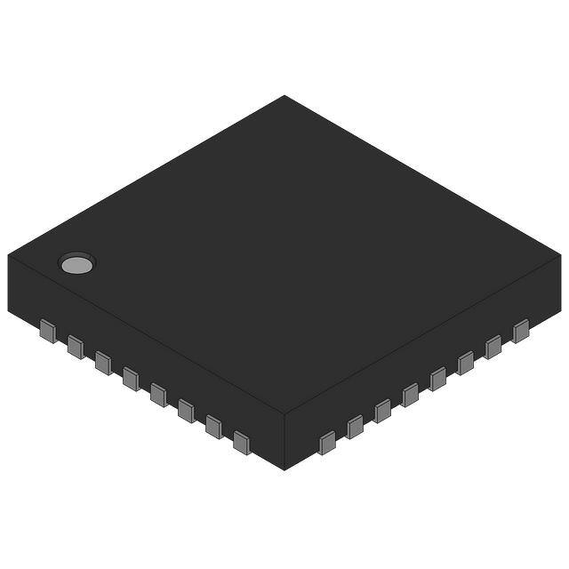


 工商网监
湘ICP备2023018690号
工商网监
湘ICP备2023018690号
