Evaluates: MAX17559
MAX17559 Evaluation Kit
General Description
The MAX17559 EV kit is a proven design to evaluate
the dual synchronous step-down regulator that provides
independent 3.3V and 5V outputs capable of driving 8A
and 15A loads from the 6V to 60V input-voltage range.
Operating the two regulators 180° out-of-phase significantly
reduces the peak input ripple current, allowing the use
of smaller, less expensive components, while minimizing
parts count. The EV kit features adjustable input undervoltage
lockout, soft-start/stop time, and current-limit threshold,
as well as selectable PWM/DCM modes, foldback/latchoff
current limit, and independent open-drain PGOOD signals.
By disabling channel 2, the evaluation kit is capable of
operating from a lower input supply (4.5V to 60V), providing
a single 3.3V output driving up to 15A.
Benefits and Features
●● 6V to 60V Input Range
●● Output Rails: VOUT1: 3.3V/15A, VOUT2: 5V/8A
●● 150kHz Switching Frequency
●● Independent Enable Inputs
●● Independent Adjustable Soft-Start Time
●● Configurable Tracking Operation
●● Selectable PWM/DCM Modes of Operation
●● Fixed 180° Out-of-Phase Operation
●● Selectable Foldback/Latchoff Current Limit
●● Programmable Current-Limit Threshold
●● Independent PGOOD Outputs
●● Overcurrent, Overvoltage, and Overtemperature
Protection
Quick Start
Required Equipment
●●
MAX17559 EV kit
●●
4.5V to 60V, 15A DC power supply
●●
Loads capable of sinking 8A and 15A
●●
Two digital voltmeters (DVM)
Procedure
The EV kit is fully assembled and tested. Follow the steps
below to verify board operation. Caution: Do not turn on
the power supply until all connections are completed.
1) Set the power supply voltage to 24V and ensure that
the DC power supply is disabled.
2) Set one load to 8A and the other load to 15A. Disable
the loads in the case of electronic loads (leave the
loads unconnected in case of resistor loads. Ensure
that the resistor power ratings are high enough to
dissipate the output voltages).
3) Connect the positive terminal of the power supply to
the VIN connector and the negative terminal to the
PGND connector, which is nearest to VIN connector.
4) Connect one digital voltmeter across the VOUT1
connector and the nearest PGND connector, with
the positive terminal of the DVM connected to the
VOUT1 connector.
5) Connect the other digital voltmeter across the
VOUT2 connector and the nearest PGND connector,
with the positive terminal of the DVM connected to
the VOUT2 connector.
●● Proven PCB Layout
6) Verify that the shunts are connected between pins
1-2 of the JU1 and JU2 jumpers to select default settings
of the EV kit
●● Fully Assembled and Tested
7) Turn on the DC power supply.
8) Verify that the digital voltmeters display the expected
voltages (3.3V±1% on VOUT1 and 5V±1% on
VOUT2).
Ordering Information appears at end of data sheet.
9) Enable the electronic load (connect the load in the
case of resistor load).
10) Verify that the voltmeters display the expected voltages (3.3V±1% on VOUT1 and 5V±1% on VOUT2).
19-7696; Rev 0; 6/15
�MAX17559 Evaluation Kit
Evaluates: MAX17559
Detailed Description of Hardware
time of VOUT1 and VOUT2 are calculated based on the
following equation:
The MAX17559 EV Kit provides dual 3.3V/15A and 5V/8A
outputs from a 6V to 60V input supply. By disabling channel
2, the EV kit provides a 3.3V output to drive up to 15A
from a low 4.5V to 60V input voltage. The EV Kit is preset
to 150kHz and operates 180° out-of-phase for optimum
efficiency and component size.
t=
SS_ C SS _×
The default soft-start/stop time of VOUT1 or VOUT2 is
approximately 10.8ms at 68nF soft-start/stop capacitor.
The EV kit implements an optional sub-circuit, R13–R18,
R28, D7, and JU1, JU2 to enable/disable the output at
a desired input UVLO, as well as soft-start/stop power
sequence. Resistors R35 and R36 are selected different
values to configure the EV kit operating in DCM/PWM mode
and foldback/latchoff, current-limit mode, respectively.
Enable/Undervoltage-Lockout
Level (EN_)
The device can be independently started up or shut
down by manipulating the EN1 and EN2 pins. Leave EN_
unconnected for a default enable controller. Place shunts
across pins 1-2 of JU1 and JU2 to enable each controller through the input UVLO formed by resistor-dividers.
Connect a resistor-divider from VIN to EN_ and EN_ to
GND to program the UVLO threshold for the corresponding controller. The EN_ pin can be programmed to 1.25V
(typ) to detect UVLO at a desired input voltage to enable/
disable the corresponding controller with 50mV (typ)
hysteresis. Place jumpers across pins 2-3 of JU1 and JU2
to disable the controllers. Table 1 shows all configurations
of jumpers to enable/disable each of controllers.
Configuring the Output Voltages (VOUT1, VOUT2)
The device output voltages (VOUT1 and VOUT2) can be
adjusted between 0.8V to 24V through sets of feedback
resistor-dividers R19,R20 and R23,R24 by the following
formula:
=
R20
R19
R23
=
and R24
VOUT1
VOUT2
(
(
− 1)
− 1)
0.8
0.8V
5µA
0.8
Please refer to MAX17559 IC data sheet to select the R19
and R23 values, changing compensation components, as
well as output capacitors for setting new output voltages.
Select R14 (R18 for OUT2) below 10K and calculate R13
(R17) based on the following equation:
Soft-Start/Stop (SS_)
R13 =
The device offers an SS_ pin to connect a capacitor to GND
to adjust the soft-start/stop time during startup and shutdown. An internal 5µA current source charges/discharges
the capacitor at the SS_ pin, providing a linear ramping
voltage for output voltage reference. The soft-start/stop
R14 × (VINUVLO − 1.25)
1.25
where VINUVLO is the input voltage at which the controller
is required to turn on.
Table 1. Enable Control (JU1, JU2)
JUMPER
SHUNT POSITION
EN
MAX17558 OUTPUT
Not installed
Unconnected
Enabled
1-2
Connected to the midpoint of
input UVLO divider
Enabled, UVLO level is set by the
resistor divider from VIN to GND.
2-3
Connected to GND
Disabled
Not installed
Unconnected
Enabled
1-2
Connected to the mid-point of
input UVLO divider
Enabled, UVLO level is set by the
resistor divider from VIN to GND.
2-3
Connected to GND
Disabled
JU1
JU2
www.maximintegrated.com
Maxim Integrated │ 2
�MAX17559 Evaluation Kit
Mode Selection (SKIP)
The SKIP pin allows the user to select between the
PWM and DCM modes of operation. Set R36 = 0Ω to
select constant-frequency PWM mode operation. Choose
100kΩ to operate in DCM mode.
Fixed Phase-Shift Between Controllers
The two controllers of the dual switching regulator operate
at a fixed 180° out-of-phase that interleaves the current
pulses from the switches and reduces overlap time where
they combine. The result is a significant reduction in total
RMS input current, allowing for less expensive input
capacitors to be used, reducing shielding requirements for
EMI, and improving operating efficiency.
Current-Limit Threshold Selection
The EV kit includes current-limit resistors (R12 and R22)
that can be modified to program current-limit thresholds
for controllers 1 and 2. The peak current limit of each
controller can be programmed independently by selecting different values for R12 and R22. Note that changing
R12 and R22 affect the stability and current-sense signal
across the current sense pins. Refer to the Current Limit
Programming (ILIM_) and Current Sensing sections of
MAX17559 IC data sheet for calculating R12, R22 and the
current sense resistor values.
www.maximintegrated.com
Evaluates: MAX17559
Switching Frequency
The EV kit is set to a 150kHz switching frequency by
R14. Change the value of R14 to set a different switching
frequency between 100kHz to 2200kHz. Use the following
equation to calculate R14 when reconfiguring the switching
frequency:
R RT =
(f SW + 133)
8.8
where fSW is in kHz and R14 is in kΩ.
When reconfiguring the EV kit switching frequency, it
might be necessary to change the values of the loopcompensation-network components. Refer to the Loop
Compensation section of the MAX17559 IC data sheet for
computing new compensation component values.
Power-Good Outputs
The EV kit provides power-good output test points
PGOOD1 and PGOOD2 to monitor the PGOOD1 and
PGOOD2 signals. The PGOOD signals are pulled-up to
VCCINT by R26 and R27. PGOOD1 and PGOOD2 are
high when VOUT1 and VOUT2, respectively, are above
90% and below 110% of their programmed output voltages. When VOUT1 and VOUT2 are below 90% or above
110% of their programmed output voltages, PGOOD1 and
PGOOD2 are low.
Maxim Integrated │ 3
�MAX17559 Evaluation Kit
Evaluates: MAX17559
EV Kit Performance Report
90
90
80
80
70
70
60
50
VIN = 24V VIN = 36V
VIN = 12V
40
20
0
5000
10000
0
15000
OUTPUT (mA)
EFFICIENCY (%)
50
40
VIN = 36V
VIN = 24V
20
2000
4000
6000
8000
COINCIDENT TRACKING AT STARTUP
VIN = 24V, VOUT1 = 3.3V, IOUT1 = 15A,
VOUT2 = 5V, IOUT2 = 8A
toc10
VOUT2
1V/div
VOUT2
1V/div
VOUT1
1V/div
VOUT1
1V/div
IOUT1
5A/div
IOUT1
5A/div
IOUT2
5A/div
IOUT2
5A/div
fSW = 150kHz
10
0
0
OUTPUT (mA)
STARTUP FROM ENABLE
VIN = 24V, VOUT1 = 3.3V, IOUT1 = 15A,
VOUT2 = 5V, IOUT2 = 8A toc08
60
VIN = 12V
VIN = 24V
FSW=150kHz
20
70
VIN = 36V
80
70
80
30
85
75
fSW = 150kHz
VIN = 12V
90
90
OUTPUT (mA)
EFFICIENCY vs. OUTPUT CURRENT
VOUT = 5V, DCM MODE
toc04
100
VIN = 36V
10
fSW = 150kHz
0
VIN = 24V
40
30
toc03
95
50
20
EFFICIENCY vs. OUTPUT CURRENT
VOUT = 5V, PWM MODE
100
VIN = 12V
60
30
10
EFFICIENCY vs. OUTPUT CURRENT
VOUT = 3.3V, DCM MODE
toc02
100
EFFICIENCY (%)
EFFICIENCY (%)
100
EFFICIENCY (%)
EFFICIENCY vs. OUTPUT CURRENT
VOUT = 3.3V, PWM MODE
toc01
10
100
10ms/div
10ms/div
1000
OUTPUT (mA)
STARTUP INTO PREBIASED OUTPUT
VIN = 24V, VOUT1 = 3.3V, IOUT1 = 0A,
VOUT2 = 5V, IOUT2 = 0A
toc09
LOAD TRANSIENT RESPONSE
VIN = 24V, VOUT1 = 3.3V, IOUT1 = 7.5A to 15A
PWM MODE
toc13
LOAD TRANSIENT RESPONSE
VIN = 24V, VOUT2 = 5V, IOUT2 = 4A to 8A
toc16
PWM MODE
1V/div
100mV/div
AC-COUPLED
VOUT1
100mV/div
AC-COUPLED
VOUT2
1V/div
VOUT1
IOUT2
IOUT1
2V/div
EN
10ms/div
www.maximintegrated.com
5A/div
5A/div
400µs/div
400us/div
Maxim Integrated │ 4
�MAX17559 Evaluation Kit
Evaluates: MAX17559
EV Kit Performance Report (continued)
120
40
30
90
30
20
60
20
60
10
30
10
30
0
0
0
0
PHASE
-10
GAIN
-20
-30
-60
CROSSOVER FREQUENCY = 10 kHz
PHASE MARGIN = 64.7◦
-40
-50
-30
1k
10k
FREQUENCY (Hz)
www.maximintegrated.com
100k
GAIN (dB)
50
40
GAIN (dB)
CLOSED-LOOP BODE PLOT
VIN = 24V, VOUT = 3.3V, IOUT = 15A
150
PHASE MARGIN (°)
50
toc21
-90
-30
-120
-40
-150
-50
90
-30
GAIN
-20
150
120
PHASE
-10
toc22
-60
CROSSOVER FREQUENCY = 14.1 kHz
PHASE MARGIN = 64.7◦
PHASE MARGIN (°)
CLOSED-LOOP BODE PLOT
VIN = 24V, VOUT = 5V, IOUT = 8A
-90
-120
1k
10k
100k
-150
FREQUENCY (Hz)
Maxim Integrated │ 5
�MAX17559 Evaluation Kit
Evaluates: MAX17559
Component Suppliers
SUPPLIER
WEBSITE
Wurth Elektronik
www.we-online.com
Renesas Electronics
am.renesas.com
Murata Americas
www.murata.com
Panasonic Electronic Components
www.panasonic.com/industrial
Vishay Dale
www.vishay.com
TDK Corp.
www.tdk.com
Rubycon Corp.
www.rubycon.com
TT Electronics/Welwyn
www.welwyn-tt.com
Note: Indicate that you are using the MAX17559 when contacting these component suppliers.
Component List, PCB Files and
Schematic
See the following links for component information, PCB
files, and schematics:
●● MAX17559 EV BOM
Ordering Information
PART
TYPE
MAX17559EVKIT#
EV kit
#Denotes RoHS compliant.
●● MAX17559 EV PCB Files
●● MAX17559 EV Schematics
www.maximintegrated.com
Maxim Integrated │ 6
�MAX17559 Evaluation Kit
Evaluates: MAX17559
Revision History
REVISION
NUMBER
REVISION
DATE
0
6/15
DESCRIPTION
Initial release
PAGES
CHANGED
—
For pricing, delivery, and ordering information, please contact Maxim Direct at 1-888-629-4642, or visit Maxim Integrated’s website at www.maximintegrated.com.
Maxim Integrated cannot assume responsibility for use of any circuitry other than circuitry entirely embodied in a Maxim Integrated product. No circuit patent licenses
are implied. Maxim Integrated reserves the right to change the circuitry and specifications without notice at any time.
Maxim Integrated and the Maxim Integrated logo are trademarks of Maxim Integrated Products, Inc.
© 2015 Maxim Integrated Products, Inc. │ 7
�6
5
OUT
OUT
PGOOD2
VCCINT
VCCEXT
IN
OUT
PGOOD1
IN
EN2
1
2
IN
EN1
IN
VOUT2
IN
VCC_CIRCLE
3
IN
VOUT1
4
VCCEXT
7
VCCINT
PGOOD1
8
VIN
C28
D
0.015UF
C29
R19
D
R8
270PF
46.4K
2.2
R26
R21
VIN11
10K
5.11K
+
C26
R20
OUT
0.068UF
14.7K
VCCINT
2
4
G S
L1
3.1UH
2
2
6
GND
PGND
21
7
EN1
DL2
18
8
EN2
LX2
16
4
N4
D
4
G S
1
2
3
1
2
3
4
1
A
G S
D2
15
14
13
12
11
10
9
C
0.068UF
A
IN
4
1
+
330UF
1
C18
10UF
10UF
PGND6
R2
2
VOUT2
0.004
D
86.6K
C33
R24
16.5K
CS2-
C7
4.7UF
C8
4.7UF
C9
4.7UF
A
C35
4.7UF
OUT
VCCINT
OUT
R23
CS2+
VIN
C6
4.7UF
VOUT2
2
N5
RJK0651DPB-00#J5
VOUT2
10K
PGOOD2
EN2
1
PGND2
C17
5
IN
OPEN
G S
CS2- CS2+
R28
B
VOUT21
0
R27
0.033UF
OUT
3
PGND3
VCCINT
D4
R5
C30
R17
330UF
OUT
R25
C
0
470PF
R18
C16
OUT
C27
C31
OPEN
10UF
C22
9.09K
JU2
C15
C
0
A
R31
VIN
OPEN
C14
1UF
1000PF
150
PGOOD2
C13
10UF
2K
R10
A
L2
6.8UH
R33
C25
1
1
2
3
OPEN
3
R14
OPEN
R7
D6
C32
N6
RJK0653DPB-00#J5
3
17
5
DH2
BST2
OPEN
2
C12
330UF
D
PGOOD2
SS2
COMP2
FB2
CS2+
JU1
CS2-
R15
EN1
1
PGOOD2
C11
330UF
2
2
A
1
2
3
OPEN
R13
C
OPEN
OUT
C10
330UF
PGND1
A
R16
OPEN
D7
D1
G S
VIN
B
1
3
RJK0653DPB-00#J5
D
+
N3
VOUT1
C
RJK0653DPB-00#J5
0
R1
0.002
A
D5
1
23
A
SKIP
A
2
DL1
VOUT11
1
2
3
0
C
MAX17559
5
R6
0
0
R36
1
2
3
25
5
LX1
ILIMSEL
5
4
VCC_CIRCLE
G S
R29
R35
VOUT1
VCC_CIRCLE
0
182K
VCCINT
4
CS1-
RJK0651DPB-00#J5
D
+
26
N2
RJK0651DPB-00#J5
D
R4
CS1+
2
DH1
ILIM2
IN
C21
1UF
C
N1
2
3
A
+
19
VCCINT
0
VCCINT
D3
C
1
20
VCCEXT
RT
R30
1
24
R3
31.6K
R12
PGND4
C34
4.7UF
+
BST1
C5
4.7UF
2
22
C4
4.7UF
2
IN
C3
4.7UF
1
2
C1
220UF
VCCEXT
1
27
PGOOD1
C2
4.7UF
VIN
0
R11
VCCINT
PGND5
5
28
ILIM1
CS1-
PGOOD2
C19
0.1UF
5
29
SS1
1
1000PF
VCC_CIRCLE
C
CS1+
PGOOD1
VIN
C24
150
CS1-
32
EN2
EN1
10UF
30
182K
COMP1
R22
31
R34
2K
FB1
R9
IN
GND
C20
U1
CS1+
VIN
1
C23
2.2UF
R32
OPEN
PROJECT TITLE:
1
MAX17559 EVALUATION KIT
2
DRAWING TITLE:
OPEN
SIZE
DATE:
HARDWARE NUMBER:
B -
ENGINEER:
-
05/19/2015
DRAWN BY:
REV:
-
A
TEMPLATE REV:
SHEET 2 OF 2
1.5
8
7
6
5
4
3
2
1
�BILL OF MATERIALS (BOM) Revision 5/15
Designation
C32,C33
Qty Description
220uF,63V
1
Panasonic Electronic EEVFK1J221Q
CAP CER 4.7UF 80V 10% X7R 1210
10
Murata GRM32ER71K475KE14L
330uF,9mΩ, 6.3V
5
Panasonic Electronic 6TPF330M9L
10uF,10V,X7R,1210,10%
4
Murata GRM32DR71A106KA01L
10uF,10V,X7R,1210,10%
0
Murata GRM32DR71A106KA01L
CAP CER 0.1UF 100V 10% X7R 0603
1
Murata GRM188R72A104KA35D
10uF,10V,X7R,0805,10%
1
Murata GRM21BR71A106KE51L
1uF,10V(16V),10%,X7R
2
Murata GRM188R71A105KA61J
Murata GRM188R71A225KE15
1nF,50V,1%,NP0
2
Murata GRM1885C1H102FA01J
68nF,25V,X7R,10%
2
Murata GRM188R71E683KA01
Murata GRM188R71E153KA01
270pF,50V,C0G,2%(5%)
1
Murata GRM1885C1H271GA01
(GRM1885C1H271JA01)
33nF,25V,X7R,10%
1
Murata GRM188R71E333KA01
470pF,50V,C0G,55
1
Murata GRM1885C1H471JA01
OPEN
0
R1
1
R2
1
R3,R4,R5,R6,R7, R29, R30, R31, R35, R36
10
R8
R11
R13,R14,R15,R16,R17,R18, R28, R32
R19
R20
R21
R23
R24
R25
R26, R27
R33, R34
1
1
0
1
1
1
1
1
1
2
2
L1
1
L2
1
C1
C2-C9, C34, C35
C10,C11,C12, C15, C16
C13,C14,C17, C18
C18
C19
C20
C21,C22
C24,C25
C26,C27
C29
C30
C31
2mΩ, 1W,1%
Rohm Semiconducto PMR25HZPFV2L00
4mΩ, 1W,1%
Rohm Semiconducto PMR25HZPFV4L00
0Ω
2.2Ω
31.6KΩ
OPEN
46.4KΩ
14.7KΩ
5.11KΩ
86.6KΩ
16.5KΩ
9.09KΩ
10KΩ
2KΩ
3.1uH, 15%,26A,2.09mΩ
Wurth Electronics 7443630310
6.8uH,20%,18.5A,4.1mΩ
Wurth Electronics 7443556680
�N1,N2,N5
3
N3, N4, N6
3
D1,D2
2
D3,D4
2
D5,D6
D7
0
0
U1
1
VIN,PGND,VOUT1,PGND,VOUT2,EN1,EN2,PGOO 11
JU1, JU2
6
VIN,PGND,VOUT1,PGND,VOUT2,PGND
2
CONN JUMPER SHORTING TIN
2
60V,25A,13mΩ
Renesas RJK0651DPB-00#J5
60V,45A,4.5mΩ
Renesas RJK0653DPB-00#J5
DIODE SCHOTTKY 60V 5A TO277A
Vishay Semiconductor SS5P6-M3/86A
DIODE SCHOTTKY 100V 250MA
NXP Semiconductors BAT46WJ,115
Open
Open
MAX17559
Maxim MAX17559ACJ+
20G tinned copper Bus wire formed into “U”
shaped loops (0.25” off the PC board)
3-pin header ( 0.1” pitch)
Sullins PREC003SAAN-RC
Non -Insulate Jack
Keystone Electronics 575-4
Shunts, 0.1" Pitch
Sullins STC02SYAN
�This document contains information considered proprietary,
and shall not be reproduced wholly or in part,
nor disclosed to others without specific written permission.
HARDWARE NAME:MAX17559_EVKIT_A
HARDWARE NUMBER:
DATE: 05/28/2015
ODB++/GERBER:
SILK_TOP
PGOOD1
DESIGNER:
VCCINT
ENGINEER:
L1
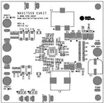
MAX17559 EVKIT
VOUT1
3.3V
1-888-629-4642
@15A
www.maximintegrated.com
R29
REV-A
05/15 SJ
R4
C12
C11
C10
R1
C14 C13
D1
N4
N1
N3
N2
VIN
D3
R6
C21
R34
R22
R21
C29
R19
R20
C28 C26
PGND
C24
C35
R3
U1
C9
R9
C32
C23
C27
R23
R24
R25
C31
PGND
C22
N6
R5
N5
C1
C15
C17
C16
C18
C6
D2
C30
R2
VOUT2
PGND
JU1
JU2
VCCEXT
PGOOD2
EN2
GND
L2
EN1
5V @8A
C7
D4
R33
R7
R31
R10
C8
C20
C25
C33
40V max.
C19
R30
R32
R11
R12
1/6
�This document contains information considered proprietary,
and shall not be reproduced wholly or in part,
nor disclosed to others without specific written permission.
HARDWARE NAME:MAX17559_EVKIT_A
HARDWARE NUMBER:
ENGINEER:
DESIGNER:
DATE: 05/28/2015
ODB++/GERBER:
2/6
TOP
�This document contains information considered proprietary,
and shall not be reproduced wholly or in part,
nor disclosed to others without specific written permission.
HARDWARE NAME:MAX17559_EVKIT_A
HARDWARE NUMBER:
ENGINEER:
DESIGNER:
DATE: 05/28/2015
ODB++/GERBER:
3/6
SGND
�This document contains information considered proprietary,
and shall not be reproduced wholly or in part,
nor disclosed to others without specific written permission.
HARDWARE NAME:MAX17559_EVKIT_A
HARDWARE NUMBER:
ENGINEER:
DESIGNER:
DATE: 05/28/2015
ODB++/GERBER:
4/6
PGND
�This document contains information considered proprietary,
and shall not be reproduced wholly or in part,
nor disclosed to others without specific written permission.
HARDWARE NAME:MAX17559_EVKIT_A
HARDWARE NUMBER:
ENGINEER:
DESIGNER:
DATE: 05/28/2015
ODB++/GERBER:
5/6
BOTTOM
�This document contains information considered proprietary,
and shall not be reproduced wholly or in part,
nor disclosed to others without specific written permission.
HARDWARE NAME:MAX17559_EVKIT_A
HARDWARE NUMBER:
ENGINEER:
DESIGNER:
DATE: 05/28/2015
ODB++/GERBER:
SILK_BOT
R26
C34
C5
D5
R36 R35
C4
C3
D6
R27
C2
R18
R28
R17
D7
R15
R8
R14
R13
R16
6/6
�


 工商网监
湘ICP备2023018690号
工商网监
湘ICP备2023018690号
