Click here to ask about the production status of specific part numbers.
MAX17577, MAX17578
4.5V to 60V, 1A High-Efficiency, Synchronous,
Inverting Output DC-DC Converters
General Description
Benefits and Features
The Himalaya series of voltage regulator ICs, power modules, and chargers enable cooler, smaller, and simpler
power-supply solutions. The MAX17577 and MAX17578
are high-efficiency, high-voltage, inverting, Himalaya synchronous DC-DC converters with integrated MOSFETs
and internal compensation. The devices generate output
voltages (VOUT) from -0.9V to -36V and can deliver up to
1A of load current from a wide 4.5V to (60V - |VOUT|) input-voltage range.
● Reduces External Components and Total Cost
• Synchronous Operation
• All-Ceramic Capacitors, Compact Layout
• Internal Loop Compensation
• System Ground Referenced I/O Pins (EN/UVLO,
RESET)
The devices feature peak current-mode control architecture. The MAX17577 operates in continuous conduction
mode (CCM) at all loads; thus, providing a constant frequency operation. The MAX17578 operates in discontinuous conduction mode (DCM) for superior efficiency at light
loads. Low minimum on-time allows higher switching frequencies and small solution sizes.
The devices allow the EN/UVLO, RESET, and RT/SYNC
pins to be driven by signals that are referenced to system
ground, eliminating the need for external-level shifter circuits. The feedback-voltage regulation accuracy is ±1.3%
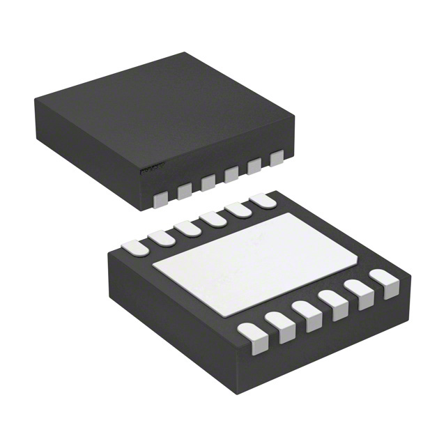
over a wide -40°C to +125°C temperature range. The devices are available in a compact 12-pin (3mm x 3mm)
TDFN package. Simulation models are available.
Applications
●
●
●
●
●
●
Industrial Control Power Supply
General-Purpose Point-of-Load
Gate-Drive Circuits
Motion Control
Wall-Transformer Regulation
High-Voltage, Single-Board System
● Flexibility to Support Multiple Rails in a System
• Adjustable Output Voltage Range from -0.9V to
-36V
• Wide 4.5V to (60V - |VOUT|) Input-Voltage Range
• Up to 1A Output Current
• 400kHz to 2.2MHz Adjustable Frequency with
External Clock Synchronization
● Reduces Power Dissipation
• 90.6% Peak Efficiency
• DCM for Superior Light-Load Efficiency
• 6.2μA Shutdown Current
● Operates Reliably in Adverse Industrial Environments
• Hiccup-Mode Overload Protection
• Adjustable Soft-Start
• Monotonic Startup with Prebiased Output Voltage
• Built-In Output-Voltage Monitoring with RESET
• Programmable EN/UVLO Threshold
• Overtemperature Protection
• Wide -40°C to +125°C Ambient Operating
Temperature Range/ -40°C to +150°C Junction
Temperature Range
Ordering Information appears at end of data sheet.
Simplified Application Circuit
VIN
IN
RESET
EN/UVLO
BST
MAX17577/
MAX17578
RT/SYNC
LX
VCC
FB
SS
GND
SOUT EP
FB
FB
OUT
VOUT
19-100840; Rev 0; 10/20
�MAX17577, MAX17578
4.5V to 60V, 1A High-Efficiency, Synchronous,
Inverting Output DC-DC Converters
Absolute Maximum Ratings
IN, GND, EN/UVLO to OUT.................................... -0.3V to +65V
IN to GND ............................................................... -0.3V to +65V
EN/UVLO to GND...........................................-0.3V to VIN + 0.3V
RESET to GND...................................................... -0.3V to +6.5V
LX to OUT ................................................... -0.3V to (VIN + 0.3V)
RESET, BST to OUT .............................................. -0.3V to +70V
BST to LX .............................................................. -0.3V to +6.5V
BST to VCC............................................................. -0.3V to +65V
FB, SS, VCC to SOUT ........................................... -0.3V to +6.5V
RT/SYNC to SOUT................................................... -2V to +6.5V
OUT to SOUT ........................................................ -0.3V to +0.3V
LX Total RMS Current............................................................1.6A
Output Short-Circuit Duration......................................Continuous
Continuous Power Dissipation (Multilayer Board) (TA = +70°C,
derate 24.4mW/°C above +70°C) ................................1951.2mW
Operating Temperature Range (Note 1) .............-40°C to +125°C
Junction Temperature ....................................................... +150°C
Storage Temperature Range ..............................-65°C to +150°C
Lead Temperature (soldering, 10s)................................... +300°C
Soldering Temperature (reflow) ........................................ +260°C
Note 1: Junction temperature greater than +125°C degrades operating lifetimes.
Stresses beyond those listed under “Absolute Maximum Ratings” may cause permanent damage to the device. These are stress ratings only, and functional operation of the
device at these or any other conditions beyond those indicated in the operational sections of the specifications is not implied. Exposure to absolute maximum rating conditions for
extended periods may affect device reliability.
Package Information
TDFN
Package Code
TD1233+1C
Outline Number
21-0664
Land Pattern Number
90-0397
THERMAL RESISTANCE, FOUR-LAYER BOARD (Note 2)
Junction-to-Ambient (θJA)
33ºC/W
Junction-to-Case Thermal Resistance (θJC)
8.5ºC/W
For the latest package outline information and land patterns (footprints), go to www.maximintegrated.com/packages.
Note that a “+”, “#”, or “-” in the package code indicates RoHS status only. Package drawings may show a different
suffix character, but the drawing pertains to the package regardless of RoHS status.
Note 2: Package thermal resistance was obtained using the MAX17578 evaluation kit with no airflow
Electrical Characteristics
(VIN = VEN/UVLO = 24V, CVCC = 2.2μF, VFB = 1V, RT/SYNC = LX = SS = RESET = Open, VBST to VLX = 5V, VGND = VSOUT = VOUT
= 0V, TA = -40°C to +125°C. Typical values are at TA = +25°C. All voltages are referenced to SOUT, unless otherwise noted.) (Note 3)
PARAMETER
SYMBOL
CONDITIONS
MIN
TYP
MAX
UNITS
60 |VOUT|
V
10
μA
INPUT SUPPLY (IN)
Input-Voltage Range
Input-Shutdown Current
No-Load Input Current
VIN_GND
IIN-SH
INO_LOAD
(Referred to GND)
4.5
VEN/UVLO = 0V (referred to GND),
shutdown mode
6.2
MAX17577, Normal Switching Mode
6.3
MAX17578
1.5
2
mA
ENABLE/UNDERVOLTAGE LOCKOUT (EN/UVLO)
EN/UVLO Threshold
EN/UVLO InputLeakage Current
www.maximintegrated.com
VENR
VEN/UVLO rising (referred to GND)
1.165
1.229
1.275
VENF
VEN/UVLO falling (referred to GND)
1.04
1.09
1.14
VEN/UVLO = GND, TA = +25°C
-50
0
+50
IENLKG
V
nA
Maxim Integrated | 2
�MAX17577, MAX17578
4.5V to 60V, 1A High-Efficiency, Synchronous,
Inverting Output DC-DC Converters
Electrical Characteristics (continued)
(VIN = VEN/UVLO = 24V, CVCC = 2.2μF, VFB = 1V, RT/SYNC = LX = SS = RESET = Open, VBST to VLX = 5V, VGND = VSOUT = VOUT
= 0V, TA = -40°C to +125°C. Typical values are at TA = +25°C. All voltages are referenced to SOUT, unless otherwise noted.) (Note 3)
PARAMETER
SYMBOL
CONDITIONS
MIN
TYP
MAX
1mA < IVCC < 15mA
4.75
5
5.25
6V ≤ VIN ≤ 60V; IVCC = 1mA
4.75
5
5.25
25
60
UNITS
LDO (VCC)
VCC Output Voltage
VCC Current Limit
VCC Dropout
VCC UVLO
VCC
IVCC_MAX
VCC = 4.3V, VIN = 6.5V
VCC_DO
VIN = 4.5V, IVCC=15mA
VCC_UVR
VCC rising
4.05
4.2
4.3
VCC_UVF
VCC falling
3.65
3.8
3.9
V
100
mA
0.35
V
V
HIGH-SIDE AND LOW-SIDE MOSFETS
High-Side nMOSFET
On-Resistance
RDS-ONH
ILX = 0.3A, Sourcing
330
660
mΩ
Low-Side nMOSFET
On-Resistance
RDS-ONL
ILX = 0.3A,Sinking
163
325
mΩ
LX Leakage Current
ILXLKG
+2
μA
VLX = (VOUT + 1V) to (VIN - 1V), TA =
+25°C
-2
VSS = 0.5V
4.7
5
5.3
μA
0.888
0.9
0.912
V
+50
nA
SOFT-START (SS)
Charging Current
ISS
FEEDBACK (FB)
FB Regulation Voltage
VFB-REG
FB Input-Bias Current
IFB
0 ≤ VFB ≤ 1V, TA = +25°C
-50
CURRENT LIMIT
Peak Current-Limit
Threshold
Runaway Current-Limit
Threshold
Sink Current-Limit
Threshold
IPEAK-LIMIT
2.15
2.4
2.65
A
IRUNAWAY-
2.3
2.65
3
A
LIMIT
ISINK-LIMIT
MAX17577
-0.9
MAX17578
0
A
SWITCHING FREQUENCY AND EXTERNAL CLOCK SYNCHRONIZATION (RT/SYNC)
Switching Frequency
fSW
Minimum On-Time
tON_MIN
Minimum Off-Time
tOFF_MIN
LX Dead Time
VFB Hiccup Threshold
SYNC FrequencyCapture Range
www.maximintegrated.com
525
600
675
RRT/SYNC = 6.81kΩ
365
400
425
RRT/SYNC = 10.5kΩ
565
600
635
RRT/SYNC = 43.2kΩ
1980
2200
2420
60
80
ns
140
150
160
ns
0.55
0.58
tLX-DT
VFB-HICF
Hiccup Timeout
Bias Current
RRT/SYNC = Open
5
VFB Falling
(Note 4)
IRT_BIAS
fSW set by RRT/SYNC
1.1 x
fSW
kHz
ns
0.61
V
32768
cycles
60
μA
1.4 x
fSW
kHz
Maxim Integrated | 3
�MAX17577, MAX17578
4.5V to 60V, 1A High-Efficiency, Synchronous,
Inverting Output DC-DC Converters
Electrical Characteristics (continued)
(VIN = VEN/UVLO = 24V, CVCC = 2.2μF, VFB = 1V, RT/SYNC = LX = SS = RESET = Open, VBST to VLX = 5V, VGND = VSOUT = VOUT
= 0V, TA = -40°C to +125°C. Typical values are at TA = +25°C. All voltages are referenced to SOUT, unless otherwise noted.) (Note 3)
PARAMETER
SYNC Pulse-Width
SYMBOL
CONDITIONS
tSYNC
VIH
SYNC Duty-Cycle
Range
TYP
MAX
100
At RT/SYNC Pin (Note 5)
UNITS
ns
VRT/
SYNC +
0.2
SYNC Threshold
VIL
MIN
VRT/
At RT/SYNC Pin (Note 5)
V
SYNC -
0.2
DSYNC
10
90
%
SYSTEM GROUND (GND)
GND Current
IGND
Sourcing
10
μA
RESET (REFERRED TO GND)
RESET Output Level
Low
RESET Output-Leakage
Current
VRESETL
IRESETLKG
IRESET = 10mA (Referred to GND)
TA = TJ = +25°C, VRESET = 5.5V
-0.1
0.4
V
+0.1
μA
FB Threshold for
RESET Deassertion
VFB-OKR
VFB Rising
93.8
95
97.8
%
FB Threshold for
RESET Assertion
VFB-OKF
VFB Falling
90.5
92
94.6
%
RESET Delay after FB
reaches 95% regulation
1024
Cycles
THERMAL SHUTDOWN
Thermal Shutdown
Rising Threshold
TSHDNR
165
°C
Thermal Shutdown
Hysteresis
TSHDNHY
10
°C
Note 3: Electrical specifications are production tested at TA = +25ºC. Specifications over the entire operating temperature range are
guaranteed by design and characterization.
Note 4: See the Overcurrent Protection (OCP)/Hiccup Mode section for more details
Note 5: VRT/SYNC = IRT_BIAS × RRT/SYNC. See the Switching Frequency and External Clock Synchronization (RT/SYNC) section for
more details.
www.maximintegrated.com
Maxim Integrated | 4
�MAX17577, MAX17578
4.5V to 60V, 1A High-Efficiency, Synchronous,
Inverting Output DC-DC Converters
Typical Operating Characteristics
(VGND = 0V, CVCC = 2.2μF, CBST = 0.1μF, CSS = 5600pF, TA = -40°C to +125°C, unless otherwise noted. Typical values are at TA =
+25°C. All voltages are referenced to GND, unless otherwise noted.)
www.maximintegrated.com
Maxim Integrated | 5
�MAX17577, MAX17578
4.5V to 60V, 1A High-Efficiency, Synchronous,
Inverting Output DC-DC Converters
Typical Operating Characteristics (continued)
(VGND = 0V, CVCC = 2.2μF, CBST = 0.1μF, CSS = 5600pF, TA = -40°C to +125°C, unless otherwise noted. Typical values are at TA =
+25°C. All voltages are referenced to GND, unless otherwise noted.)
www.maximintegrated.com
Maxim Integrated | 6
�MAX17577, MAX17578
4.5V to 60V, 1A High-Efficiency, Synchronous,
Inverting Output DC-DC Converters
Typical Operating Characteristics (continued)
(VGND = 0V, CVCC = 2.2μF, CBST = 0.1μF, CSS = 5600pF, TA = -40°C to +125°C, unless otherwise noted. Typical values are at TA =
+25°C. All voltages are referenced to GND, unless otherwise noted.)
www.maximintegrated.com
Maxim Integrated | 7
�MAX17577, MAX17578
4.5V to 60V, 1A High-Efficiency, Synchronous,
Inverting Output DC-DC Converters
Typical Operating Characteristics (continued)
(VGND = 0V, CVCC = 2.2μF, CBST = 0.1μF, CSS = 5600pF, TA = -40°C to +125°C, unless otherwise noted. Typical values are at TA =
+25°C. All voltages are referenced to GND, unless otherwise noted.)
www.maximintegrated.com
Maxim Integrated | 8
�MAX17577, MAX17578
4.5V to 60V, 1A High-Efficiency, Synchronous,
Inverting Output DC-DC Converters
Typical Operating Characteristics (continued)
(VGND = 0V, CVCC = 2.2μF, CBST = 0.1μF, CSS = 5600pF, TA = -40°C to +125°C, unless otherwise noted. Typical values are at TA =
+25°C. All voltages are referenced to GND, unless otherwise noted.)
www.maximintegrated.com
Maxim Integrated | 9
�MAX17577, MAX17578
4.5V to 60V, 1A High-Efficiency, Synchronous,
Inverting Output DC-DC Converters
Pin Configuration
MAX17577, MAX17578
TOP VIEW
1
EN/UVLO
2
RESET
3
SS
4
VCC
5
RT/SYNC
6
12 OUT
+
IN
11 LX
10 BST
MAX
MAX17577
17577//
MAX
MAX17578
17578
EP
9
GND
8
SOUT
7
FB
TDFN-EP
3mm x 3mm
Pin Description
PIN
1
NAME
IN
FUNCTION
Power Supply Input Pin. Decouple the IN pin to GND with a minimum of 2.2μF X7R ceramic
capacitor. Place the capacitor close to the IN and GND pins.
Enable/Undervoltage-Lockout Input Pin. Drive EN/UVLO high to enable the converter. Connect to
the midpoint of a resistor divider connected between the IN and GND pins to set the input voltage
above which the device turns on. Connect to the IN pin for always on operation. Pull low to GND to
disable the device.
2
EN/UVLO
3
RESET
Active-Low Open-Drain Status Output Pin. The RESET output is driven low to GND if the output
voltage drops below 92% of its set value. RESET goes high 1024 cycles after the output voltage
rises above 95% of its set value. Connect a pullup resistor of 10kΩ from the RESET pin to an
external power supply for monitoring the output voltage status.
4
SS
Soft-Start Input Pin. Connect a capacitor from the SS pin to SOUT pin to set the soft-start time.
5
VCC
5V Internal LDO Output Pin. Bypass VCC with a 2.2μF ceramic capacitor to SOUT. LDO does not
support the external loading on VCC.
6
RT/SYNC
Switching Frequency Programming Input/External Clock Synchronization Input Pin. Connect a
resistor from RT/SYNC to SOUT to set the internal clock frequency between 400kHz and 2.2MHz.
Leave RT/SYNC open for the default 600kHz switching frequency. The RT/SYNC pin can also be
used to synchronize the converter to an external clock. See the Switching Frequency and External
Clock Synchronization section for more details.
7
FB
8
SOUT
Reference Node for Internal Control Circuitry. Connect SOUT to an output capacitor with a Kelvin
connection. Refer to the MAX17577 or MAX17578 evaluation kit data sheets for a layout example.
9
GND
System Ground Pin. Connect GND to the power ground plane. Connect all the circuit ground
connections together at a single point. Refer to the MAX17577 or MAX17578 evaluation kit data
sheets for a layout example.
10
BST
Bootstrap Capacitor Pin. Connect a minimum of 0.1μF ceramic capacitor between the BST and LX
pins.
11
LX
www.maximintegrated.com
Feedback Input Pin. Connect FB to the center node of a resistor divider between the GND node
and output-voltage node. See the Adjusting Output Voltage section for details.
Switching Node. Connect the LX pin to the switching side of the inductor. LX is high-impedance
when the device is shut down.
Maxim Integrated | 10
�MAX17577, MAX17578
4.5V to 60V, 1A High-Efficiency, Synchronous,
Inverting Output DC-DC Converters
Pin Description (continued)
PIN
NAME
FUNCTION
12
OUT
Negative Output Node. Switching current path for low-side nMOSFET. Connect the output
capacitor from the OUT pin to system ground. Refer to the MAX17577 or MAX17578 evaluation kit
data sheets for a layout example.
EP
Exposed Pad. Connect to the SOUT pin. Connect EP to a large copper plane with several thermal
vias below the device to improve the heat dissipation capability. Refer to the MAX17577 or
MAX17578 evaluation kit data sheets for an example of the correct method for EP connection and
thermal vias.
—
www.maximintegrated.com
Maxim Integrated | 11
�MAX17577, MAX17578
4.5V to 60V, 1A High-Efficiency, Synchronous,
Inverting Output DC-DC Converters
Functional Diagrams
MAX17577/MAX17578 Block Diagram
MAX17577/MAX17578
VCC
IN
INTERNAL LDO
REGULATOR
SOUT
BST
VCC UVLO
EN/UVLO
LEVEL
SHIFTER
CURRENTSENSE LOGIC
CHIPEN
VENR
THERMAL
SHUTDOWN
OSCILLATOR
CURRENTSENSE
AMPLIFIER
HIGH-SIDE
DRIVER
DH
CLK
RT/SYNC
CS
LX
CCM/DCM/
HICCUP LOGIC
AND DRIVERS
LOW-SIDE
DRIVER
DL
SLOPE
OUT
SLOPE
CS
FB
SS
SOFT-START
CONTROL
++
PWM
ISINK-LIMIT
ERROR
AMPLIFIER
RESET
CHIPEN
FB
LEVEL-SHIFTED
RESET LOGIC
GND
www.maximintegrated.com
Maxim Integrated | 12
�MAX17577, MAX17578
4.5V to 60V, 1A High-Efficiency, Synchronous,
Inverting Output DC-DC Converters
Detailed Description
The MAX17577 and MAX17578 are high-efficiency, high-voltage, inverting, Himalaya synchronous inverting DC-DC
converters with integrated MOSFETs operating over a wide 4.5V to (60V - |VOUT|) input-voltage range. The devices
can deliver up to 1A current and generate output voltages ranging from -0.9V to -36V. The feedback-voltage regulation
accuracy is ±1.3% over a wide -40°C to +125°C temperature range.
The devices feature a peak current-mode control architecture with internal loop compensation. At the rising edge of each
clock, the high-side MOSFET turns on and the inductor current ramps up. An internal error amplifier compares a fraction
of the output voltage at the FB pin to an internal reference. To program the duty cycle of the converter, the output of the
error amplifier sets the peak current in the inductor at which the high-side MOSFET turns off, and the low-side MOSFET
turns on. During the rest of the switching cycle, stored energy in the inductor is released to the output as its current ramps
down. An adjustable input enable/undervoltage-lockout (EN/UVLO) pin programs the desired input voltage at which the
converter turns on/off. The soft-start (SS) pin can be used to reduce inrush currents during startup. An open-drain status
output (RESET) pin monitors the output voltage and pulls high to indicate that the output voltage is in regulation. The
devices feature a RT/SYNC pin that can be used to program the switching frequency or to synchronize the device to an
external clock. Low minimum on-time allows high switching frequencies and small solution sizes.
The MAX17577 operate in continuous conduction mode (CCM) at all loads; thus, providing a constant frequency
operation. The MAX17578 operates in discontinuous conduction mode (DCM) for superior efficiency at light loads. In
CCM mode, the inductor current is allowed to go negative. CCM operation provides constant frequency operation at all
loads and is useful in applications sensitive to switching frequency. DCM mode of operation offers superior efficiency at
light loads by disabling any negative inductor current.
Switching Frequency and External Clock Synchronization
The switching frequency of the MAX17577 and MAX17578 can be programmed from 400kHz to 2.2MHz with a resistor
connected from the RT/SYNC pin to the SOUT pin. Calculate the value of the resistor at the RT/SYNC pin (RRT/SYNC)
for a desired switching frequency (fSW) using the following equation.
RRT/SYNC =
340
( )
20000
−1
fSW
Where RRT/SYNC is in kΩ and fSW is in kHz. Leave the RT/SYNC pin open for a default fSW of 600kHz. See Table 1 for
RRT/SYNC resistor values for a few common switching frequencies.
Table 1. Switching Frequency vs. RRT/SYNC Resistor
SWITCHING FREQUENCY (kHz)
RRT/SYNC RESISTOR (kΩ)
600
Open
600
10.5
400
6.81
2200
43.2
The RT/SYNC pin can be used to synchronize the internal oscillator of the device to an external clock as shown in Figure
1. When the external clock synchronization feature is used, always connect the RRT/SYNC resistor. The external clock
frequency must be between 1.1 x fSW and 1.4 x fSW, where fSW is the switching frequency programmed by the resistor
connected at the RT/SYNC pin. When an external clock is applied to the RT/SYNC pin, the internal oscillator frequency
changes to an external clock frequency after 16 internal oscillator cycles if at least 8 external clock cycles are applied.
The external clock source can either be referenced to the GND or SOUT node. The external clock pulse-width should be
more than 100ns (tSYNC) and the allowable duty cycle (DSYNC) range is 10% to 90%.
The external clock signal is AC-coupled onto the RT/SYNC pin. The amplitude of the external clock (VSYNCPK_PK)
should be chosen based on the following equation.
VSYNCPK_PK > 1.3V for 20% ≤ DSYNC ≤ 80%
www.maximintegrated.com
Maxim Integrated | 13
�MAX17577, MAX17578
4.5V to 60V, 1A High-Efficiency, Synchronous,
Inverting Output DC-DC Converters
0.26
VSYNCPK_PK > D
for 10% ≤ DSYNC < 20%
SYNC
0.26
VSYNCPK_PK > 1 − D
for 80% < DSYNC ≤ 90%
SYNC
The value of CSYNC can be calculated using the following equation.
CSYNC =
45
(VSYNCPK_PK) − 1
where CSYNC is in pF.
MAX17577/
MAX17578
CSYNC
RT/SYNC
CLOCK
SOURCE
RRT/SYNC
SOUT
GND
Figure 1. Synchronization to an External Clock
Linear Regulator (VCC)
The MAX17577 and MAX17578 have an internal low dropout (LDO) regulator that is referenced to SOUT and powers
VCC. This LDO is enabled during power-up or when EN/UVLO is above 0.8V (typ) with respect to GND. VCC powers
internal control circuitry. Bypass VCC to SOUT with a 2.2μF low-ESR ceramic capacitor. The MAX17577 and MAX17578
commence operation when VCC > VCC-UVR (4.2V) and turns OFF when VCC < VCC-UVF (3.8V).
Operating Input-Voltage Range
The minimum operating-input voltage (VIN(MIN)) for a given output-voltage setting is calculated using the following
equation.
VIN(MIN) =
|VOUT| × (1 − DMAX) +
DMAX
(
1.5A
R
+ 1 − DMAX × RDS − ONL(MAX) + DMAX × RDS − ONH(MAX)
DMAX DCR(MAX)
(
)
)
VIN(MIN) cannot be less than 4.5V.
To comply with internal device ratings, the maximum operating-input voltage (VIN(MAX)) for a given output-voltage setting
is limited to 60V - |VOUT|. For example, the maximum permissible input voltage for a -12V output specification would be
48V. Thus, the value of the VIN(MAX) is given by the following equation.
VIN(MAX) = Lower of (60V - |VOUT|) or
|VOUT|× (1 - tON_MIN(MAX)×fSW)
tON_MIN(MAX)×fSW
where:
VOUT = Steady-state output voltage
RDCR(MAX) = Worst-case DC-resistance of the inductor
RDS-ONH(MAX) = Worst-case on-state resistance of the high-side internal MOSFET
RDS-ONL(MAX) = Worst-case on-state resistance of the low-side internal MOSFET
DMAX = Maximum duty cycle of the converter
www.maximintegrated.com
Maxim Integrated | 14
�MAX17577, MAX17578
4.5V to 60V, 1A High-Efficiency, Synchronous,
Inverting Output DC-DC Converters
DMAX = 1 − tOFF_MIN(MAX) × fSW
tOFF_MIN(MAX) = Worst-case minimum switch off-time (160ns)
tON_MIN(MAX) = Worst-case minimum switch on-time (80ns)
fSW = Operating switching frequency.
Overcurrent Protection (OCP)/Hiccup Mode
The MAX17577 and MAX17578 are provided with a robust overcurrent protection (OCP) scheme that protects the
converter under overload and output short-circuit conditions. A cycle-by-cycle peak current limit turns off the high-side
MOSFET when the high-side switch current exceeds an internal limit of IPEAK-LIMIT (2.4A). A runaway current limit on
the high-side switch current at IRUNAWAY-LIMIT (2.65A) protects the device under output short-circuit conditions at high
input voltages when there is insufficient output voltage available to restore the inductor current built up during the on
period of the step-down converter. One occurrence of the runaway current limit triggers a hiccup mode. Additionally, if
the feedback voltage drops below VFB-HICF any time after soft-start is complete, hiccup mode is triggered. In hiccup
mode, the converter is protected by suspending switching for a hiccup timeout period of 32,768 clock cycles at half the
programmed switching frequency. Once the hiccup timeout period expires, soft-start is attempted again. Note that when
soft-start is attempted under an overload condition, if feedback voltage does not exceed VFB-HICF, the device switches
at half the programmed switching frequency for the time duration of the programmed soft-start time and the subsequent
1024 clock cycles. Hiccup mode of operation ensures low power dissipation under output short-circuit conditions.
RESET Output
The MAX17577 and MAX17578 include a RESET comparator to monitor the output voltage. The open-drain RESET
output requires an external pullup resistor. RESET goes high (high impedance) 1024 switching cycles after the regulator
output increases above 95% of the designed nominal regulated voltage. RESET goes low when the regulator output
voltage drops to below 92% of the nominal regulated voltage. RESET also goes low during thermal shutdown or when
the EN/UVLO pin goes below VENF.
Prebiased Output
When the MAX17577 and MAX17578 start into a prebiased output, both the high-side and low-side nMOSFETs are
turned off so that the converter does not sink current from the output. The switching of the nMOSFETs commence only
after the voltage at the SS pin (VSS) crosses the voltage at the feedback pin (VFB). VFB then smoothly ramps up to VFBREG in alignment with the VSS and the output voltage reaches its target value.
Thermal-Shutdown Protection
The MAX17577 and MAX17578 offer thermal shutdown protection to limit the junction temperature.When the junction
temperature of the device exceeds +165ºC, an on-chip thermal sensor shuts down the device, allowing the device to
cool. The thermal sensor turns the device on again after the junction temperature cools by 10ºC. Soft-start is deasserted
during thermal shutdown and initiates the start-up operation when the device recovers from thermal shutdown. Carefully
evaluate the total power dissipation (see the Power Dissipation section) to avoid undesired triggering of the thermal
shutdown during normal operation.
www.maximintegrated.com
Maxim Integrated | 15
�MAX17577, MAX17578
4.5V to 60V, 1A High-Efficiency, Synchronous,
Inverting Output DC-DC Converters
Applications Information
Inductor Selection
Three key inductor parameters must be specified for operation with the device: inductance value (L), inductor saturation
current (ISAT), and DC resistance (RDCR). Calculate the inductor value for a given output voltage and switching
frequency using the following equation.
L=
|VOUT| × 1.1
fSW
where VOUT and fSW are nominal values and fSW is in Hz. Select an inductor whose value is nearest to the value
calculated by the above formula. Select a low-loss inductor with acceptable dimensions and having the lowest possible
DC resistance. The saturation current rating (ISAT) of the inductor must be high enough to ensure that saturation occurs
only above the peak current limit threshold (IPEAK-LIMIT).
Load Current Capability (IOUT(MAX))
The deliverable load current (IOUT(MAX)) depends on converter operating parameters and maximum operating duty cycle
(DMAX_OP), which in turn depends on the designed minimum operating-input voltage (VIN(MIN)_OP). IOUT(MAX) in A is
given by the following equation:
IOUT(MAX) = 1.5A × (1 − DMAX_OP)
where,
DMAX_OP =
|VOUT| + 1.5A×(RDCR(MAX)+RDS-ONL(MAX))
VIN(MIN)_OP+|VOUT|-1.5A×(RDS-ONH(MAX)-RDS-ONL(MAX))
VIN(MIN)_OP = Designed minimum operating-input voltage, which is ≥ VIN(MIN) (calculated in the Operating Input-Voltage
Range section).
Input Capacitor Selection
The input filter capacitor connected between the IN and GND pins reduces peak currents drawn from the power source
and reduces noise and voltage ripple on the input caused by the converter switching. The input capacitor RMS current
requirement (IRMS) is defined by the following equation:
IRMS= IOUT(MAX) ×
√
DMAX_OP
1 − DMAX_OP
IRMS has a maximum value at maximum duty cycle.
Choose an input capacitor that exhibits less than +10°C temperature rise at the maximum RMS input current for optimal
long-term reliability. Use low-ESR ceramic capacitors with high-ripple-current capability at the input. X7R capacitors are
recommended in industrial applications for their temperature stability.
Calculate the input capacitance using the following equation.
CIN =
IOUT MAX × DMAX_OP
(
)
η × fSW × ∆ VIN
where:
fSW = Switching frequency
ΔVIN = Allowable input-voltage ripple
η = Efficiency
In applications where the source is located distant from the device input, an appropriate electrolytic capacitor should
be added in parallel to the ceramic capacitor to provide necessary damping for potential oscillations caused by the
www.maximintegrated.com
Maxim Integrated | 16
�MAX17577, MAX17578
4.5V to 60V, 1A High-Efficiency, Synchronous,
Inverting Output DC-DC Converters
inductance of the longer input cables and the input ceramic capacitor. Actual derating of ceramic capacitors with DCbias voltage must be considered while selecting the input capacitor. Derating curves are available from all major ceramic
capacitor manufacturers.
Output-Capacitor Selection
X7R ceramic output capacitors are preferred due to their stability over temperature in industrial applications. The output
capacitors are usually sized to support a step load of 50% of the maximum output current in the application, so the outputvoltage deviation is contained to 3% of the output voltage.
The procedure to calculate output capacitance (COUT) in F starts by calculating the right-half plane zero fRHPZ.
|VOUT| × (1 − DMAX_OP)2
fRHPZ = 2 × π × L × D
MAX_OP × IOUT
where IOUT is the load current which is ≤ IOUT(MAX).
For a given step-load current (ISTEP) and required output voltage deviation during the step load (ΔVOUT) and target loop
crossover frequency (fC), the required output capacitance can be calculated as follows:
1
COUT = 2 ×
ISTEP × tRESPONSE
∆ VOUT
where tRESPONSE, is the response time of the controller. tRESPONSE can be approximated by the following equation:
0.35
tRESPONSE ≅ f
C
Select the target crossover frequency (fC) to be the lower of fRHPZ / 4 or fSW / 14 and 50kHz. Actual derating of ceramic
capacitors with DC-voltage must be considered while selecting the output capacitor. Derating curves are available from
all major ceramic capacitor vendors.
The output capacitor RMS current requirement (IRMS) is defined by the following equation.
√
DMAX_OP
IRMS = IOUT × 1 − D
MAX_OP
Choose an output capacitor that exhibits less than +10°C temperature rise at the maximum RMS output current for
optimal long-term reliability. Use low-ESR ceramic capacitors with high-ripple-current capability at the output.
Soft-Start Capacitor Selection
The MAX17577 and MAX17578 implement adjustable soft-start operation to reduce inrush current. A capacitor
connected from the SS pin to the SOUT pin programs the soft-start time. The selected output capacitance (COUT_SEL)
in F and the output voltage (VOUT) determine the minimum required soft-start capacitance in F as follows:
CSS ≥ 28 × 10 − 6 × COUT_SEL × | VOUT|
The soft-start time (tSS) is related to the capacitor connected at SS (CSS) by the following equation:
tSS =
CSS
5.55 × 10 − 6
For example, to program a 1ms soft-start time, a 5.6nF capacitor should be connected from the SS pin to the SOUT pin.
Note that during startup, the device operates at half the programmed switching frequency until the feedback (FB) voltage
reaches VFB-HICF (0.58V).
Adjusting Output Voltage
Set the output voltage using a resistive voltage-divider connected from the GND node to the output-voltage node (VOUT)
as shown in Figure 2. Connect the center node of the divider to the FB pin. Use the following procedure to choose the
resistive voltage-divider values.
Calculate the resistor RFB_TOP from the GND node to the FB pin as follows:
www.maximintegrated.com
Maxim Integrated | 17
�MAX17577, MAX17578
RFB_TOP =
(
111 × 1 − DMAX_OP
4.5V to 60V, 1A High-Efficiency, Synchronous,
Inverting Output DC-DC Converters
)
(fCx COUT_SEL)
where:
RFB_TOP is in kΩ
fC = Crossover frequency in Hz
COUT_SEL = Actual capacitance of output capacitor at DC-bias voltage in F.
The minimum allowable value of RFB_TOP is (5.6 x |VOUT|), where RFB_TOP is in kΩ. If the value of RFB_TOP calculated
using the above equation is less than (5.6 x |VOUT|), increase the value of RFB_TOP to at least (5.6 x |VOUT|).
Calculate the resistor RFB_BOT from the FB pin to the VOUT node as follows:
RFB_BOT =
RFB_TOP × 0.9
( | VOUT| − 0.9)
where RFB_BOT is in kΩ.
GND
MAX17577/
MAX17578
RFB_TOP
FB
SOUT
RFB_BOT
VOUT
Figure 2. Setting the Output Voltage
Setting the Input Undervoltage-Lockout Level
The MAX17577 and MAX17578 offer an adjustable input undervoltage-lockout level. Set the voltage above which the
device turns on with a resistive voltage-divider connected from IN to GND as shown in Figure 3. Connect the center node
of the divider to the EN/UVLO pin. Choose RUVL_TOP to be 3.32MΩ and then calculate RUVL_BOT as follows:
RUVL_BOT =
RUVL_TOP × 1.229
(VINU − 1.229)
where VINU is the input-voltage level at which the device is required to turn on. Choose a minimum of 4.45V for VINU. If
the EN/UVLO pin is driven from an external signal source, a series resistance of 1kΩ (min) is recommended to be placed
between the output pin of the signal source and the EN/UVLO pin to reduce voltage ringing on the line.
www.maximintegrated.com
Maxim Integrated | 18
�MAX17577, MAX17578
4.5V to 60V, 1A High-Efficiency, Synchronous,
Inverting Output DC-DC Converters
VIN
IN
MAX17577/
MAX17578
RUVL_TOP
EN/UVLO
RUVL_BOT
GND
Figure 3. Setting the Input Undervoltage-Lockout
Inductive Output Short-Circuit Protection
In applications where an inductive short-circuit at the output terminals is expected, it is recommended to use a resistor
(RGND) and a Schottky diode (DGND) as shown in Figure 4. In a typical application, the high inductance (LSH) and low
resistance (RSH) in the short-circuit path can cause the VOUT to swing positive above the system ground. This could
forward bias the internal protection diode (DINT) and likely damage the device. To prevent the damage, connect RGND =
50Ω between the GND pin and the system ground, and DGND across SOUT and GND pins. It is recommended to keep
the parasitic board or wiring inductance to a minimum value.
L
LX
MAX17577/
MAX17578
RGND
RSH
COUT
GND
LSH
DGND
INDUCTIVE OUTPUT
SHORT-CIRCUIT PATH
DINT
SOUT
OUT
VOUT
Figure 4. Inductive Output Short-Circuit Protection
Power Dissipation
At a given operating condition, the power losses that lead to a temperature rise of the part are estimated as follows:
(
( ))
1
IOUT 2
PLOSS = POUT × η − 1 − ( 1 − D ) × RDCR
POUT = | VOUT| × IOUT
where:
POUT = Output power
η = Efficiency of the converter
D = Operating duty cycle
RDCR = DC resistance of the inductor
See the Typical Operating Characteristics section for more information on efficiency at typical operating conditions.
www.maximintegrated.com
Maxim Integrated | 19
�MAX17577, MAX17578
4.5V to 60V, 1A High-Efficiency, Synchronous,
Inverting Output DC-DC Converters
The junction temperature of the device can be estimated at any given maximum ambient temperature (TA) from the
following equation:
TJ = TA + (θJA × PLOSS)
PCB Layout Guidelines
Use the following guidelines for a good PCB layout:
●
●
●
●
●
●
●
●
●
Place the input capacitor as close as possible to the IN pin.
Place the output capacitor as close as possible to the OUT pin.
Minimize the length and area of the trace connection from the LX pin to the inductor.
Place the GND terminals of the input capacitor, output capacitor, and the inductor as close as possible and connect
them to the GND plane.
Place the BST capacitor close to the BST and LX pins.
Connect the VCC bypass capacitor close to the VCC pin and connect the other terminal to the SOUT plane.
Place the RT/SYNC resistor and feedback resistor divider as close as possible to their respective pins. Connect their
other terminals to the SOUT plane.
Keep all the power connections and load connections short.
Connect the SOUT and OUT nodes at a point where the switching activity is at its minimum.
Refer to the MAX17577/MAX17578 EV kit data sheet for recommended PCB layout and routing.
Typical Application Circuits
-5V Typical Application Circuits
R1
3.32MΩ
VIN
16V TO 55V
EN/UVLO
BST
GND
VCC
C4
0.1µF
MAX17577/
LX
MAX17578
SS
C2
2.2µF
C3
5.6nF
L1 = XEL5050-103ME (5.3mm x 5.5mm)
C1 = C3225X7R2A225K230AB (2.2µF/100V/1210/X7R)
C2 = GRM188R71A225KE15 (2.2µF/10V/0603/X7R)
C5 = GRM32ER71E226ME15 (22µF/25V/1210/X7R)
R2
294kΩ
IN
C1
2.2µF
fSW = 600kHz
FB
RT/SYNC
SOUT EP
RESET
OUT
L1
10µH
R3
121kΩ
FB
C5
22µF
FB
R4
26.7kΩ
VOUT
-5V, 1A
Figure 5. MAX17577 and MAX17578 -5V Output Application Circuit Compatible with 24V Input Bus Voltage
www.maximintegrated.com
Maxim Integrated | 20
�MAX17577, MAX17578
4.5V to 60V, 1A High-Efficiency, Synchronous,
Inverting Output DC-DC Converters
Typical Application Circuits (continued)
R1
3.32MΩ
VIN
4.5V TO 55V
EN/UVLO
BST
C1
2 x 4.7µF
MAX17577
LX
L1
10µH
VCC
SS
C3
5.6nF
L1 = XEL5050-103ME (5.3mm x 5.5mm)
C1 = GRM31CZ72A475KE11 (2 x 4.7µF/100V/1206/X7R)
C2 = GRM188R71A225KE15 (2.2µF/10V/0603/X7R)
C5 = GRM32ER71E226ME15 (22µF/25V/1210/X7R)
C4
0.1µF
GND
C2
2.2µF
fSW = 600kHz
R2
1.33MΩ
IN
FB
RT/SYNC
SOUT EP
R3
226kΩ
FB
C5
22µF
RESET
OUT
FB
R4
49.9kΩ
VOUT
-5V, 0.5A
Figure 6. MAX17577 -5V Output Application Circuit Compatible with 5V Input Bus Voltage
-12V Typical Application Circuit
R1
3.32MΩ
VIN
16V TO 48V
EN/UVLO
BST
C4
0.1µF
GND
MAX17577/
VCC MAX17578
SS
C2
2.2µF
C3
5.6nF
L1 = XEL5050-223ME (5.3mm x 5.5mm)
C1 = GRM31CZ72A475KE11 (4.7µF/100V/1206/X7R)
C2 = GRM188R71A225KE15 (2.2µF/10V/0603/X7R)
C5 = GRM32ER71E226ME15 (22µF/25V/1210/X7R)
R2
294kΩ
IN
C1
4.7µF
fSW = 600kHz
LX
FB
RT/SYNC
SOUT EP
RESET
OUT
L1
22µH
R3
340kΩ
FB
C5
22µF
FB
R4
27.4kΩ
VOUT
-12V, 0.8A
Figure 7. MAX17577 and MAX17578 -12V Output Application Circuit Compatible with 24V Input Bus Voltage
www.maximintegrated.com
Maxim Integrated | 21
�MAX17577, MAX17578
4.5V to 60V, 1A High-Efficiency, Synchronous,
Inverting Output DC-DC Converters
Typical Application Circuits (continued)
R1
3.32MΩ
VIN
4.5V TO 48V
fSW = 600kHz
EN/UVLO
BST
C1
2 x 4.7µF
C4
0.1µF
GND
MAX17577
LX
L1
22µH
VCC
SS
C2
2.2µF
C3
5.6nF
L1 = XEL5050-223ME (5.3mm x 5.5mm)
C1 = GRM31CZ72A475KE11 (2 x 4.7µF/100V/1206/X7R)
C2 = GRM188R71A225KE15 (2.2µF/10V/0603/X7R)
C5 = GRM32ER71E226ME15 (22µF/25V/1210/X7R)
R2
1.33MΩ
IN
FB
RT/SYNC
SOUT EP
R3
487kΩ
FB
RESET
OUT
C5
22µF
FB
R4
39.2kΩ
VOUT
-12V, 0.3A
Figure 8. MAX17577 -12V Output Application Circuit Compatible with 5V Input Bus Voltage
Ordering Information
MODE OF OPERATION
PIN-PACKAGE
MAX17577ATC+
PART NUMBER
CCM
12 TDFN 3mm x 3mm
MAX17577ATC+T
CCM
12 TDFN 3mm x 3mm
MAX17578ATC+
DCM
12 TDFN 3mm x 3mm
MAX17578ATC+T
DCM
12 TDFN 3mm x 3mm
+ Denotes a lead(Pb)-free/RoHS-compliant package.
T = Tape-and-reel.
www.maximintegrated.com
Maxim Integrated | 22
�MAX17577, MAX17578
4.5V to 60V, 1A High-Efficiency, Synchronous,
Inverting Output DC-DC Converters
Revision History
REVISION
NUMBER
REVISION
DATE
0
10/20
DESCRIPTION
Release for Market Intro
PAGES
CHANGED
—
For pricing, delivery, and ordering information, please visit Maxim Integrated’s online storefront at https://www.maximintegrated.com/en/storefront/storefront.html.
Maxim Integrated cannot assume responsibility for use of any circuitry other than circuitry entirely embodied in a Maxim Integrated product. No circuit patent
licenses are implied. Maxim Integrated reserves the right to change the circuitry and specifications without notice at any time. The parametric values (min and max
limits) shown in the Electrical Characteristics table are guaranteed. Other parametric values quoted in this data sheet are provided for guidance.
Maxim Integrated and the Maxim Integrated logo are trademarks of Maxim Integrated Products, Inc.
© 2020 Maxim Integrated Products, Inc.
�


 工商网监
湘ICP备2023018690号
工商网监
湘ICP备2023018690号
