19-2099; Rev 0; 7/01
ILABLE
N KIT AVA
EVALUATIO
Simple Current-Limited Switch-Mode
Li+ Charger Controller
The low-cost MAX1873R/S/T provides all functions
needed to simply and efficiently charge 2-, 3-, or 4series lithium-ion cells at up to 4A or more. It provides a
regulated charging current and voltage with less than
±0.75% total voltage error at the battery terminals. An
external P-channel MOSFET operates in a step-down
DC-DC configuration to efficiently charge batteries in
low-cost designs.
The MAX1873R/S/T regulates the battery voltage and
charging current using two control loops that work
together to transition smoothly between voltage and
current regulation. An additional control loop limits current drawn from the input source so that AC adapter
size and cost can be minimized. An analog voltage output proportional to charging current is also supplied so
that an ADC or microcontroller can monitor charging
current.
The MAX1873 may also be used as an efficient currentlimited source to charge NiCd or NiMH batteries in multichemistry charger designs. The MAX1873R/S/T is
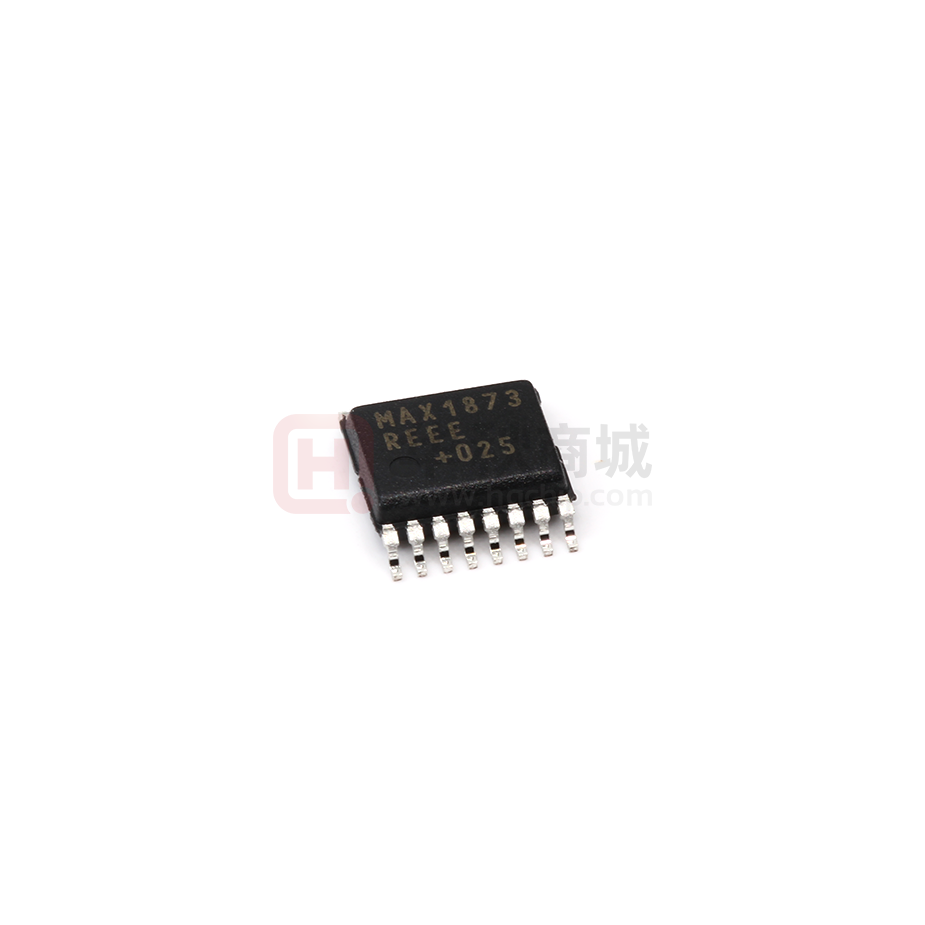
available in a space-saving 16-pin QSOP package. Use
the evaluation kit (MAX1873EVKIT) to help reduce
design time.
Applications
Features
o Low-Cost and Simple Circuit
o Charges 2-, 3-, or 4-Series Lithium-Ion Cells
o AC Adapter Input-Current-Limit Loop
o Also Charges Ni-Based Batteries
o Analog Output Monitors Charge Current
o ±0.75% Battery-Regulation Voltage
o 5µA Shutdown Battery Current
o Input Voltage Up to 28V
o 200mV Dropout Voltage/100% Duty Cycle
o Adjustable Charging Current
o 300kHz PWM Oscillator Reduces Noise
o Space-Saving 16-Pin QSOP
o MAX1873 Evaluation Kit Available to Speed
Designs
Ordering Information
PART
TEMP. RANGE
PIN-PACKAGE
MAX1873REEE
-40°C to +85°C
16 QSOP
Notebook Computers
MAX1873SEEE
-40°C to +85°C
16 QSOP
Portable Internet Tablets
MAX1873TEEE
-40°C to +85°C
16 QSOP
2-, 3-, or 4-cell Li+ Battery Pack Chargers
Typical Operating Circuit
6-, 9-, or 10-cell Ni Battery Pack Chargers
Hand-Held Instruments
Portable Desktop Assistants (PDAs)
Desktop Cradle Chargers
SYSTEM
LOAD
VIN 9V TO
28V
(9V MIN
FOR 2CELLS)
VH VL
Selector Guide
DCIN
CSSP
MAX1873
CSSN
PART
SERIES CELLS TO CHARGE
4V OUT PER
200mV ON RCS
MAX1873REEE
2-Cell Li+ or 5- or 6-cell Ni Battery
MAX1873SEEE
3-Cell Li+ or 7- or 9-cell Ni Battery
ICHG/EN
MAX1873TEEE
4-Cell Li+ 10-cell Ni Battery Packs
REF
IOUT
EXT
CSB
BATT
CCI
VADJ
Pin Configuration appears at end of data sheet.
CCS
GND
CCV
2- TO 4-CELL
Li+
________________________________________________________________ Maxim Integrated Products
For pricing, delivery, and ordering information, please contact Maxim/Dallas Direct! at
1-888-629-4642, or visit Maxim’s website at www.maxim-ic.com.
1
MAX1873
General Description
�MAX1873
Simple Current-Limited Switch-Mode
Li+ Charger Controller
ABSOLUTE MAXIMUM RATINGS
CSSP, CSSN, DCIN to GND ...................................-0.3V to +30V
VL, ICHG/EN to GND................................................-0.3V to +6V
VH, EXT to DCIN.......................................................-6V to +0.3V
VH, EXT to GND ......................................(VDCIN + 0.3V) to -0.3V
EXT to VH .................................................................+6V to -0.3V
DCIN to VL..............................................................+30V to -0.3V
VADJ, REF, CCI, CCV, CCS,
IOUT to GND.............................................-0.3V to (VL + 0.3V)
BATT, CSB to GND.................................................-0.3V to +20V
CSSP to CSSN.......................................................-0.3V to +0.6V
CSB to BATT..........................................................-0.3V to +0.6V
VL Source Current ............................................................+50mA
VH Sink Current ................................................................+40mA
Continuous Power Dissipation (TA = +70°C)
16-Pin QSOP (derate 8.3mW/°C above +70°C..........+667mW
Operating Temperature Range
MAX1873_EEE ................................................-40°C to +85°C
Junction Temperature ..................................................... +150°C
Storage Temperature Range .............................-65°C to +150°C
Lead Temperature (soldering, 10s) ................................ +300°C
Stresses beyond those listed under “Absolute Maximum Ratings” may cause permanent damage to the device. These are stress ratings only, and functional
operation of the device at these or any other conditions beyond those indicated in the operational sections of the specifications is not implied. Exposure to
absolute maximum rating conditions for extended periods may affect device reliability.
ELECTRICAL CHARACTERISTICS
(Circuit of Figure 1, VDCIN = VCSSP = VCSSN = 18V, VICHG/EN = VREF, VVADJ = VREF/2. MAX1873R: VBATT = VCSB = 8.4V;
MAX1873S: VBATT = VCSB = 12.6V; MAX1873T: VBATT = VCSB = 16.8V; TA = 0°C to +85°C. Typical values are at TA = +25°C, unless
otherwise noted.)
PARAMETER
CONDITIONS
MIN
TYP
MAX
UNITS
INPUT SUPPLY AND REFERENCE
DCIN Input Voltage Range
DCIN Quiescent Supply Current
6
6.0V < VDCIN < 28V
DCIN ≤ BATT
28
V
4
7
mA
0.1
10
µA
DCIN to BATT Undervoltage Threshold
CSSP = DCIN, input falling
0.05
0.175
V
DCIN to BATT Undervoltage Threshold
CSSP = DCIN, input rising
0.22
0.38
V
VL Output Voltage
6.0V < VDCIN < 28V
5.15
5.40
5.65
V
VL Output Load Regulation
IVL = 0 to 3mA
15
50
mV
REF Output Voltage
IREF = 21µA (200kΩ load)
4.179
4.20
4.221
V
2
6
mV
22
65
ppm/V
6
13
mV
300
330
kHz
4
7
Ω
2.5
4.5
Ω
REF Line Regulation
6.0V < VDCIN < 28V
REF Load Regulation
IREF = 0 to 1mA
SWITCHING REGULATOR
PWM Oscillator Frequency
270
EXT Driver Source On-Resistance
EXT Driver Sink On-Resistance
VH Output Voltage
DCIN - VH, 6V < VDCIN
很抱歉,暂时无法提供与“MAX1873REEE+T”相匹配的价格&库存,您可以联系我们找货
免费人工找货