19-2661; Rev 1; 9/05
Quick-PWM Step-Down Controllers with Inductor
Saturation Protection and Dynamic Output Voltages
♦
♦
♦
♦
♦
♦
♦
♦
♦
Inductor Saturation Protection
Accurate Current Limit
Ultra-High Efficiency
Quick-PWM with 100ns Load-Step Response
MAX1992
1.8V/2.5V Fixed or 0.7V to 5.5V Adjustable
Output Range
MAX1993
External Reference Input
Dynamically Selectable Output Voltage
(0.7V to 5.5V)
Optional Power-Good and Fault Blanking
During Transitions
±1% VOUT Accuracy Over Line and Load
2V to 28V Battery Input Range (VIN)
200/300/450/600kHz Switching Frequency
Overvoltage/Undervoltage Protection Option
1.7ms Digital Soft-Start
Drives Large Synchronous Rectifier FETs
2V ±0.7% Reference Output
Power-Good Window Comparator
Ordering Information
TEMP RANGE
PIN-PACKAGE
MAX1992ETG
PART
-40°C to +85°C
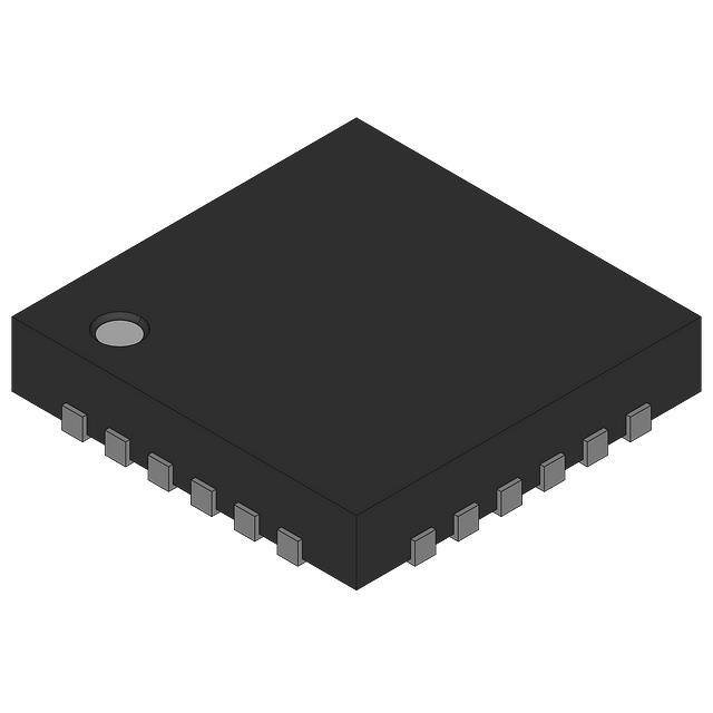
24 Thin QFN 4mm × 4mm
MAX1992ETG+
-40°C to +85°C
24 Thin QFN 4mm × 4mm
MAX1993ETG
-40°C to +85°C
24 Thin QFN 4mm × 4mm
MAX1993ETG+
-40°C to +85°C
24 Thin QFN 4mm × 4mm
+ Denotes lead-free package.
Pin Configurations
Active Termination Buses (MAX1993)
CPU/Chipset/GPU with Dynamic Voltage Cores
(MAX1993)
BST
LX
DH
V+
SKIP
15
14
13
12
CSN
PGND
20
11
CSP
AGND
21
VCC
22
MAX1992
10
OUT
9
FB
SHDN
23
8
N.C.
OVP/UVP
24
7
N.C
1
2
3
4
5
6
REF
DDR Memory Termination (MAX1993)
16
ILIM
1.8V and 2.5V Supplies
17
19
N.C.
Core/IO Supplies as Low as 0.7V
18
VDD
TON
Notebook Computers
DL
TOP VIEW
Applications
PGOOD
Single-stage buck conversion allows the MAX1992/
MAX1993 to directly step down high-voltage batteries for
the highest possible efficiency. Alternatively, two-stage
conversion (stepping down from another system supply
rail instead of the battery) at the maximum switching frequency allows the minimum possible physical size.
The MAX1992 powers the CPU core, chipset, DRAM, or
other supply rails as low as 0.7V. The MAX1993 powers
chipsets and graphics processor cores, which require
dynamically adjustable output voltages. The MAX1993
provides a tracking input that can be used for active termination buses. The MAX1992/MAX1993 are available in
a 24-pin thin QFN package with optional overvoltage and
undervoltage protection.
For dual step-down PWM controllers with inductor saturation protection, external reference input voltage, and
dynamically selectable output voltages, refer to the
MAX1540/MAX1541 data sheet.
♦
♦
♦
♦
♦
LSAT
The MAX1992/MAX1993 pulse-width modulation (PWM)
controllers provide high-efficiency, excellent transient
response, and high DC output accuracy. The devices
step down high-voltage batteries to generate lowvoltage CPU core or chipset/RAM supplies in notebook
computers.
Maxim’s proprietary Quick-PWM™ quick-response, constant on-time PWM control scheme handles wide
input/output voltage ratios with ease and provides 100ns
“instant-on” response to load transients, while maintaining
a relatively constant switching frequency. Efficiency is
enhanced by the ability to drive very large synchronousrectifier MOSFETs. Current sensing to ensure reliable
overload and inductor saturation protection is available
using an external current-sense resistor in series with the
output. Alternatively, the controller can sense the current
across the synchronous rectifier alone or use lossless
inductor sensing for lowest power dissipation.
Features
THIN QFN
4mm x 4mm
A "+" SIGN WILL REPLACE THE FIRST PIN INDICATOR ON LEAD-FREE PACKAGES.
Quick-PWM is a trademark of Maxim Integrated Products, Inc.
Pin Configurations continued at end of data sheet.
________________________________________________________________ Maxim Integrated Products
For pricing, delivery, and ordering information, please contact Maxim/Dallas Direct! at
1-888-629-4642, or visit Maxim’s website at www.maxim-ic.com.
1
MAX1992/MAX1993
General Description
�MAX1992/MAX1993
Quick-PWM Step-Down Controllers with Inductor
Saturation Protection and Dynamic Output Voltages
ABSOLUTE MAXIMUM RATINGS (Note 1)
V+ to AGND............................................................-0.3V to +30V
VCC to AGND............................................................-0.3V to +6V
VDD to PGND............................................................-0.3V to +6V
PGOOD, ILIM, SKIP, SHDN to AGND ......................-0.3V to +6V
REFIN, FB, CSP to AGND.........................................-0.3V to +6V
GATE, OD to GND (MAX1993 only) .........................-0.3V to +6V
TON, OVP/UVP, LSAT to AGND .................-0.3V to (VCC + 0.3V)
REF, OUT to AGND ....................................-0.3V to (VCC + 0.3V)
FBLANK to GND (MAX1993 only) ..............-0.3V to (VCC + 0.3V)
DL to PGND................................................-0.3V to (VDD + 0.3V)
CSN to AGND............................................................-2V to +30V
DH to LX .....................................................-0.3V to (BST + 0.3V)
LX to AGND ...............................................................-2V to +30V
BST to LX..................................................................-0.3V to +6V
AGND to PGND (MAX1992 only) ..........................-0.3V to +0.3V
REF Short Circuit to AGND.........................................Continuous
Continuous Power Dissipation (TA = +70°C)
24-Pin 4mm x 4mm Thin QFN
(derated 20.8mW/°C above +70°C)...........................1667mW
Operating Temperature Range
MAX199_ETG ..................................................-40°C to +85°C
Junction Temperature ......................................................+150°C
Storage Temperature Range .............................-65°C to +150°C
Lead Temperature (soldering, 10s) .................................+300°C
Note 1: For the MAX1993, AGND and PGND refer to a single pin designated GND.
Stresses beyond those listed under “Absolute Maximum Ratings” may cause permanent damage to the device. These are stress ratings only, and functional
operation of the device at these or any other conditions beyond those indicated in the operational sections of the specifications is not implied. Exposure to
absolute maximum rating conditions for extended periods may affect device reliability.
ELECTRICAL CHARACTERISTICS
(V+ = 15V, VCC = VDD = SHDN = 5V, SKIP = GND, TA = 0°C to +85°C, unless otherwise noted. Typical values are at TA = +25°C.)
PARAMETER
SYMBOL
CONDITIONS
MIN
TYP
MAX
UNITS
PWM CONTROLLER
Input Voltage Range
Output Voltage Accuracy
(MAX1992 Fixed)
Feedback Voltage Accuracy
(MAX1992 Adjustable)
Feedback Voltage Accuracy
(MAX1993)
VIN
VBIAS
VCC, VDD
VOUT
MAX1992
V+ = 4.5V to 28V,
SKIP = VCC
(Note 2)
FB = VCC
1.782
1.8
1.818
0.693
0.7
0.707
REFIN = 0.35 × REF
0.693
0.7
0.707
REFIN = REF
1.980
2
2.020
VFB
MAX1993
V+ = 4.5V to 28V,
SKIP = VCC
(Note 2)
0.1
VCC = 4.5V to 5.5V, V+ = 4.5V to 28V
IFB
MAX1992
%
0.25
%
-0.1
+0.1
µA
0.7
5.5
V
FB = GND
90
190
FB = VCC or adjustable
70
145
270
400
800
1400
10
25
Ω
0.3
0.4
V
RDISCHARGE
0.2
tSS
V
V
ILOAD = 0 to 3A, SKIP = VCC
ROUT
V
V
OUT Synchronous Rectifier
Discharge Mode Turn-On Level
2
5.5
2.525
MAX1993
Soft-Start Ramp Time
4.5
2.5
Output Adjust Range
OUT Discharge Mode
On-Resistance
28
2.475
MAX1992 V+ = 4.5V to 28V, SKIP = VCC
(Note 2)
Line Regulation Error
OUT Input Resistance
2
FB = GND
VFB
Load Regulation Error
FB Input Bias Current
Battery voltage, V+
Rising edge on SHDN to full current limit
1.7
_______________________________________________________________________________________
350
kΩ
ms
�Quick-PWM Step-Down Controllers with Inductor
Saturation Protection and Dynamic Output Voltages
MAX1992/MAX1993
ELECTRICAL CHARACTERISTICS (continued)
(V+ = 15V, VCC = VDD = SHDN = 5V, SKIP = GND, TA = 0°C to +85°C, unless otherwise noted. Typical values are at TA = +25°C.)
PARAMETER
SYMBOL
CONDITIONS
TON = GND (600kHz)
On-Time
tON
Minimum Off-Time
tOFF(MIN)
Quiescent Supply Current (VCC)
ICC
Quiescent Supply Current (VDD)
IDD
Quiescent Supply Current (V+)
IV+
V+ = 15V,
VOUT = 1.5V
(Note 3)
MIN
TYP
MAX
170
194
219
TON = REF (450kHz)
213
243
273
TON = open (300kHz)
316
352
389
TON = VCC (200kHz)
461
516
571
(Note 3)
400
500
FB forced above the regulation point,
LSAT = GND
0.55
0.85
UNITS
ns
ns
mA
FB forced above the regulation point,
VLSAT > 0.5V
1
20V) AC adapters. Low-current applications usually require less attention.
The high-side MOSFET (NH) must be able to dissipate
the resistive losses plus the switching losses at both
VIN(MIN) and VIN(MAX). Ideally, the losses at VIN(MIN)
should be roughly equal to the losses at VIN(MAX), with
lower losses in between. If the losses at VIN(MIN) are
significantly higher, consider increasing the size of NH.
Conversely, if the losses at VIN(MAX) are significantly
higher, consider reducing the size of NH. If VIN does
not vary over a wide range, maximum efficiency is
achieved by selecting a high-side MOSFET (N H) that
has conduction losses equal to the switching losses.
30
Choose a low-side MOSFET (NL) that has the lowest
possible on-resistance (RDS(ON)), comes in a moderatesized package (i.e., 8-pin SO, DPAK, or D2PAK), and is
reasonably priced. Ensure that the MAX1992/MAX1993
DL gate driver can supply sufficient current to support the
gate charge and the current injected into the parasitic
drain-to-gate capacitor caused by the high-side MOSFET
turning on; otherwise, cross-conduction problems can
occur. Switching losses are not an issue for the low-side
MOSFET since it is a zero-voltage switched device when
used in the step-down topology.
Power MOSFET Dissipation
Worst-case conduction losses occur at the duty factor
extremes. For the high-side MOSFET (NH), the worstcase power dissipation due to resistance occurs at
minimum input voltage:
⎛V
⎞
2
PD(NH Re sistive) = ⎜ OUT ⎟ (ILOAD ) RDS(ON)
⎝ VIN ⎠
Generally, use a small high-side MOSFET to reduce
switching losses at high-input voltages. However, the
RDS(ON) required to stay within package power-dissipation limits often limits how small the MOSFET can be.
The optimum efficiency occurs when the switching
losses equal the conduction (RDS(ON)) losses. Highside switching losses do not become an issue until the
input is greater than approximately 15V.
Calculating the power dissipation in high-side
MOSFETs (NH) due to switching losses is difficult, since
it must allow for difficult-to-quantify factors that influence the turn-on and turn-off times. These factors
include the internal gate resistance, gate charge,
threshold voltage, source inductance, and PC board
layout characteristics. The following switching loss calculation provides only a very rough estimate and is no
substitute for breadboard evaluation, preferably including verification using a thermocouple mounted on NH:
PD(NH
(VIN(MAX) )
Switching) =
2
CRSSfSW ILOAD
IGATE
where CRSS is the reverse transfer capacitance of NH,
and IGATE is the peak gate-drive source/sink current
(1A typ).
Switching losses in the high-side MOSFET can become
a heat problem when maximum AC adapter voltages
are applied, due to the squared term in the switchingloss equation (C x VIN2 x fSW).
______________________________________________________________________________________
�Quick-PWM Step-Down Controllers with Inductor
Saturation Protection and Dynamic Output Voltages
⎡ ⎛V
⎞⎤
2
PD(NL Re sistive) = ⎢1 − ⎜ OUT ⎟ ⎥(ILOAD ) RDS(ON)
V
⎢⎣ ⎝ IN ⎠ ⎥⎦
The absolute worst case for MOSFET power dissipation
occurs under heavy overload conditions that are
greater than ILOAD(MAX) but are not high enough to
exceed the current limit and cause the fault latch to trip.
To protect against this possibility, “overdesign” the circuit to tolerate:
⎛ ILOAD(MAX)LIR ⎞
ILOAD = IVALLEY(MAX) + ⎜
⎟
2
⎝
⎠
where I VALLEY(MAX) is the maximum valley current
allowed by the current-limit circuit, including threshold
tolerance and sense-resistance variation. The
MOSFETs must have a relatively large heatsink to handle the overload power dissipation.
Choose a Schottky diode (DL) with a forward voltage
drop low enough to prevent the low-side MOSFET’s
body diode from turning on during the dead time. As a
general rule, select a diode with a DC current rating
equal to 1/3 the load current. This diode is optional and
can be removed if efficiency is not critical.
Applications Information
Dropout Performance
The output voltage adjustable range for continuous-conduction operation is restricted by the nonadjustable minimum off-time one-shot. For best dropout performance,
use the slower (200kHz) on-time setting. When working
with low input voltages, the duty-factor limit must be calculated using worst-case values for on- and off-times.
Manufacturing tolerances and internal propagation
delays introduce an error to the TON K-factor. This error
is greater at higher frequencies (Table 3). Also, keep in
mind that transient response performance of buck regulators operated too close to dropout is poor, and bulk output capacitance must often be added (see the VSAG
equation in the Design Procedure section).
The absolute point of dropout is when the inductor current ramps down during the minimum off-time (ΔIDOWN)
as much as it ramps up during the on-time (ΔIUP). The
ratio h = ΔIUP/ΔIDOWN indicates the controller’s ability
to slew the inductor current higher in response to
increased load, and must always be greater than 1. As
h approaches 1, the absolute minimum dropout point,
the inductor current cannot increase as much during
each switching cycle, and V SAG greatly increases,
unless additional output capacitance is used.
A reasonable minimum value for h is 1.5, but adjusting
this up or down allows trade-offs between VSAG, output
capacitance, and minimum operating voltage. For a
given value of h, the minimum operating voltage can be
calculated as:
⎡
⎤
⎢
⎥
⎢ VOUT + VDROP1 ⎥
VIN(MIN) = ⎢
⎥ + VDROP2 − VDROP1
⎢ ⎛ h × t OFF(MIN) ⎞ ⎥
⎟⎥
⎢1 − ⎜
K
⎠⎦
⎣ ⎝
where VDROP1 and VDROP2 are the parasitic voltage
drops in the discharge and charge paths (see the OnTime One-Shot (TON) section), tOFF(MIN) is from the
Electrical Characteristics, and K is taken from Table 3.
The absolute minimum input voltage is calculated with h
= 1.
If the calculated VIN(MIN) is greater than the required
minimum input voltage, then operating frequency must
be reduced or output capacitance added to obtain an
acceptable VSAG. If operation near dropout is anticipated, calculate VSAG to be sure of adequate transient
response.
A dropout design example follows:
VOUT = 2.5V
fSW = 300kHz
K = 3.3µs, worst-case KMIN = 3.0µs
tOFF(MIN) = 500ns
VDROP1 = VDROP2 = 100mV
h = 1.5
⎡
⎤
⎢
⎥
2.5V + 0.1V ⎥
⎢
VIN(MIN) = ⎢
+ 0.1V − 0.1V = 3.47V
⎛
⎞⎥
⎢ 1 − ⎜ 1.5 × 500ns ⎟ ⎥
⎢⎣ ⎝ 3.0μs ⎠ ⎥⎦
______________________________________________________________________________________
31
MAX1992/MAX1993
If the high-side MOSFET chosen for adequate RDS(ON)
at low battery voltages becomes extraordinarily hot
when subjected to VIN(MAX), consider choosing another
MOSFET with lower parasitic capacitance.
For the low-side MOSFET (NL) the worst-case power
dissipation always occurs at maximum battery voltage:
�MAX1992/MAX1993
Quick-PWM Step-Down Controllers with Inductor
Saturation Protection and Dynamic Output Voltages
REF
R4
R1
REFIN
B
R3
C1
R2
MAX1993
A
GND
1kΩ
1000pF
GATE
1kΩ
1000pF
Figure 11. Multiple Output Voltage Settings
Calculating again with h = 1 and the typical K-factor
value (K = 3.3µs) gives the absolute limit of dropout:
⎡
⎤
⎢
⎥
2.5V + 0.1V ⎥
⎢
VIN(MIN) = ⎢
+ 0.1V − 0.1V = 3.06V
⎛
⎞⎥
⎢ 1 − ⎜ 1.5 × 500ns ⎟ ⎥
⎢⎣ ⎝ 3.3μs ⎠ ⎥⎦
Therefore, VIN must be greater than 3.06V, even with very
large output capacitance, and a practical input voltage
with reasonable output capacitance would be 3.47V.
Multiple Output Voltage Settings
(MAX1993 Only)
While the MAX1993 is optimized to work with applications that require two dynamic output voltages, it can
produce three or more output voltages if required by
using discrete logic or a DAC.
Figure 11 shows an application circuit providing four
voltage levels using discrete logic. Switching resistors
in and out of the resistor network changes the voltage
at REFIN. An edge detection circuit is added to generate a 1µs pulse on GATE to trigger the fault-blanking
and forced-PWM operation. When using PWM mode
(SKIP = V CC ), the edge detection circuit is only
required if fault blanking is enabled. Otherwise, leave
OD unconnected.
32
Active Bus Termination (MAX1993 Only)
Active bus termination power supplies generate a voltage rail that tracks a set reference. They are required to
source and sink current. DDR memory architecture
requires active bus termination. In DDR memory architecture, the termination voltage is set at exactly half the
memory supply voltage. Configure the MAX1993 to
generate the termination voltage using a resistordivider at REFIN. In such an application, the MAX1993
must be kept in PWM mode (SKIP = VCC) in order for it
to source and sink current. Figure 12 shows the
MAX1993 configured as a DDR termination regulator.
Connect GATE and FBLANK to GND when unused.
Voltage Positioning
In applications where fast-load transients occur, the
output voltage changes instantly by ESR COUT x
ΔILOAD. Voltage positioning allows the use of fewer output capacitors for such applications, and maximizes
the output voltage AC and DC tolerance window in tight
tolerance applications.
Figure 13 shows the connection of OUT and FB in a
voltage-positioned circuit. In nonvoltage-positioned circuits, the MAX1992/MAX1993 regulate at the output
capacitor. In voltage-positioned circuits, the MAX1992/
MAX1993 regulate on the inductor side of the currentsense resistor. VOUT is reduced to:
VOUT(VPS) = VOUT(NO LOAD) - RSENSEILOAD
______________________________________________________________________________________
�Quick-PWM Step-Down Controllers with Inductor
Saturation Protection and Dynamic Output Voltages
VCC
VIN
SKIP
DH
CIN
L
1000pF
REFIN
1000pF
RSENSE
V
VTT = DDQ
2
LX
10kΩ
COUT
DL
MAX1993 GND
10kΩ
CSP
OD
CSN
GATE
OUT
FBLANK
FB
VDDQ = DDR MEMORY SUPPLY VOLTAGE
VTT = TERMINATION SUPPLY VOLTAGE
Figure 12. Active Bus Termination
PC Board Layout Guidelines
Layout Procedure
Careful PC board layout is critical to achieve low
switching losses and clean, stable operation. The
switching power stage requires particular attention
(Figure 15). If possible, mount all of the power components on the topside of the board, with their ground terminals flush against one another. Follow these
guidelines for good PC board layout:
• Keep the high-current paths short, especially at the
ground terminals. This practice is essential for stable, jitter-free operation.
• Keep the power traces and load connections short.
This practice is essential for high efficiency. Using
thick copper PC boards (2oz vs. 1oz) can enhance
full-load efficiency by 1% or more. Correctly routing
PC board traces is a difficult task that must be
approached in terms of fractions of centimeters,
where a single milliohm of excess trace resistance
causes a measurable efficiency penalty.
• Minimize current-sensing errors by connecting CSP
and CSN directly across the current-sense resistor
(RSENSE).
• When trade-offs in trace lengths must be made, it is
preferable to allow the inductor-charging path to be
made longer than the discharge path. For example,
it is better to allow some extra distance between the
input capacitors and the high-side MOSFET than to
allow distance between the inductor and the lowside MOSFET or between the inductor and the output filter capacitor.
• Route high-speed switching nodes (BST, LX, DH,
and DL) away from sensitive analog areas (REF, FB,
CSP, and CSN).
1) Place the power components first, with ground terminals adjacent (N L source, C IN , C OUT , and D L
anode). If possible, make all these connections on
the top layer with wide, copper-filled areas.
2) Mount the controller IC adjacent to the low-side
MOSFET, preferably on the backside opposite NL
and NH in order to keep LX, GND, DH, and the DL
gate-drive lines short and wide. The DL and DH gate
traces must be short and wide (50 mils to 100 mils
wide if the MOSFET is 1in from the controller IC) to
keep the driver impedance low and for proper adaptive dead-time sensing.
3) Group the gate-drive components (BST diode and
capacitor, VDD bypass capacitor) together near the
controller IC.
4) Make the DC-DC controller ground connections as
shown in Figures 1 and 9. This diagram can be
viewed as having two separate ground planes:
power ground, where all the high-power components go; and an analog ground plane for sensitive
analog components. The analog ground plane and
power ground plane must meet only at a single point
directly at the IC.
5) Connect the output power planes directly to the output filter capacitor positive and negative terminals
with multiple vias. Place the entire DC-to-DC converter circuit as close to the load as is practical.
______________________________________________________________________________________
33
MAX1992/MAX1993
VDDQ
�MAX1992/MAX1993
Quick-PWM Step-Down Controllers with Inductor
Saturation Protection and Dynamic Output Voltages
R1
+5V BIAS
SUPPLY
C2
VDD
VCC
DBST
C1
V+
INPUT (VIN)
CIN
BST
NH
DH
CBST
MAX1992
L1
RSENSE
LX
NL
COUT
DL
DL
VOLTAGE-POSITIONED
OUTPUT (VOUT(VPS))
PGND
AGND
CSP
OUT
CSN
FB
VOUT(VPS) = VOUT(NO LOAD) - RSENSEIOUT
Figure 13. Voltage-Positioning Output
CAPACITIVE SOAR
(dV/dt = IOUT/COUT)
VOLTAGE POSITIONING THE OUTPUT
ESR VOLTAGE STEP
(ISTEP x RESR)
A
B
A. CONVENTIONAL CONVERTER
B. VOLTAGE-POSITIONED OUTPUT
VOUT
CAPACITIVE SAG
(dV/dt = IOUT/COUT)
RECOVERY
ILOAD
Figure 14. Voltage-Positioning Transient Response
34
______________________________________________________________________________________
�Quick-PWM Step-Down Controllers with Inductor
Saturation Protection and Dynamic Output Voltages
MAX1992/MAX1993
KELVIN SENSE VIAS UNDER
THE SENSE RESISTOR
(SEE EVALUATION KIT)
INDUCTOR
VIA TO POWER
GROUND
VIA TO ANALOG
GROUND
COUT
CONNECT GND
AND PGND TO THE
CONTROLLER AT
ONE POINT ONLY,
AS SHOWN
COUT
CIN
OUTPUT
INPUT
GROUND
CONNECT THE
EXPOSED PAD TO
ANALOG GND
MAX1992
Figure 15. PC Board Layout
LX
DH
V+
SKIP
14
13
BST
17
15
DL
18
TOP VIEW
16
Pin Configurations (continued)
VDD
19
12 CSN
GND
20
11 CSP
GATE
21
VCC
22
4
5
6
ILIM
REF
REFIN
PGOOD
7
3
OD
24
LSAT
23
2
FB
8
1
9
TON
OVP/UVP
10 OUT
MAX1993
FBLANK
SHDN
Chip Information
TRANSISTOR COUNT: 2616
PROCESS: BiCMOS
THIN QFN
4mm x 4mm
A "+" SIGN WILL REPLACE THE FIRST PIN INDICATOR ON LEAD-FREE PACKAGES.
______________________________________________________________________________________
35
�Package Information
(The package drawing(s) in this data sheet may not reflect the most current specifications. For the latest package outline information,
go to www.maxim-ic.com/packages.)
24L QFN THIN.EPS
MAX1992/MAX1993
Quick-PWM Step-Down Controllers with Inductor
Saturation Protection and Dynamic Output Voltages
PACKAGE OUTLINE,
12, 16, 20, 24, 28L THIN QFN, 4x4x0.8mm
21-0139
E
1
2
PACKAGE OUTLINE,
12, 16, 20, 24, 28L THIN QFN, 4x4x0.8mm
21-0139
E
2
2
Maxim cannot assume responsibility for use of any circuitry other than circuitry entirely embodied in a Maxim product. No circuit patent licenses are
implied. Maxim reserves the right to change the circuitry and specifications without notice at any time.
36 ____________________Maxim Integrated Products, 120 San Gabriel Drive, Sunnyvale, CA 94086 408-737-7600
© 2005 Maxim Integrated Products
Printed USA
is a registered trademark of Maxim Integrated Products, Inc.
�