EVALUATION KIT AVAILABLE
Click here for production status of specific part numbers.
MAX20096/MAX20097
Dual-Channel Synchronous Buck, High-Brightness
LED Controller with and without SPI Interface
General Description
The MAX20096/MAX20097 are dual-channel, highvoltage, synchronous n-channel high-current buck LED
drivers. The ICs use a proprietary average current-modecontrol scheme to regulate the inductor current. This
control method does not require any control-loop compensation, maintaining nearly constant switching frequency.
Inductor current sense is achieved by sensing the current
in the bottom switching device. The ICs integrate two fully
synchronous buck-converter controllers, and operate over
a wide 4.5V to 65V input range. The ICs are designed for
high-frequency operation and can operate at switching
frequencies as high as 1MHz.
In the MAX20096, the output voltages and currents on
both channels and the junction temperature can be read
back through the SPI interface. Protection features include
inductor current-limit protection, overvoltage protection,
and thermal shutdown. The MAX20096 is available in a
space-saving thermally enhanced (5mm x 5mm), 32-pin
side-wettable TQFN package and is specified to operate
over the -40°C to +125°C automotive temperature range.
The MAX20097 is available in a 28-pin thermally enhanced
TSSOP package, but does not have the SPI interface. It
includes an open-drain fault flag (FLTB) that goes low
in case of an open string, shorted string, or overvoltage
activation in any one of the channels, or also in thermal
shutdown.
Applications
● Automotive Exterior Lighting
• High-Beam/Low-Beam/Signal/Position Lights
• Daytime Running Lights (DRLs)
• Fog Light and Adaptive Front Light Assemblies
● Commercial, Industrial, and Architectural Lighting
19-100097; Rev 2; 2/19
Benefits and Features
● Integration Minimizes BOM for High-Brightness LED
Driver, Saving Space and Cost
• Wide 4.5V to 65V Input Voltage Range
• No Compensation Components
• Programmable Switching Frequency
• External MOSFETs that are Sizable for the
Appropriate Current
● Wide Dimming Ratio Allows High-Contrast Ratio
• Analog Dimming
• PWM Dimming
● Suitable for Matrix Lighting
• Maintains Current Regulation While Shorting/
Opening Individual LEDs in the String
• Ultra-Fast Response Control Loop Prevents
Overshoots and Undershoots
● Protection Features and Wide Temperature Range
Increase System Reliability
• Short Circuit, Overvoltage, and Thermal Protection
• -40ºC to +125ºC Operating Temperature Range
• Thermal Monitor and LED Current Monitor
● Fault Diagnosis Through SPI Interface and Through
FLTB Pin for Applications without SPI Interface
Ordering Information appears at end of data sheet.
�MAX20096/MAX20097
Dual-Channel Synchronous Buck, High-Brightness
LED Controller with and without SPI Interface
Absolute Maximum Ratings
VIN to VAGND.........................................................-0.3V to +70V
VLX_ to VAGND............................................-0.3V to (VIN + 0.3)V
VCSN_, VCSP_ to VAGND.........................................-2.5V to +6V
VCC, VIO to VAGND...............................................-0.3V to +6.0V
VBST_ to VAGND.................................................-0.3V to +72.0V
VBST_ to VLX_.......................................................-0.3V to +6.0V
VTON_ to VAGND....................................................-0.3V to +65V
VPGND to VAGND..................................................-0.3V to +0.3V
VREFI_ to VAGND..................................................-0.3V to +2.5V
VDIM_ to VAGND....................................................-0.3V to +6.0V
VOUT_, VCSB, VSCLK, VSDI, VRESETB to VAGND
-0.3V to +6.0V, VSDO to VAGND........... -0.3V to (VIO + 0.3)V
Short-Circuit Current on VCC.....................................Continuous
Continuous Power Dissipation (Multilayer Board)
32-Pin SW TQFN (TA = +70°C, derate 34.5mW/°C
above +70°C)..........................................................2758.6mW
Continuous Power Dissipation (Multilayer Board)
28-Pin TSSOP (TA = +70°C, derate 29.7mW/°C
above +70°C)................................................. mW to 2380mW
Operating Temperature Range.......................... -40°C to +125°C
Junction Temperature.......................................................+150°C
Storage Temperature Range............................. -40°C to +150°C
Soldering Temperature (reflow)........................................+260°C
Stresses beyond those listed under “Absolute Maximum Ratings” may cause permanent damage to the device. These are stress ratings only, and functional operation of the device at these
or any other conditions beyond those indicated in the operational sections of the specifications is not implied. Exposure to absolute maximum rating conditions for extended periods may affect
device reliability.
Package Thermal Characteristics (Note 1)
32-Pin SW TQFN
Thermal Resistance, Single-Layer Board:
Junction-to-Ambient Thermal Resistance (θJA)...........47°C/W
Junction-to-Case Thermal Resistance (θJC)..................3°C/W
28-Pin TSSOP
Thermal Resistance, Single-Layer Board:
Junction-to-Ambient Thermal Resistance (θJA)...........45°C/W
Junction-to-Case Thermal Resistance (θJC)..................2°C/W
Thermal Resistance, Four-Layer Board:
Junction-to-Ambient Thermal Resistance (θJA)...........36°C/W
Junction-to-Case Thermal Resistance (θJC)..................3°C/W
Thermal Resistance, Four-Layer Board:
Junction-to-Ambient Thermal Resistance (θJA)........33.6°C/W
Junction-to-Case Thermal Resistance (θJC)...............3.3°C/W
Note 1: Package thermal resistances were obtained using the method described in JEDEC specification JESD51-7, using a four-layer
board. For detailed information on package thermal considerations, refer to www.maximintegrated.com/thermal-tutorial.
For the latest package outline information and land patterns (footprints), go to www.maximintegrated.com/packages. Note
that a “+”, “#”, or “-” in the package code indicates RoHS status only. Package drawings may show a different suffix character,
but the drawing pertains to the package regardless of RoHS status.
Electrical Characteristics
(VIN = 12V, Limits are 100% tested at TA = +25°C and TA = +125°C. Limits over the operating temperature range and relevant supply
voltage range are guaranteed by design and characterization. Specifications marked “GBD” are guaranteed by design and not production
tested.)
PARAMETER
SYMBOL
CONDITIONS
MIN
TYP
MAX
UNITS
INPUT SUPPLY VOLTAGE
Operational Supply Voltage
VIN
IN Supply Current
IINQ
4.5
DIM1 = DIM2 = 5V
65
V
10
mA
V
V CC REGULATOR
Output Voltage
VCC
VCC Dropout Voltage
IVCC = 1mA, 5.5V < VIN < 65V
4.875
5.0
5.125
IVCC = 10mA, 6V < VIN < 25V
4.875
5.0
5.125
500
IVCC = 10mA, VIN1 = 4.5V
200
VCCIMAX
VCC = 0V
60
VCC Undervoltage Lockout,
Rising
VCCUVLOR
INS rising
3.8
4.1
4.4
V
VCC Undervoltage Lockout,
Falling
VCCUVLOF
INS falling
3.55
3.85
4.15
V
VCC Short-Circuit Current
www.maximintegrated.com
mV
mA
Maxim Integrated │ 2
�MAX20096/MAX20097
Dual-Channel Synchronous Buck, High-Brightness
LED Controller with and without SPI Interface
Electrical Characteristics (continued)
(VIN = 12V, Limits are 100% tested at TA = +25°C and TA = +125°C. Limits over the operating temperature range and relevant supply
voltage range are guaranteed by design and characterization. Specifications marked “GBD” are guaranteed by design and not production
tested.)
PARAMETER
SYMBOL
CONDITIONS
MIN
TYP
MAX
UNITS
1.2
V
0.195
V
ANALOG DIMMING INPUT
REFI Input Voltage Range
(Fail-Safe Mode)
REFI Zero-Current Threshold,
Falling (Fail-Safe Mode)
REFIRNG
RESETB = 0 or RESETB = 1 with CNFG_
SEL = 0
0.2
REFIZC_TH
RESETB = 0 or RESETB = 1 with CNFG_
SEL = 0, CS < 5mV
0.165
Zero-Current Threshold, Falling
(SPI Enabled)
REFI Clamp Voltage
REFI Input Bias Current
0.18
0.176
A
REFICLMP
RESETB = 0 or RESETB = 1 with CNFG_
SEL = 0, IREFI sink = 1μA
1.274
1.3
1.326
V
REFIIN
RESETB = 0 or RESETB = 1 with CNFG_
SEL = 0
0
20
200
nA
60
100
ns
ON-TIME CONTROL/OVERVOLTAGE PROTECTION/SHORT FAULT INDICATOR
Minimum On-Time
Programmed On-Time
tON-MIN
tON
VOUT_= 1V, C1 = C4 = 1nF, R1 = R4 =
24.9kΩ, VIN = 12V
2.27
TON_ Pulldown Resistance
OUT_ Overvoltage Threshold
VTH_OVP_
OUT_ Overvoltage Hysteresis
Short Fault Threshold
OUT rising, RESETB = 0 or RESETB = 1
and SPI_EN = 0
2.45
μs
15
40
Ω
2.5
2.55
V
OUT_ falling
22
Output failing, VOUT_ is lower than
threshold, no SPI
50
SPI enabled, V_SHORT_[1:0] = b’00,
VOUT_ is lower than threshold
100
SPI enabled, V_SHORT_[1:0] = 11,
VOUT_is lower than threshold
400
VCS_ = 0V
160
mV
mV
OFF-TIME CONTROL
Minimum Off-Time
Linear Range of Pulse Doubler
0.25
Maximum Off-Time
280
ns
2.5
μs
42
μs
PWM DIMMING (FAIL-SAFE MODE)
Internal Ramp Frequency
fRAMP
Phase Shift Between DIM1 and
DIM2
PSFT
External Sync Frequency
Range
Fail-safe mode using internal 200Hz
dimming
VLTH
External Sync High-Level
Voltage
VHTH
200
220
180
80
External Sync Low-Level
Voltage
www.maximintegrated.com
180
Hz
deg
2000
Hz
V
0.4
3.2
V
Maxim Integrated │ 3
�MAX20096/MAX20097
Dual-Channel Synchronous Buck, High-Brightness
LED Controller with and without SPI Interface
Electrical Characteristics (continued)
(VIN = 12V, Limits are 100% tested at TA = +25°C and TA = +125°C. Limits over the operating temperature range and relevant supply
voltage range are guaranteed by design and characterization. Specifications marked “GBD” are guaranteed by design and not production
tested.)
MIN
TYP
MAX
UNITS
DIM Comparator Offset Voltage
PARAMETER
SYMBOL
CONDITIONS
170
200
230
mV
DIM Voltage for 100% Duty
Cycle
3.2
V
PWM DIMMING (SPI CONTROLLED)
Programmed Dimming
Frequency
Programmed DIM Duty Cycle
SPI enabled with PWM1_SEL = PWM2_
SEL = 1, PWM_FREQ[2:0] = 0
200
SPI enabled with PWM1_SEL = PWM2_
SEL = 1, PWM_FREQ[2:0] = 110
2000
SPI enabled with PWM1_SEL = PWM2_
SEL = 1, PWM_FREQ[2:0] = 001
333
SPI is enabled, PWM1_SEL = PWM2_SEL
= 1, PWM_DUTY[9:0] = 1LSB
0.1
SPI is enabled, PWM1_SEL = PWM2_SEL
= 1, PWM_DUTY[9:0] = 500
50
SPI is enabled, PWM1_SEL = PWM2_SEL
= 1, PWM_DUTY[9:0] = 1000
100
Hz
%
CURRENT-SENSE AMPLIFIER
Current-Sense Amplifier Offset
0.192
0.2
0.208
V
Current-Sense Gain
4.84
5.0
5.12
V/V
CURRENT MONITOR
Offset Voltage
Current Monitor Amplifier Gain
0.2
V
5
V/V
DH_ AND DL_ DRIVERS
DH_ Sourcing Resistance
RON_HS
DH_ = high, TA = -40°C to +125°C
2.5
5.0
Ω
DH_ Sinking Resistance
RDH_SINK
DH_= low, TA = -40°C to 125°C
1.0
2.0
Ω
DL_ Sourcing Resistance
RDL_SRC
DL_ = high, TA = -40°C to +125°C
2.5
5.0
Ω
DL_ Sinking Resistance
RDL_SINK
DL _= low, TA = -40°C to +125°C
1.8
3.5
Ω
DH_-to-DL_ Dead Time
DH_ fall to DL_ rise, CL = 1nF (measured at
VTH = 1.5V)
20
ns
DL_-to-DH_ Dead Time
DL_ fall to DH_ rise, CL = 1nF (measured at
VTH = 1.5V)
20
ns
8
bits
ADC (MAX20096 ONLY)
Resolution
Offset Error
-2
+2
%FS
Gain Error
-2
+2
%FS
1.8
5.5
V
1
μA
SPI ELECTRICAL CHARACTERISTICS (MAX20096 ONLY)
I/O Supply Voltage
Static I/O Supply Current
(Note 2)
www.maximintegrated.com
VIO
IDDIO
Static inputs, all outputs unloaded
Maxim Integrated │ 4
�MAX20096/MAX20097
Dual-Channel Synchronous Buck, High-Brightness
LED Controller with and without SPI Interface
Electrical Characteristics (continued)
(VIN = 12V, Limits are 100% tested at TA = +25°C and TA = +125°C. Limits over the operating temperature range and relevant supply
voltage range are guaranteed by design and characterization. Specifications marked “GBD” are guaranteed by design and not production
tested.)
PARAMETER
SYMBOL
CONDITIONS
MIN
TYP
MAX
UNITS
DIGITAL INPUT CHARACTERISTICS (SCLK, SDI, CSB, RESETB)
Input High-Voltage VMAX
VIH
2.2V < VIO < 5.5V
0.7 x
VIO
V
Input High-Voltage VMIN
VIH
1.8V < VIO < 2.2V
0.8 x
VIO
V
Input Low-Voltage VMAX
VIL
2.2V < VIO < 5.5V
0.3 x
VIO
V
Input Low-Voltage VMIN
VIL
1.8V < VIO < 2.2V
0.2 x
VIO
V
Input Leakage Current (Note 3)
IIN
VIN = 0V or VIO
±0.1
±1
μA
Internal Safety-Impedance
Pulldown (Notes 4, 5)
RPD
SDI, SCLK pulldown to AGND
40
100
160
kΩ
Internal Safety-Impedance
Pullup (Notes 4, 5)
RPU
CSB, RESETB pullup to VIO
40
100
160
kΩ
Input Capacitance
CIN
10
pF
Hysteresis Voltage
VH
0.35
V
DIGITAL OUTPUT CHARACTERISTICS (SDO)
Output High-Voltage VMAX
VOH
VIO > 2.5V, ISOURCE = 5mA
VIO
-0.4
V
Output High-Voltage VMIN
VOH
VIO > 1.8V, ISOURCE = 2mA
VIO
-0.4
V
Output Low-Voltage VMAX
VOL
VIO > 2.5V, ISINK = 5mA
Output Low-Voltage VMIN
VOL
VIO > 1.8V, ISINK = 2mA
Output Short-Circuit Current
IOSS
ISINK, ISOURCE
Output Three-State Leakage
IOZ
±0.1
COZ
10
Output Three-State
Capacitance
0.4
0.4
250
V
V
mA
±1
µA
pF
SPI TIMING CHARACTERISTICS (MAX20096 ONLY)
SCLK Frequency
fSCLK
0
SCLK Period
tCP
250
SCLK Pulse Width High
tCH
SCLK Pulse Width Low
tCL
CSB Fall to SCLK Rise
Setup Time
tCSS0
To 1st SCLK rising edge (RE) (Note 6)
25
ns
CSB Fall to SCLK Rise Hold
Time
tCSH0
Applies to inactive rising edge preceding 1st
rising edge
25
ns
CSB Rise to SCLK Rise Hold
Time
tCSH1
Applies to N x 16th rising edge
25
ns
www.maximintegrated.com
(Note 6)
4
MHz
ns
62.5
ns
62.5
ns
Maxim Integrated │ 5
�MAX20096/MAX20097
Dual-Channel Synchronous Buck, High-Brightness
LED Controller with and without SPI Interface
Electrical Characteristics (continued)
(VIN = 12V, Limits are 100% tested at TA = +25°C and TA = +125°C. Limits over the operating temperature range and relevant supply
voltage range are guaranteed by design and characterization. Specifications marked “GBD” are guaranteed by design and not production
tested.)
PARAMETER
SYMBOL
CONDITIONS
MIN
CSB Rise to SCLK Rise
tCSA
Applies to N x 16th rising edge, guarantees
aborted (unqualified) sequence
25
ns
CSB Rise to SCLK Rise
tCSQ
Applies to (N x 16) + 1 rising edge,
guarantees qualified sequence
25
ns
tCSPW
100
ns
SDI-to-SCLK Rise Setup Time
tDS
20
ns
SDI-to-SCLK Rise Hold Time
tDH
20
ns
CSB Pulse Width High
TYP
MAX
UNITS
RESETB Pulse Width Low
tRBPW
For request to be recognized
25
ns
RESETB Rise to CSB Fall
Removal
tRBCS
For write transaction to be executed
20
ns
SCLK Fall to SDO Transition
tDOT
CLOAD = 20pF
100
SCLK Fall to SDO Hold
tDOH
CLOAD = 0pF
CSB Fall to SDO Transition
tDOE
CLOAD = 20pF
100
ns
CSB Rise to SDO Hi-Z
tDOZ
Output disable time
80
ns
2
ns
ns
THERMAL SHUTDOWN
Thermal Warning
(MAX20096 only)
150
ºC
Thermal Shutdown
165
ºC
Hysteresis
15
ºC
Note
Note
Note
Note
Note
2: Static logic inputs with VIL = AGND and VIH = VIO. CSB, RESETB = VIH (if safety pullup active).
3: No internal safety pullup/pulldown impedances active, input buffers only.
4: Internal safety pullup/pulldown impedances available, with enable function.
5: If pullup is supported, note CSB and RESETB connection and diode to VIO; this diode is present regardless of enable mode.
6: Applications must afford time for the device to drive data on the SDO bus and meet the µC setup time prior to the µC latching in the result on the following SCLK rising edge. In practice, this is determined by loading and µC characteristics, and the
relevant tDOT/tDOE specification must be satisfied.
www.maximintegrated.com
Maxim Integrated │ 6
�MAX20096/MAX20097
Dual-Channel Synchronous Buck, High-Brightness
LED Controller with and without SPI Interface
Typical Operating Characteristics
(TA = +25°C, unless otherwise noted.)
EFFICIENCY vs. LED CURRENT
% ERROR vs. ILED[6:0]
LED CURRENT vs. ILED[6:0]
toc01
100
3.0
8
90
6
60
50
40
30
2.0
1.5
0
1
2
LED CURRENT (A)
0.0
0
-6
ILED MEASURED (A)
ILED SETTING (A)
ILED ADC (A)
0
16
32
48
64
80
96
112
EFFICIENCY vs. LED CURRENT
-10
128
toc05
70
60
+25°C; 2 LEDs; 24VIN
-40°C; 2 LEDs; 24VIN
+85°C; 2 LEDs; 24VIN
80
96
112
128
toc06
4
2.0
1.5
1.0
0.0
VIN = 24V
0
16
32
48
64
80
96
ILED[6:0] DECIMAL)
2
0
-2
VIN = 24V
-4
ILED MEASURED (A)
ILED SETTING (A)
ILED ADC (A)
112
-6
% ERROR (SETTING)
% ERROR (ADC)
-8
-10
128
EFFICIENCY vs. LED CURRENT
0
16
32
48
64
80
ILED[6:0] (decimal)
LED CURRENT vs. ILED[6:0]
toc07
100
64
6
0.5
3
48
8
ERROR (%)
LED CURRENT (A)
EFFICIENCY (%)
80
1
2
LED CURRENT (A)
32
% ERROR vs. ILED[6:0]
10
2.5
0
16
LED CURRENT vs. ILED[6:0]
toc04
90
30
0
ILED[6:0] (decimal)
3.0
40
% ERROR (SETTING)
% ERROR (ADC)
-8
ILED[6:0] (decimal)
100
50
VIN = 14V
-4
VIN = 14V
0.5
3
2
-2
1.0
+25°C; 2 LED; 14V IN
-40°C; 2 LED; 14V IN
+85°C; 2 LED; 14V IN
4
ERROR (%)
LED CURRENT (A)
EFFICIENCY (%)
2.5
80
70
toc03
10
toc02
96
112
128
toc08
3.0
90
LED CURRENT (A)
EFFICIENCY (%)
2.5
80
70
60
50
+25°C; 2 LEDs; 36VIN
-40°C; 2 LEDs; 36VIN
+85°C; 2 LEDs; 36VIN
40
30
0
www.maximintegrated.com
1
2
LED CURRENT (A)
2.0
1.5
1.0
VIN = 36V
ILED MEASURED (A)
ILED SETTING (A)
ILED ADC (A)
0.5
3
0.0
0
16
32
48
64
80
ILED[6:0] (decimal)
96
112
128
Maxim Integrated │ 7
�MAX20096/MAX20097
Dual-Channel Synchronous Buck, High-Brightness
LED Controller with and without SPI Interface
Typical Operating Characteristics (continued)
(TA = +25°C, unless otherwise noted.)
% ERROR vs. ILED[6:0]
EFFICIENCY vs. LED CURRENT
toc09
10
100
LED CURRENT vs. ILED[6:0]
toc10
8
90
6
2.5
2
0
-2
VIN = 36V
-4
-6
70
60
0
16
32
+25°C; 2 LEDs; 48VIN
-40°C; 2 LEDs; 48VIN
+85°C; 2 LEDs; 48VIN
50
% ERROR (SETTING)
% ERROR (ADC)
-8
48
64
80
ILED[6:0] (decimal)
96
40
112
30
128
toc12
ILED MEASURED (A)
ILED SETTING (A)
ILED ADC (A)
0
16
32
48
64
80
ILED[6:0] (decimal)
96
LED CURRENT vs. ILED[6:0]
toc13
112
128
toc14
3.0
90
2.5
EFFICIENCY (%)
2
0
-2
-4
60
30
0
16
32
48
64
80
96
112
+25°C; 4 LEDs; 48VIN
-40°C; 4 LEDs; 48VIN
+85°C; 4 LEDs; 48VIN
40
% ERROR (SETTING)
% ERROR (ADC)
-8
70
50
VIN = 48V
-6
LED CURRENT (A)
80
4
ERROR (%)
VIN = 48V
1.0
3
6
-10
1.5
0.5
1
2
LED CURRENT (A)
100
8
2.0
0.0
0
EFFICIENCY vs. LED CURRENT
% ERROR vs. ILED[6:0]
10
LED CURRENT (A)
80
EFFICIENCY (%)
ERROR (%)
4
-10
toc11
3.0
128
ILED[6:0] (decimal)
0
1
2
LED CURRENT (A)
2.0
1.5
VIN = 48V
1.0
ILED MEASURED (A)
ILED SETTING (A)
ILED ADC (A)
0.5
0.0
3
0
16
32
48
64
80
96
112
128
ILED[6:0] (decimal)
EFFICIENCY vs. LED CURRENT
% ERROR vs. ILED[6:0]
toc15
10
toc16
100
8
90
6
EFFICIENCY (%)
ERROR (%)
4
2
0
-2
-4
VIN = 48V
-6
70
60
50
% ERROR (SETTING)
% ERROR (ADC)
-8
-10
80
30
0
16
32
48
64
80
ILED[6:0] (decimal)
www.maximintegrated.com
96
112
+25°C; 8 LEDs; 48VIN
-40°C; 8 LEDs; 48VIN
+85°C; 8 LEDs; 48VIN
40
128
0
1
2
3
LED CURRENT (A)
Maxim Integrated │ 8
�MAX20096/MAX20097
Dual-Channel Synchronous Buck, High-Brightness
LED Controller with and without SPI Interface
Typical Operating Characteristics (continued)
(TA = +25°C, unless otherwise noted.)
LED CURRENT vs. ILED[6:0]
% ERROR vs. ILED[6:0]
toc17
10
3.0
90
6
80
ERROR (%)
1.5
VIN = 48V
1.0
0.0
0
16
32
48
64
80
96
2
0
-2
-4
ILED MEASURED (A)
ILED SETTING (A)
ILED ADC (A)
0.5
DUTY CYCLE (%)
4
2.0
112
128
ILED[6:0] (decimal)
0
16
32
48
64
80
VCC SHORT-CIRCUIT CURRENT
vs. TEMPERATURE
96
112
DC (%)
0
256
512
768
1024
PWM_DUTY1[9:0] (decimal)
VCC vs. VIN
toc20
toc21
5.1
5.0
80
70
4.9
VCC (V)
SHORT-CIRCUIT CURRENT (mA)
40
0
128
90
60
50
40
4.8
4.7
30
VIN = 8V
20
4.6
TA = +25°C; 10mA LOAD
10
0
4.5
-40
-10
20
50
80
110
5
15
AMBIENT TEMPERATURE (°C)
VCC vs. TEMPERATURE
5.10
35
45
toc23
125
110
95
TEMPERATURE (°C)
5.06
5.04
5.02
5.00
4.98
80
65
50
35
20
4.96
5
4.94
-10
4.92
4.90
25
VIN (V)
TEMPERATURE vs. MON_TEMP[7:0]
toc22
5.08
VCC (V)
50
10
ILED[6:0] (decimal)
100
60
20
% ERROR (SETTING)
% ERROR (ADC)
-8
70
30
VIN = 48V
-6
-10
toc19
100
8
2.5
LED CURRENT (A)
DUTY CYCLE vs. PWM_DUTY1[9:0]
toc18
10mA LOAD, VIN = 14V
-40
-40
-10
20
50
80
AMBIENT TEMPERATURE (°C)
www.maximintegrated.com
CALCULATED (°C)
TC MEASURED (°C)
-25
110
100
120
140
160
180
200
MON_TEMP[7:0]
Maxim Integrated │ 9
�MAX20096/MAX20097
Dual-Channel Synchronous Buck, High-Brightness
LED Controller with and without SPI Interface
32
31
30
29
28
27
26
25
DL1
TON1
OUT1
CSP1
CSN1
REFI1
IOUTV1
DIM1
Pin Configurations
1 LX1
RESETB 24
SDO 23
2 BST1
3 DH1
VIO 22
4 IN
AGND 21
MAX20096
5 PGND
6 DH2
VCC 20
SDI 19
GND ON
BACKSIDE PAD
7 BST2
SCLK 18
8 LX2
IOUTV2
DIM2
11
REFI2
10
CSP2
OUT2
9
CSN2
DL2
TON2
CSB 17
12
13
14
15
16
TOP VIEW
+
OUT1
1
28
CSP1
TON1
2
27
CSN1
DL1
3
26
REFI1
LX1
4
25
IOUTV1
BST1
5
24
DIM1
DH1
6
23
FLTB
IN
7
22
VIO
PGND
8
21
AGND
DH2
9
20
VCC
BST2
10
19
DIM2
MAX20097
LX2
11
18
IOUTV2
DL2
12
17
REFI2
TON2
13
16
CSN2
OUT2
14
15
CSP2
EP
TSSOP
www.maximintegrated.com
Maxim Integrated │ 10
�MAX20096/MAX20097
Dual-Channel Synchronous Buck, High-Brightness
LED Controller with and without SPI Interface
Pin Description
PIN
SW TQFN
MAX20096
TSSOP
MAX20097
NAME
1
4
LX1
2
5
BST1
High-Side Power Supply for High-Side Gate Drive for Channel 1. Connect a 0.1μF
ceramic capacitor from BST1 to LX1.
3
6
DH1
High-Side Driver of Channel 1. Connect to gate of high-side n-channel MOSFET of
buck LED driver for channel 1. Use a series resistor to limit current slew rate and
mitigate EMI noise, if required.
4
7
IN
5
8
PGND
6
9
DH2
High-Side Driver of Channel 2. Connect to gate of high-side n-channel MOSFET of
buck LED driver for channel 2. Use a series resistor to limit current slew rate and
mitigate EMI noise, if required.
7
10
BST2
High-Side Power Supply for High-Side Gate Drive for Channel 2. Connect a 0.1μF
ceramic capacitor from BST2 to LX2.
8
11
LX2
Switching Node of Buck LED Driver on Channel 2. Connect to one end of output
inductor on channel 2.
9
12
DL2
Low-Side Driver of Channel 2. Connect to gate of low-side n-channel MOSFET of LED
driver for channel 2. Use a series resistor to limit current slew rate and mitigate EMI
noise, if necessary.
10
13
TON2
Frequency-Setting Pin for Channel 2. Connect a resistor to the input supply and
capacitor to AGND to set switching frequency for channel 2.
11
14
OUT2
Connect a resistor-divider from OUT2 to the output voltage on channel 2. OUT2 has the
scaled-down feedback of the output voltage on channel 2.
12
15
CSP2
Current-Sense Input on Channel 2. Connect to source of external MOSFET driven by
DL2. Connect a resistor from this pin to CSN2 to sense the current in the MOSFET.
13
16
CSN2
Negative Current-Sense Connection on Channel 2. Connect this pin to power ground.
14
17
REFI2
Analog Dimming Input for Channel 2 in Default Mode. Connect to a resistor-divider from
VCC to set the default LED current in channel 2.
15
18
IOUTV2
16
19
DIM2
PWM Dimming Input in Default Mode for Channel 2. Connect to an external PWM
signal or connect to an analog voltage between 0.2V and 3V to set the PWM duty cycle
in channel 2.
17
—
CSB
Chip-Select Pin for SPI Interface. This pin is pulled low to enable the SPI Interface.
18
—
SCLK
Clock Input Pin for SPI Interface
19
—
SDI
Data Input Pin for SPI Interface
20
20
VCC
+5V Regulator Output. Connect a 1µF ceramic capacitor from this pin to GND. If an
internal VCC regulator is not used, then connect VCC to IN and connect an external VCC
to this pin.
www.maximintegrated.com
FUNCTION
Switching Node of Buck LED Driver on Channel 1. Connect to one end of output
inductor on channel 1.
Supply Input Pin for VCC Regulator. Connect a 1µF ceramic capacitor from IN to PGND.
If an external VCC regulator is used, then connect IN to VCC.
Power-Ground Connection
Current Monitor Output on Channel 2
Maxim Integrated │ 11
�MAX20096/MAX20097
Dual-Channel Synchronous Buck, High-Brightness
LED Controller with and without SPI Interface
Pin Description (continued)
PIN
SW-TQFN
MAX20096
TSSOP
MAX20097
NAME
21
21
AGND
22
22
VIO
Microcontroller Power Supply Pin for MAX20096. For the MAX20097, connect VIO to
VCC externally
23
—
SDO
Data Output Pin for SPI Interface externally
24
—
RESETB
Active-Low Reset Pin for SPI. Toggling the reset pin switches control switches
programming of REFI_, DIM_, and oscillator frequency on both channels to the analog
control pins.
25
24
DIM1
PWM Dimming Input in Default Mode for Channel 1. Connect to an external PWM
signal or connect it to an analog voltage between 0.2V to 3V to set the PWM duty cycle
in Channel 1.
26
25
IOUTV1
27
26
REFI1
28
27
CSN1
29
28
CSP1
30
1
OUT1
31
2
TON1
32
3
DL1
Low-Side Driver of Channel 1. Connect to gate of low-side N-channel MOSFET of LED
Driver for channel 1. Use series resistor to limit current slew-rate and mitigate EMI noise
if necessary.
—
23
FLTB
Fault Flag Output in MAX20097
—
—
EP
www.maximintegrated.com
FUNCTION
Analog Ground Connection
Current Monitor Output on Channel 1
Analog Dimming Input for Channel 1 in Default Mode. Connect to a resistor divider from
VCC to set the default LED Current in Channel 1.
Negative Current-Sense Connection on Channel 1. Connect CSN1 to power ground.
Current-Sense Input on Channel 1. Connect to source of external MOSFET that is
driven by DL1. Connect a resistor from this pin to CSN1 to sense the current in the
MOSFET.
Connect a resistor divider from this pin to the output voltage on channel 1. This pin has
the scaled down feedback of the output voltage on channel 1.
Frequency-Setting Pin for Channel 1. Connect a resistor to the input supply and
capacitor to AGND to set switching frequency for channel 1.
Exposed Pad. Connect EP to a large-area contiguous copper ground plane for
effective power dissipation. Do not use as the main IC ground connection. EP must be
connected to GND.
Maxim Integrated │ 12
�MAX20096/MAX20097
Dual-Channel Synchronous Buck, High-Brightness
LED Controller with and without SPI Interface
Buck Diagrams
MAX20096
VIN
CIN
D1
VCC
R1
VCC
R7
CVCC
R8
BST1
IN
VCC
Q1
CBST1
DH1
TON1
C1
L1
LX1
Q2
DIM1
R9
IOUTV1
C3
R4
VCC
R11
R3
RCS1
MAX20096
R16
CSN1
RESET FROM EXTERNAL
WATCHDOG
VIN
R2
CSP1
DIM2
R10
COUT1
DL1
C4
R15
RESETB
TON2
OUT1
IOUTV2
BST2
C2
VIN
VCC
D2
Q3
DH2
R12
CBST2
REFI1
LX2
REFI2
R13
Q4
VIO
µC
COUT2
R5
DL2
CSB
R14
L2
SCLK
CSP2
R6
RCS2
SDI
CSN2
SDO
EP
www.maximintegrated.com
AGND
PGND
OUT2
Maxim Integrated │ 13
�MAX20096/MAX20097
Dual-Channel Synchronous Buck, High-Brightness
LED Controller with and without SPI Interface
Buck Diagrams (continued)
MAX20097
VIN
CIN
D1
VCC
R1
CVCC
C1
IN
TON1
REFI1
REFI1
R4
CBST1
L2
LX1
DIM1
R16
Q1
DH1
VIO
PWM1
CURRENT MONITOR ON
CHANNEL 1
BST1
VCC
COUT1
DL1
R2
Q2
CSP1
R3
MAX20097
RCS1
CSN1
IOUTV1
OUT1
C3
VCC
BST2
TON2
VIN
C2
PWM1
DIM2
REFI2
REFI2
FAULT
FLTB
DH2
LX2
Q3
CBST2
L2
COUT2
IOUTV2
CURRENT MONITOR ON
CHANNEL 2
R15
DL2
R5
Q4
C2
CSP2
R6
CSN2
PGND
www.maximintegrated.com
AGND
RCS2
OUT2
Maxim Integrated │ 14
�MAX20096/MAX20097
Dual-Channel Synchronous Buck, High-Brightness
LED Controller with and without SPI Interface
Block Diagrams
MAX20096
IN
BG
VCCOK
BGOK
BGOK
POK
MAX20096
LDO
VCC
BST1
VCCOK
AGND
REFI1
HIGH-SIDE
LOGIC
REFI1INT
1.3V
CLAMP
LX1
PULSE
DOUBLER
CSP1
CSA1
CSN1
S
Q
R
Q
DH1
LX1
DEAD TIME
AND LEVEL
SHIFT
DL1
ENABLE
0.2V
VCC
DL1
DEAD TIME
PGND
TON1
CSA1
LX1
R1
CSA1
IOUTV1
C2
TON1_RESET
UNITY-GAIN
BUFFER
LOGIC
OUT1
VREF_OV
DIM1
+0.2V
CONVERTER 1
PWM1INT
200Hz
REFI2
BST2
CSP2
DH2
CSN2
LX2
CONVERTER 2
TON2
DL2
OUT2
IOUT2V
DIM2
PWM1INT
CSB
SPI
INTERFACE
ANALOG SPI
MUX
VIO
DACS
RESETB
PWM2INT
FREQ1INT
FREQ2INT
REFI1INT
REFI2INT
SCLK
IOUT1V
IOUT2V
SDI
SDO
www.maximintegrated.com
ADC
CHANNEL SELECTOR
MUX
OUT1
OUT2
TEMP
Maxim Integrated │ 15
�MAX20096/MAX20097
Dual-Channel Synchronous Buck, High-Brightness
LED Controller with and without SPI Interface
Block Diagrams (continued)
MAX20097
IN
MAX20097
POK
VCCOK
BG
BGOK BGOK
VIO
LDO
VCC
BST1
VCCOK
AGND
REFI1
HIGH-SIDE
LOGIC
1.3V
CLAMP
LX1
PULSE
DOUBLER
CSP1
CSA1
CSN1
S
Q
R
Q
DH1
LX1
DEAD TIME
AND LEVEL
SHIFT
DL1
ENABLE
0.2V
VCC
DL1
DEAD TIME
PGND
TON1
CSA1
R1
CSA1
IOUTV1
C2
TON1_RESET
LOGIC
OUT1
LX1
UNITY-GAIN
BUFFER
VREF_OV
DIM1
+0.2V
CONVERTER 1
200Hz
REFI2
FLTB
CSP2
BST2
CSN2
DH2
TON2
CONVERTER 2
LX2
OUT2
DL2
DIM2
IOUT2V
www.maximintegrated.com
Maxim Integrated │ 16
�MAX20096/MAX20097
Dual-Channel Synchronous Buck, High-Brightness
LED Controller with and without SPI Interface
Detailed Description
The MAX20096/MAX20097 ICs are dual-channel, highvoltage, synchronous n-channel high-current buck LED
drivers. The ICs use a proprietary average currentmode-control scheme to regulate the inductor current.
This control method does not require any control-loop
compensation, maintaining nearly constant switching
frequency. Inductor current sense is achieved by
sensing the current in the bottom switching device. The
ICs integrate two fully synchronous buck controllers. The
ICs operate over a wide 4.5V to 65V input range, are
designed for high-frequency operation, and can operate
at switching frequencies as high as 1MHz.
In the MAX20096, the output voltages and currents are on
both channels and the junction temperature can be read
back through the SPI interface. Protection features include
inductor current-limit protection, overvoltage protection
and thermal shutdown. The MAX20096 is available in a
space-saving, thermally enhanced (5mm x 5mm), 32-pin
side-wettable TQFN package and is specified to operate
over the -40°C to +125°C automotive temperature range.
Buck LED Driver
The ICs use a new average current-mode-control scheme
to regulate the current in the output inductor of the buck
LED drivers. The inductor current is not directly sensed. In
case of a synchronous buck LED driver, the ICs sense the
current in the bottom synchronous switch for both channels. In a buck converter, when operating in continuousconduction mode when the top switch is turned off, the
current in the inductor also flows in the bottom switch or
diode. This peak current is IP. When the bottom switch or
diode is turned off and the top switch is then turned on,
the current in the switch is the same as the current in the
inductor,which is IV. The average current in the inductor is
given by IAV = 0.5(IP + IV). IAV is the same as the output
current IO. If the bottom switch or diode current is sensed
at exactly half of the bottom switch/diode period, the
current in the switch/diode would be IAV. This fact is used
by the new average current-mode-control scheme to
regulate the inductor current when the buck converter is
operating in continuous conduction mode.
The MAX20097 is available in a 28-pin thermally enhanced
TSSOP package, but does not have the SPI interface. It
includes an open-drain fault flag (FLTB) that goes low
in case of an open string, shorted string, or overvoltage
activation in any one of the channels, or in the event of
thermal shutdown.
VCC Supply
The VCC supply is the low-voltage digital and analog
supply for the chip and derives power from the input voltage from IN to GND. An internal power-on reset (POR)
monitors the VCC voltage and the IN voltage. A POR low
is generated when VCC goes below its UVLO threshold,
causing the IC to be reset. The chip comes out of the
reset state once the input voltage goes back up and the
VCC regulator output is back in regulation. Bypass VCC
to GND with a minimum of 1μF ceramic capacitor as
close as possible to the device. In certain applications
when an external regulated 5V supply is available, IN
and VCC can be connected together and the regulated
5V can be applied directly to VCC, saving the power
dissipation in the internal regulator of the device. The internal VCC regulator is capable of delivering 10mA to external
circuitry on VCC.
www.maximintegrated.com
IP
Iav
IV
IV
DL ON
DH ON
t
tpw
t
Figure 1. Inductor Current Waveform in One Full Switching
Cycle
Maxim Integrated │ 17
�MAX20096/MAX20097
Dual-Channel Synchronous Buck, High-Brightness
LED Controller with and without SPI Interface
Switching Frequency
The on-time for Channel 1 is determined based on the
external resistor (R1) connected between TON1 and
the input voltage, in combination with a capacitor (C1)
between R1 and AGND/PGND pins. The input voltage
and the R1 resistor set the current sourced into the
capacitor (C1), which governs the ramp speed. The ramp
threshold is proportional to scaled-down feedback of
the output voltage at the OUT pin. The proportionality of
VOUT is set by an external resistor-divider (R2, R3) from
VOUT.
tON x VIN/R1 = C1 (VOUT x R3/(R3 + R2))
tON = K x VOUT/VIN
where K = C1 x R3 x R1/(R3 + R2)
In the case of a buck converter, tON x VIN is also given by:
tON = VOUT/VIN x fSW
where fSW is the switching frequency.
Based on that, the switching frequency in case of the new
average current-mode-controlled architecture is given by:
fSW = 1/K or fSW = (R3 + R2)/(C1 x R3 x R1)
The switching frequency is independent of input and
output voltage and is held fixed. In the actual application,
there will be slight variations in switching frequency due
to the drops in the switches and the inductor. These drops
were ignored in the calculations for switching frequency.
For Channel 2, the switching frequency is given by
fSW = (R6 + R5)/(C2 x R6 x R4)
Analog Dimming
Analog dimming is performed by controlling the LED current amplitude during operation in both output channels.
Analog Dimming Through the SPI Interface
(MAX20096 Only)
For analog dimming through the SPI registers, the
CNFG_SEL bit in the CNFG_GEN (0X02) register
needs to be set at 1. Once this bit is set at 1, the
LED current in channel 1 is programmed by the contents of the CNFG_CRNT1 (0X03) register, and by
CNFG_CRNT2 (0X04) for LED current in channel 2.
The programmed LED current in channel 1 is given by:
ILED2 SET = ((CNFG_CRNT2[6:0](dec) x
1.25/127) - 0.2)/5 x RCS2 in Amps
Analog Dimming Through REFI_ Pins
For this configuration, the CNFG_SEL bit in the CNFG_
GEN register is set at 0 in the MAX20096. Once this is
set at 0, the analog dimming is controlled by the analog
dimming pins (REFI1 and REFI2). The voltage at REFI_
sets the LED current level when VREFI_ < 1.2V. The LED
current can be linearly adjusted from zero with the voltage
on REFI_. For VREFI_ > 1.3V, an internal reference sets
the LED current. The maximum withstand voltage of this
input is 5.5V. The LED current is at zero when VREFI_ is
below 0.2V. In the MAX20097, analog dimming is similar
to the analog dimming through the MAX20096 REFI_ pins.
The equation for setting the LED current is given by
ILED_= (VREFI_- 0.2)/(5 x RCS_)
PWM Dimming
The ICs support PWM dimming. PWM dimming is the preferred method of dimming because it maintains the LED
color, regardless of the brightness. In PWM dimming, the
LED current-waveform frequency is constant and the duty
cycle is set according to the required light intensity. To
avoid flicker issues the PWM dimming frequency should
be set above 200Hz.
The MAX20096 handles two distinct PWM dimming
modes (external and internal), depending on the SPI
parameters (PWM1_SEL and PWM2_SEL) in the CNFG_
GEN register.
In the MAX20097, there is no SPI interface and therefore
no PWM dimming through the SPI interface.
PWM Dimming Through DIM_ Pins
The two independent inputs (DIM1 and DIM2) handle
the PWM dimming signals for the two independent
channels. This mode is selected independently for
channel 1 by PWM1_SEL = 0, and PWM2_SEL = 0
for channel 2. These bits are found in the CNFG_GEN
register in the MAX20096. For the MAX20097, PWM
dimming is controlled directly by the DIM_ pins.
ILED1 SET = ((CNFG_CRNT1[6:0](dec) x
1.25/127) - 0.2)/5 x RCS1 in Amps
The LED current for channel 2 is given by:
www.maximintegrated.com
Maxim Integrated │ 18
�MAX20096/MAX20097
Dual-Channel Synchronous Buck, High-Brightness
LED Controller with and without SPI Interface
In this mode, the PWM dimming functions with either
analog or PWM control signals. For PWM dimming with
a pulsating PWM signal, once the internal pulse detector
detects three successive edges of a PWM signal with a
frequency between 10Hz and 2kHz, the ICs synchronize
to the external signal and pulse-width modulates the LED
current for that channel at the external DIM_ input frequency with the same duty cycle as the DIM_ input. If an
analog control signal is applied to DIM_, the ICs compare
the DC input to an internally generated 200Hz ramp to
pulse-width-modulate the LED current (fDIM = 200Hz).
The output current duty cycle is linearly adjustable from
0% to 100% (0.2V < VDIM_ < 2.8V). Use the following
formula to calculate the voltage (VDIM_) necessary for a
given output-current duty cycle D:
VDIM_ = (D x 2.6) + 0.2V
where VDIM_ is the voltage applied to DIM_ in volts.
The 200Hz internal ramp for channels 1 and 2 are 180°
degrees out of phase, which allows for phase shifting of
180° when the dimming in the two channels are set by an
analog voltage on DIM1 and DIM2.
PWM Dimming Through SPI Interface
(MAX20096 Only)
This mode is selected independently for buck channel 1
by PWM1_SEL = 1 and for channel 2 by PWM2_SEL = 1.
The PWM frequency is common between both channels
and is programmable through the PWM_FREQ[2:0] SPI
parameter. The PWM dimming frequency is given by:
top switch turned on. The LED current waveform is shown
in Figure 2. The bottom MOSFET is turned on for 180ns
to guarantee that the capacitors on the BST_ pin are
sufficiently charged to provide adequate gate drive when
the top switch is turned on.
Current Monitor
The device includes a current monitor on the IOUTV_pins.
The IOUTV_ voltage is an analog voltage indication of the
inductor current when DIM is high. The current-sense signal on the bottom MOSFET across RCS_ is inverted and
amplified by a factor of 5 by an inverting amplifier inside
the device. An added offset voltage of 0.2V is also added
to this voltage. This amplified signal goes through a sample and hold switch, which is controlled by the DL_ signal.
The sample and hold switch is turned on only when DL_
is high (and is off when DL_ is low). This provides a signal
on the output of the sample and hold that is a true representation of the inductor current when DIM_ is high. The
sample and hold signal passes through an RC filter and
then the buffered output is available on the IOUTV_ pin.
The voltage on the IOUTV_ pin is given by:
VIOUTV_ = ILED_ x RCS_ x 5 + 0.2V
where ILED_ is the LED current, which is the same as the
average inductor current when DIM_ is high.
ADC (MAX20096 Only)
fSW
fDIM_ = PWM_FREQ[2:0](dec) x 225 + 200Hz
The PWM dimming in each channel is determined by
the PWM_DUTY_[9:0] bits. The PWM control signals are
out of phase between the two channels. This helps in
alleviating EMI problems. Each least significant bit (LSB)
change corresponds to 0.1% duty cycle. 100% duty cycle
is achieved when the decimal value in the PWM_DUTY_
[9:0] bits exceeds 1000. Register values between 1000
and 1023 all provide 100% duty cycle.
Behavior of LED Driver During PWM Dimming
When the internal PWM dimming signal is high the switching of the high-side MOSFET in the buck LED driver is
enabled; however, when DIM goes low, both the highand low-side MOSFETs are turned off. When the internal
PWM dimming signal makes a low-to-high transition, the
bottom internal MOSFET inside the device is turned on
for 180ns and then the bottom switch is turned off and the
www.maximintegrated.com
ILED
AVERAGE LED
CURRENT
t
VDIM
t1
t2
t
Figure 2. LED Current Waveform with PWM Dimming
Maxim Integrated │ 19
�MAX20096/MAX20097
Dual-Channel Synchronous Buck, High-Brightness
LED Controller with and without SPI Interface
General
The MAX20096 has an internal ADC that measures output
voltage on both channels, LED currents on both channels,
and IC temperature. The output voltage is monitored by
measuring the voltage on the OUT_ pin. Fault monitoring
and switching-stage output-voltage optimization is possible by using an external microcontroller to read out these
digitized voltages through the SPI interface. The ADC is
an 8-bit SAR (successive-approximation register) topology. It sequentially samples each of these voltages using a
5-channel multiplexer. Conversions are driven by an internally generated 2MHz clock. For the output voltage, the
voltages are sensed on the OUT_ pins; the ADC conversion is also gated by the PWM dimming signal. The ADC
samples the output voltage on each channel only when its
PWM goes high and after a delay that is set by the DLY_
bits. After a conversion, each measurement is stored into
its respective register and can be accessed through the
SPI interface.
Note that none of the external microcontroller SPI
commands interfere with the internal ADC state-machine
sample and conversion operations. The microcontroller
always gets the last available data at the moment of the
register read. All MAX20096 ADC registers’ data integrity is
protected by odd parity on bit 8 (i.e., the 9th bit, if counting
from the LSB named 0). See the Register Map section for
further details.
Device Temperature ADC (MON_TEMP)
By means of the MON_TEMP measurement, the MCU can
monitor the device junction temperature (TJ) over time.
The conversion formula is: TJ = ((TEMP[7:0] x 523)/255) 272°C, where MON_TEMP[6:0] is the value read out directly from the related 8-bit SPI register (see the Register Map
www.maximintegrated.com
section). The value is also used internally by the device for
the thermal-warning and thermal-shutdown functions.
Output Voltages (MON_VBUCK1 and
MON_VBUCK2)
The voltages on OUT1 and OUT2 are measured by the
ADC. The output voltages on each of the LED channels
are determined by the formula:
VBUCK1 = MON_VBUCK1[7:0](dec) x = 2.5 x
(R2 + R3)/(255 x R3) in volts
VBUCK2 = MON_VBUCK2[7:0](dec) x 2.5 x
(R5 + R6)/(R6 x 255) in volts
The output voltage is sampled only when the PWM
dimming is high after a delay set by the DLY_ bits. This
information is used to determine the status of the LED
strings. This is used to determine if an individual LED
is shorted, or if the string is shorted to GND or if it is
shorted to battery. This feature can be exploited by MCUembedded algorithm diagnostics to read the LED channel’s
voltage even when in the OFF state, before enabling the
LED strings at power-up.
Output Current (MON_ILED_)
The
MON_I LED1
and
MON_I LED2
registers indicate the current flowing out of Channel
1 and Channel 2, respectively. The actual
currents in channels 1 and 2 are given by the following
equation:
ILED1 = ((2.5V x IMON1[7:0]/255) 0.2V)/(5 x RCS1)
ILED2 = ((2.5V x IMON2[7:0]/255) 0.2V)/(5 x RCS2)
The ADC samples the voltage on IOUTV1 and IOUTV2.
Maxim Integrated │ 20
�MAX20096/MAX20097
Dual-Channel Synchronous Buck, High-Brightness
LED Controller with and without SPI Interface
SPI Interface
latch the data on SCLK rising edges. When CSB is high,
the SDO line is high impedance, allowing other devices to
access the SDO bus.
Overview
The MAX20096 interface is SPI/QSPI/Microwire/DSP compatible. The operation and timing criteria of the SPI interface is shown in Figure 3. The MAX20096 is programmed
by an (N x 16)-cycle SPI instruction framed by a CSB low
interval. The start of the transaction is defined by the SCLK
rising edge, following the CSB falling edge (subject to
tCSH0 and tCSS0 timing criteria). Transactions, including a
number of SCLK rising edges not evenly divisible by 16, do
not qualify for execution (also based on tCSA, tCSH1, and
tCSQ timing criteria). Qualified transactions are executed
on the rising edge of CSB. To abort a command sequence,
the rise of CSB must precede a qualified (N x 16th) rising
edge of SCLK (meeting the tCSA timing requirement).
RESETB Behavior
The RESETB pin provides the means of asynchronously
resetting the part to fail-safe default modes of operation in
the event of an SPI interface failure. The RESETB pin is
active low, meaning the reset condition is asserted when
the input is low.
In response to RESETB falling, all configuration content
is reset to its default state. All write mode transactions to
the part, during which RESETB is asserted, are rejected
and reported as an interface error (notifying the user
the transaction was ignored). The one exception is the
CNFG_SPI register, which is not cleared by RESETB and
can be written during RESETB, allowing the interface to
be configured and continue to operate during RESETB
assertions. Read-mode transactions are not impacted.
The part remains in reset mode until the RESETB condition is removed by pulling the pin high. After the RESETB
assertion is removed, the SPI interface resumes normal
operation (subject to tRBCS timing criteria). Control of the
part can then be returned to the SPI configuration registers, once the CNFG_SEL bit is programmed.
The SDI content of the SPI transaction consists of a leading read/write (R/WB) bit followed by address, parity, and
input data information. Data is latched into the MAX20096
on SCLK rising edges, subject to setup and hold criteria
(tDS, tDH).
SDO is actively driven by the MAX20096 when CSB
falls (tDOE timing applies), initially presenting the MSB
of the output data (the SPI_ERR bit for all transactions).
Following the initial SCLK rising edge, SDO is updated in
response to SCLK falling edges, conforming to hold and
transition time criteria (tDOH, tDOT), allowing the µC to
SDI
R/WB
A3
A2
A1
tDS
SCLK
1
tCSH0
2
A0
P
tDH
3
tCSS0
DIN9
DIN8
DIN7
DIN6
DIN1
DIN0
R/WB'
tCP
4
5
tCH
6
7
8
9
10
tCL
15
16
tCSA
1'
tCSQ
CSB
tCSPW
tDOE
Hi-Z
SDO
tRBPW
DO15
tDOT
DO14
DO13
DO12
DO11
DO10
DO9
DO8
tDOH
DO7
DO6
tDOZ
tCSH1
DO1
DO0
Hi-Z
DO15'
tRBCS
RESETB
Figure 3. SPI Timing Diagram
www.maximintegrated.com
Maxim Integrated │ 21
�MAX20096/MAX20097
Dual-Channel Synchronous Buck, High-Brightness
LED Controller with and without SPI Interface
Device Connections
The SDO line should be hooked up to a master-in-slaveout (MISO) port. A single SDO line can be routed to all
SPI slave devices sharing the interface, but only the slave
device (or group of devices) with its CSB line low can
access and drive the shared SDO bus. The slave updates
SDO in response to SCLK falling edges so the µC can
latch data in on SCLK rising edges.
The SPI interface ensures compatible operation with
standard microcontrollers (µCs) from a variety of manufacturers. The µC always operates as the master and is
able to initiate read and write transactions to individual
slave devices (using standard connections), or groups of
slave devices (using daisy-chain connections) selected
by a specific CSB connection. The device(s) always operate in the slave role when connected to a µC and cannot
initiate a SPI transaction.
Standard (Star) Device Connections (DCHN = 0)
The SPI interface allows multiple devices to share the SPI
interface, with the active device for the transaction being
selected by pulling its unique CSB port low. Note that
each slave device on the interface requires a dedicated
CSB line from the master. The SCLK, SDI, and SDO
lines are common to all devices. A total of (3 + N) lines
is required for an interface supporting N slave devices.
Transaction-qualification criteria remain in effect, and in
write mode the device executes the instructions present in
the last 16 bits of a qualified transaction. In read mode, a
device operating in standard mode (DCHN = 0) will return
the requested data through SDO during the read-mode
transaction. A standard connection example is shown in
Figure 5.
The SCLK line should be driven by the master and
hooked up to all slave devices. Only the slave devices
(or group of devices) with its CSB line low will accept
SCLK. SPI transactions to the slave devices are defined
by SCLK rising edges. The MAX20096 can support
SPI formats with (CPOL = 0, CPHA = 0) or (CPOL = 1,
CPHA = 1). See Figure 4 for alignment examples.
The SDI line should be hooked up to a master-outslave-in (MOSI) port. A single SDI line can be routed to
all SPI slave devices sharing the interface, but only the
slave device (or group of devices) with its CSB line low
will accept the SDI data. The µC should update SDIN in
response to SCLK falling edges so the slave can latch
data in on SCLK rising edges.
CSB
1
SCLK
SDI
X
SDO
8
9
16
W/RB
DIN14
DIN13
DIN12
DIN11
DIN10
DIN9
DIN8
DIN7
DIN6
DIN5
DIN4
DIN3
DIN2
DIN1
DIN0
DO15
DO14
DO13
DO12
DO11
DO10
DO9
DO8
DO7
DO6
DO5
DO4
DO3
DO2
DO1
DO0
X
CPOL=0 CPHA=0 TRANSACTION ALIGNMENT
CSB
1
SCLK
SDI
SDO
X
W/RB
DO15
8
9
16
DIN14
DIN13
DIN12
DIN11
DIN10
DIN9
DIN8
DIN7
DIN6
DIN5
DIN4
DIN3
DIN2
DIN1
DIN0
DO14
DO13
DO12
DO11
DO10
DO9
DO8
DO7
DO6
DO5
DO4
DO3
DO2
DO1
DO0
X
CPOL=1 CPHA=1 TRANSACTION ALIGNMENT
Figure 4. SPI Transaction Format
www.maximintegrated.com
Maxim Integrated │ 22
�MAX20096/MAX20097
Dual-Channel Synchronous Buck, High-Brightness
LED Controller with and without SPI Interface
Daisy-Chain Device Connections (DCHN = 1)
The SPI interface also allows a group of similar devices to
share a single CSB line and effectively function as a single
extended device employing a daisy-chain connection. In a
daisy-chain, the µC MOSI line is attached to the SDI pin
of the first device in the chain. The SDO of each device is
then connected to the SDI of the next device in the chain,
and the SDO of the final device is connected to the µC
MISO line. The CSB and SCLK lines are common to all
devices within the group. A total of four lines are required
for an interface supporting a group consisting of any
number of devices; however, the SPI transaction length
becomes N x 16 bits, where N is the number of devices in
the group or chain.
Transaction-qualification criteria remain in effect, and in
write mode each device executes the instructions present
in the last 16 bits of a qualified transaction. In read mode,
once properly configured (DCHN = 1), a daisy-chained
array of devices register the request for data to be read
back based on the last 16 bits of a qualified transaction.
The requested data is then read back through the SDO
pin by each device in the chain during the initial 16-bit data
frame of the following transaction, allowing the data from all
MAXxxxx DevN
CSB
SCLK
SDI
SDO
µC SPI Master
CSBN
CSB2
CSB1
SCLK
MOSI
MISO
devices to be read back in a single extended transaction,
regardless of whether the following transaction is a read or
write mode (minimizing communication overhead).
A daisy-chain connection example is shown in Figure 5.
All daisy-chain examples use the conventions shown in
Figure 5. The top device in the chain (SDI connected to
MOSI) is referred to as device N, while the bottom device
in the chain (SDO connected to MISO) is device 1.
Status/Address-Selection Bit (ST/AB)
This configuration bit is only used in daisy-chain mode
and tells the MAX20096 if the internal transaction log
(LOG[15:0]) assembled in response to a read mode
transaction will include up to four bits of device status
information ST[3:0] (ST/AB = 1) or the address requested
A[3:0] (ST/AB = 0).
Daisy-Chain Initial Configuration Example
Upon power-up, the µC must first configure the grouped
devices in daisy-chain mode (DCHN = 1). This is required
to ensure predictable read mode behavior for all future
transactions; write mode behavior is identical for standard
and daisy-chain configured devices.
µC SPI Master
CSB
SCLK
MOSI
MISO
MAXxxxx DevN
CSB
SCLK
SDI
SDO
MAXxxxx Dev2
CSB
SCLK
SDI
SDO
MAXxxxx Dev2
CSB
SCLK
SDI
SDO
MAXxxxx Dev1
CSB
SCLK
SDI
SDO
MAXxxxx Dev1
CSB
SCLK
SDI
SDO
STANDARD STAR CONNECTION
Figure 5. SPI Connection Options
www.maximintegrated.com
Maxim Integrated │ 23
�MAX20096/MAX20097
Dual-Channel Synchronous Buck, High-Brightness
LED Controller with and without SPI Interface
In order to configure N devices in daisy-chain mode,
issue a SPI write mode transaction N x 16 SCLK cycles in
length writing the CNFG_SPI register N times with DCHN
= 1. Other aspects of the interface could also be configured at this time, depending on part options. During this
transaction, the devices will present the Initial Transaction
Log on their SDO ports, allowing the µC a chance to
confirm integrity of the connection. An illustration of the
transaction is shown in Figure 6.
Daisy-Chain Write-Mode Example
Once properly configured, daisy-chained devices are
always addressed as a group. Only full N x 16-bit frames
should be used with a chain of N devices. NO-OP
commands should be used when it is necessary to write to
some devices in the chain, leaving the others untouched.
Figure 7 shows an example of a multiple-transaction
write-mode operation to arbitrary configuration registers.
Although here each transaction wrote to the same register
address for all devices (albeit with different data to each
device), this is not required. Also note the µC can confirm
the previous write-mode transaction during the next transaction (regardless of read/write mode). Finally, a NO-OP
transaction shows how the 2nd transaction can be verified
without disturbing register contents.
CSB
SCLK
Cycles
1-16
Cycles
17-32
Cycles
33-48
MOSI
SDI 3
CMD1 (W)
CNFG_SPI
DCHN=1
CMD2 (W)
CNFG_SPI
DCHN=1
CMD3 (W)
CNFG_SPI
DCHN=1
On CSB Rising Edge:
Device 3 Executes Command 3
Device 3 is now in DCHN mode
SDO 3
SDI 2
LOG3
Initial
Transaction
CMD1 (W)
CNFG_SPI
DCHN=1
CMD2 (W)
CNFG_SPI
DCHN=1
On CSB Rising Edge:
Device 2 Executes Command 2
Device 2 is now in DCHN mode
SDO 2
SDI 1
LOG2
Initial
Transaction
LOG3
Initial
Transaction
CMD1 (W)
CNFG_SPI
DCHN=1
On CSB Rising Edge:
Device 1 Executes Command 1
Device 1 is now in DCHN mode
SDO 1
MISO
LOG1
Initial
Transaction
LOG2
Initial
Transaction
LOG3
Initial
Transaction
During Transaction:
The µC will have received the Initial
Transaction Logs from all 3 devices.
Write Command
Read Command
Log Output
Initial Data
Repeated Data
Figure 6. Configuring a Group of Daisy-Chained Devices
CSB
Cycles
1-16
Cycles
17-32
Cycles
33-48
Cycles
1-16
Cycles
17-32
Cycles
33-48
Cycles
1-16
Cycles
17-32
Cycles
33-48
MOSI
SDI 3
CMD1 (W)
CNFG_A
= 01A\h
CMD2 (W)
CNFG_A
= 02A\h
CMD3 (W)
CNFG_A
= 03A\h
CMD1 (W)
CNFG_B
= 01B\h
CMD2 (W)
CNFG_B
= 02B\h
CMD3 (W)
CNFG_B
= 03B\h
CMD1 (W)
NO-OP
= 000\h
CMD2 (W)
NO_OP
= 000\h
CMD3 (W)
NO_OP
= 000\h
SDO 3
SDI 2
LOG3
Previous
Transaction
CMD1 (W)
CNFG_A
= 01A\h
CMD2 (W)
CNFG_A
= 02A\h
LOG3
CNFG_A
= 03A\h
CMD1 (W)
CNFG_B
= 01B\h
CMD2 (W)
CNFG_B
= 02B\h
LOG3
CNFG_B
= 03B\h
CMD1 (W)
NO-OP
= 000\h
CMD2 (W)
NO-OP
= 000\h
SDO 2
SDI 1
LOG2
Previous
Transaction
LOG3
Previous
Transaction
CMD1 (W)
CNFG_A
= 01A\h
LOG2
CNFG_A
= 02A\h
LOG3
CNFG_A
= 03A\h
CMD1 (W)
CNFG_B
= 01B\h
LOG2
CNFG_B
= 02B\h
LOG3
CNFG_B
= 03B\h
CMD1 (W)
NO-OP
= 000\h
SDO 1
MISO
LOG1
Previous
Transaction
LOG2
Previous
Transaction
LOG3
Previous
Transaction
LOG1
CNFG_A
= 01A\h
LOG2
CNFG_A
= 02A\h
LOG3
CNFG_A
= 03A\h
LOG1
CNFG_B
= 01B\h
LOG2
CNFG_B
= 02B\h
LOG3
CNFG_B
= 03B\h
SCLK
Write Command
Read Command
Transaction 1:
Devices Execute CNFG_A Command Group
µC Confirms Previous Transaction
Log Output
Transaction 2:
Devices Execute CNFG_B Command Group
µC Confirms CNFG_A Write Transactions
Initial Data
Repeated Data
Transaction 3:
Devices Execute NO_OP Command Group
µC Confirms CNFG_B Write Transactions
Figure 7. Writing to a Group of Daisy-Chained Devices
www.maximintegrated.com
Maxim Integrated │ 24
�MAX20096/MAX20097
Dual-Channel Synchronous Buck, High-Brightness
LED Controller with and without SPI Interface
Daisy-Chain Read-Mode Example
Once properly configured, daisy-chained devices are
always addressed as a group. Only full N x 16-bit frames
should be used with a chain of N devices. Note that in a
daisy-chain, a read transaction is always interpreted as a
request for data, with the requested data being provided
during the following transaction within the internal transaction log (LOG).
Figure 8 shows an example of a multiple-transaction
read-mode operation from arbitrary supervisory monitor
registers. Here each transaction reads from the same
address for all devices; this is not required, but may be
recommended to simplify record keeping. Also note the
µC receives the previously requested data during the
following transaction (regardless of read/write mode).
Note the data provided in the LOG readback frames is
fetched during the transaction where it is to be read back
(rather than at the end of the transaction where it was
requested). This ensures the latest information is provided to the µC.
Finally, one could imagine continuously repeating transactions 2 and 3 to realize a continuous-monitoring sequence
of critical-device performances. Once the sequence is set
up, communication overhead is minimized, since data is
continuously provided to the µC, with negligible latency
due to timing of the fetch operation. This sequence can be
extended to a series of monitor readback commands of
arbitrary length.
Safety PullUp/Pullown Resistors
To guard against broken SPI interface connections, the
MAX20096 includes internal safety terminations on all
interface input ports. SCLK and SDI have internal pulldowns to AGND. CSB and RESETB (if present) have
internal pullups to VIO. All safety resistors are 100kΩ
nominal.
The internal safety resistors can be individually enabled
or disabled using SPI configuration bits (SFT_CLK,
SFT_SDI, SFT_CSB, SFT_RB) with a high state (default),
indicating that safety termination is enabled/engaged
and a low state, indicating it is disengaged. This allows
the user to eliminate loading currents when the safety
resistors are not needed. Note pullup resistors to VIO will
still have a resistor and diode connection to VIO even if
disengaged (limiting CSB and RESETB voltages to VIO +
0.3V to avoid conduction).
CSB
Cycles
1-16
Cycles
17-32
Cycles
33-48
Cycles
1-16
Cycles
17-32
Cycles
33-48
Cycles
1-16
Cycles
17-32
Cycles
33-48
MOSI
SDI 3
CMD1 (R)
MON_A
= 00\h
CMD2 (R)
MON_A
= 00\h
CMD3 (R)
MON_A
= 00\h
CMD1 (R)
MON_B
= 00\h
CMD2 (R)
MON_B
= 00\h
CMD3 (R)
MON_B
= 00\h
CMD1 (R)
MON_A
= 00\h
CMD2 (R)
MON_A
= 00\h
CMD3 (R)
MON_A
= 00\h
SDO 3
SDI 2
LOG3
Previous
Transaction
CMD1 (R)
MON_A
= 00\h
CMD2 (R)
MON_A
= 00\h
LOG3
MON_A
Dev 3 Data
CMD1 (R)
MON_B
= 00\h
CMD2 (R)
MON_B
= 00\h
LOG3
MON_B
Dev 3 Data
CMD1 (R)
MON_A
= 00\h
CMD2 (R)
MON_A
= 00\h
SDO 2
SDI 1
LOG2
Previous
Transaction
LOG3
Previous
Transaction
CMD1 (R)
MON_A
= 00\h
LOG2
MON_A
Dev 2 Data
LOG3
MON_A
Dev 3 Data
CMD1 (R)
MON_B
= 00\h
LOG2
MON_B
Dev 2 Data
LOG3
MON_B
Dev 3 Data
CMD1 (R)
MON_A
= 00\h
SDO 1
MISO
LOG1
Previous
Transaction
LOG2
Previous
Transaction
LOG3
Previous
Transaction
LOG1
MON_A
Dev 1 Data
LOG2
MON_A
Dev 2 Data
LOG3
MON_A
Dev 3 Data
LOG1
MON_B
Dev 1 Data
LOG2
MON_B
Dev 2 Data
LOG3
MON_B
Dev 3 Data
SCLK
Write Command
Transaction 1:
Devices Process Request for MON_A Data
µC Confirms Previous Transaction
Read Command
Log Output
Transaction 2:
Devices Process Request for MON_B Data
µC Receives MON_A Data from Chain
Initial Data
Repeated Data
Transaction 3:
Devices Process Request for MON_A Data
µC Receives MON_B Data from Chain
Figure 8. Reading from a Group of Daisy-Chained Devices
www.maximintegrated.com
Maxim Integrated │ 25
�MAX20096/MAX20097
Dual-Channel Synchronous Buck, High-Brightness
LED Controller with and without SPI Interface
SPI Transactions
frame. In this format, up to 16 register addresses are
supported (0\h thru F\h) for write-mode access.
Write-Mode Transactions
A properly constructed write mode transaction will be
made up of N 16-bit data frames. Each SDI data frame
from the master (or the previous device in the chain) will
contain a R/WB bit, a four bit Address or Command, a
parity bit, and ten bits of Input Data or Instructions. During
a write mode transaction, the MAX20096 will output
data on the SDO line; both transaction log and repeated
transaction data will be transferred through SDO. The
MAX20096 will only accept and execute qualified SPI
transactions, based on the last 16 bits of data received.
Details of write mode transactions are explained below
and summarized in Figure 9.
Note there is no difference in MAX20096 behavior in standard and daisy-chain configurations during write mode
transactions. This is required so that devices hooked up in
daisy-chain configurations can be written into daisy-chain
mode (DCHN = 1).
Write Bit — R/WB = 0 (DIN15): Write-mode transactions
are identified by R/WB = 0 in the MSB position of a 16-bit
data frame.
Address — A[3:0] (DIN[14:11]): Write-mode transactions
allow new information to be written to internal configuration registers within the device. The configuration register
address to be written is indicated by A[3:0] within the data
SDI Parity Bit — Pin (DIN10): Write-mode transactions
are protected by a parity bit (P) facilitating an odd parity
check on the SDI data frame. The parity bit for each 16-bit
data frame is calculated by the sending device (master)
as the inverse of the bit-wise XOR of the 15 bits of information in the data frame. The sending device (master)
must embed the correct parity bit (P) within each data
frame for the transaction to qualify for execution:
P = NOT( XOR(R/WB, A3, A2, A1, A0, D9, D8, D7, D6,
D5, D4, D3, D2, D1, D0) )
The receiving device (slave) only accepts/executes the
command if the bit-wise XOR of the entire frame content,
including the parity bit, is 1 (indicating an odd number of
1s are present in the 16-bit data frame, as received):
OK = XOR(R/WB, A3, A2, A1, A0, P, D9, D8, D7, D6, D5,
D4, D3, D2, D1, D0) )
Input Data — DIN[9:0] (DIN[9:0]): The 10 LSBs of data
in the 16-bit data frame represent data to be written to the
requested register, or describe internal operations to be
executed.
Output Data — LOG[15:0] and Delayed DIN[15:0]:
During write-mode transactions, the MAX20096 outputs
data through the SDO line.
CSB
SCLK
SDI
1
X
8
9
Note: beyond this point SDO is
determined by DIN[15:0] –
supporting extended
transactions.
16
WB
A3
A2
A1
A0
PIN
DIN9
DIN8
DIN7
DIN6
DIN5
DIN4
DIN3
DIN2
DIN1
DIN0
SDO
LOG
SPI_
ERR
A3'
A2'
A1'
A0'
PO
D9'
D8'
D7'
D6'
D5'
D4'
D3'
D2'
D1'
D0'
SDO
LOG
SPI_
ERR
A3'
A2'
A1'
A0'
PO
ST9
ST8
ST7
ST6
ST5
ST4
ST3
ST2
ST1
ST0
SDO
LOG
SPI_
ERR
A3'
A2'
A1'
A0'
PO
D9'
D8'
D7'
D6'
D5'
D4'
D3'
D2'
D1'
D0'
SDO
LOG
SPI_
ERR
ST3
ST2
ST1
ST0
PO
D9'
D8'
D7'
D6'
D5'
D4'
D3'
D2'
D1'
D0'
SDO
LOG
SPI_
ERR
PO
CLK_ PAR_
ERR ERR
RW_
ERR
HW_
RST
SDO
LOG
SPI_
ERR
PO
REV_ REV_ REV_ REV_ REV_ REV_
ID[5] ID[4] ID[3] ID[2] ID[1] ID[0]
X
Previous Transaction =
Qualified WRITE Mode
DCHN=0
Previous Transaction =
Qualified READ Mode
DCHN=1, ST/AB=0
Previous Transaction =
Qualified READ Mode
DCHN=1, ST/AB=1
Previous Transaction =
Qualified READ Mode
Previous Transaction =
Unqualified/Rejected
D3
D2
D1
D0
No Previous Transaction
due to POR activity
Figure 9. SPI Write-Mode Transactions
www.maximintegrated.com
Maxim Integrated │ 26
�MAX20096/MAX20097
Dual-Channel Synchronous Buck, High-Brightness
LED Controller with and without SPI Interface
In write mode, the MAX20096 relays the contents of the
internal transaction log register (LOG[15:0]) through SDO
during the 16-bit data frame immediately following the falling edge of CSB. See the Internal Transaction Log section
for a detailed explanation of content.
If further SCLK cycles are provided in the transaction (as
required for daisy-chain applications), the MAX20096
relays the previously received SDI data frame with a
16-cycle delay out through the SDO port, providing the
previous data frame content without modification. This is
required to allow the write-mode instructions to be propagated to the next device in a daisy-chain configuration.
Note: This method also provides the µC an opportunity to
check the SPI interface integrity, since the transaction log
content of the previously qualified/executed transaction
(N x 16 bits) is relayed back to the µC through SDO during
each complete single or extended transaction.
Write Mode Qualification Check (SPI_ERR): To qualify
for write-mode execution, the following conditions must
be met:
● SPI transaction must be exactly N x 16 bits in length
(no CLK_ERR recorded)
● SDI data frame parity check must pass (no PAR_
ERR recorded)
● A[3:0] must select a valid write-accessible register or
command (no RW_ERR recorded)
● RESETB must not have been asserted during the
transaction (no RW_ERR recorded)
If the SPI transaction is qualified, the instruction is executed, any requested internal register contents are updated,
and the internal transaction log updated to indicate the
successful transaction.
If the SPI write transaction is not qualified, the instruction
is not executed, the device’s internal SPI_ERR indicator
and appropriate SPI diagnostic bit are set, and the internal
transaction log updated to indicate the failed transaction.
The SPI_ERR bit is returned in response to later read- and
www.maximintegrated.com
write-mode transactions, notifying the µC that the SPI interface may be compromised.
Read-Mode Transactions
A properly constructed read-mode transaction is made up
of N 16-bit data frames. Each SDI data frame from the
master (or the previous device in the chain) contains a
R/WB bit, 4-bit address request, parity bit, and 10 bits of
data set to all zeros (000\h). During a read-mode transaction, the MAX20096/MAX20097 output data on the SDO
line; the content of the SDO data frame is determined
by the device configuration (standard or daisy-chain), as
described in detail below. The MAX20096 only accepts
qualified SPI transactions, based on the last 16 bits of data
received. Details of read-mode transactions are explained
below and summarized in Figure 8.
Note: There is no difference in MAX20096 behavior in
standard and daisy-chain configurations during readmode transactions after the initial 16-bit data frame
following a CSB falling edge; however, the data presented
on SDO during the initial 16-bit data fame depends on
the device configuration mode (DCHN and ST/AB). To
provide predictable readback results, devices connected
in daisy-chain configurations should be written into daisychain mode (DCHN = 1) prior to performing any readmode transactions.
Read Bit — R/WB = 1 (DIN15): Read-mode transactions
are identified by R/WB = 1 in the MSB position of a 16-bit
data frame.
Address — A[3:0] (DIN[14:11]): Read-mode transactions
allow new information to be read from internal registers
within the device. The register address to be read back is
indicated by A[3:0] within the data frame. In this format, up
to 16 register addresses are supported (0\h thru F\h) for
read-mode access.
Maxim Integrated │ 27
�MAX20096/MAX20097
Dual-Channel Synchronous Buck, High-Brightness
LED Controller with and without SPI Interface
SDI Parity Bit — Pin (DIN10): Read-mode transactions
are protected by a parity bit (P), facilitating an odd parity
check on the SDI data frame. The parity bit for each 16-bit
data frame is calculated by the sending device (master)
as the inverse of the bit-wise XOR of the 15 bits of information in the data frame. The sending device (master)
must embed the correct parity bit (P) within each data
frame for the transaction to qualify for execution, since
DIN[8:0] needs to be all zeros for read-mode qualification
checks, the parity calculation can be simplified:
by A[3:0] in direct response to an incoming read-mode
transaction.
Although not recommended or required in standard
read mode, if further SCLK cycles are provided in the
transaction (as would be required for daisy-chain applications), the MAX20096 relays the previously received SDI
data frame with a 16-cycle delay out through the SDO
port, providing the previous data frame content without
modification.
Note that standard mode readback data is fetched when
A[3:0] is known, and may not be accurate or current if
cleared by RESETB activity later during the SPI read
transaction.
P = NOT( XOR(R/WB, A3, A2, A1, A0, D9, D8, D7, D6,
D5, D4, D3, D2, D1, D0) )
The receiving device (slave) only accepts/executes the
transaction if the bit-wise XOR of the entire frame content,
including the parity bit, is 1 (indicating an odd number of
1s are present in the 16-bit data frame as received):
Daisy-Chain Output Data — LOG[15:0] and
Delayed DIN[15:0]
The MAX20096 relays the contents of the internal
transaction log (LOG[15:0]) through SDO during the 16-bit
data frame immediately following the falling edge of CSB.
See the Initial Transaction Log section for a detailed
explanation of content. Conceptually, in daisy-chain mode,
the register data requested from each device with a readmode transaction will be provided during the following SPI
transaction, which is required since daisy-chained devices
must execute the command present in the last 16 bits of
the transaction. Also, once a device is programmed into
daisy-chain mode, there is no difference in SDO content
for read- and write-mode transactions. The latest LOG is
always returned during the initial 16-bit data fame.
OK = XOR(R/WB, A3, A2, A1, A0, P, D9, D8, D7, D6, D5,
D4, D3, D2, D1, D0) )
Input Data — DIN[9:0] (DIN[9:0]): The 10 LSBs of data
in a read-mode 16-bit data frame must be set to zero
(000\h).
Standard Output Data — Current Status[3:0] +
Data Requested[9:0] and Delayed DIN[15:0]
The MAX20096 operating in standard mode (DCHN = 0)
relays the SPI_ERR status, up to 4 bits of general status
data (ST[3:0]), a calculated SDO parity bit covering the
entire 16-bit SDO frame, and the 10 bits of data requested
CSB
SCLK
SDI
1
8
9
16
R
A3
A2
A1
A0
PIN
DIN9
DIN8
DIN7
DIN6
DIN5
DIN4
DIN3
DIN2
DIN1
DIN0
SDO
SPI_
ERR
ST3
ST2
ST1
ST0
PO
D9
D8
D7
D6
D5
D4
D3
D2
D1
D0
SDO
LOG
SPI_
ERR
A3'
A2'
A1'
A0'
PO
D9'
D8'
D7'
D6'
D5'
D4'
D3'
D2'
D1'
D0'
SDO
LOG
SPI_
ERR
A3'
A2'
A1'
A0'
PO
D9'
D8'
D7'
D6'
D5'
D4'
D3'
D2'
D1'
D0'
SDO
LOG
SPI_
ERR
ST3
ST2
ST1
ST0
PO
D9'
D8'
D7'
D6'
D5'
D4'
D3'
D2'
D1'
D0'
SDO
LOG
SPI_
ERR
RW_
ERR
HW_
RST
X
PO
CLK_ PAR_
ERR ERR
Note: beyond this point SDO is
determined by DIN[15:0] –
supporting extended
transactions.
X
DCHN = 0 (Default)
Standard Configuration
DCHN = 1
Previous Transaction =
Qualified WRITE Mode
DCHN = 1, ST/AB=0
Previous Transaction =
Qualified READ Mode
DCHN = 1, ST/AB=1 Previous
Transaction =
Qualified READ Mode
DCHN = 1
Previous Transaction =
Unqualified/Rejected
Figure 10. SPI Read Mode Transactions
www.maximintegrated.com
Maxim Integrated │ 28
�MAX20096/MAX20097
Dual-Channel Synchronous Buck, High-Brightness
LED Controller with and without SPI Interface
If further SCLK cycles are provided in the transaction (as
required for daisy-chain applications), the MAX20096
will relay the previously received SDI data frame with a
16 cycle delay out through the SDO port, providing the
previous data frame content without modification. This is
required to allow the read mode instructions to be propagated to the next device in a daisy-chain configuration.
If the SPI read transaction is not qualified, the instruction
is not executed, the device’s internal SPI_ERR indicator
and appropriate SPI diagnostic bit are set, and the internal
transaction log updated to indicate the failed transaction.
This SPI_ERR bit will be returned in response to later readand write-mode transactions, notifying the µC that the SPI
interface may be compromised.
This method also provides the µC an opportunity to check
the SPI interface integrity, since the LOG content of the
previously qualified/executed transaction (N x 16 bits)
will be relayed back to the µC through SDO during each
complete single or extended transaction.
SPI_ERR and SPI Diagnostic Bits
Note that in daisy-chain mode readback data will be
fetched at the beginning of the following SPI transaction,
and may not be accurate or current if cleared by RESETB
activity later during the SPI transaction.
In addition to the SPI_ERR bit, detailed SPI diagnostic
bits are available to help diagnose the interface:
SDO Parity Bit — Po (DO10)
Like the SDI parity bit, the SDO (PO) bit is calculated as
the inverse of the bit-wise XOR of the 15 bits of information in the data frame:
P(SDO) = NOT( XOR(R/W, A/ST3, A/ST2, A/ST1, A/ST0,
D9, D8, D7, D6, D5, D4, D3, D2, D1, D0 )
The master can perform an interface parity check on the
returned SDO frame, passing the check if the bit-wise
XOR of the 16-bit data frame content, including the parity
bit, is 1 (indicating an odd number of 1s are present in the
16-bit data frame as received):
OK(µC) = XOR( SPI_ERR, A/ST3, A/ST2, A/ST1, A/ST0,
P, D9, D8, D7, D6, D5, D4, D3, D2, D1, D0 )
Read-Mode Qualification Check (SPI_ERR):
To qualify for read-mode execution, the following
conditions must be met:
●● SPI transaction must be exactly N x 16 bits in length
(no CLK_ERR recorded)
●● SDI data-frame parity check must pass (no PAR_
ERR recorded)
●● DIN[9:0] must be all zeros (no RW_ERR recorded)
If the SPI transaction is qualified, the instruction is executed, any clear-on-read internal register contents updated,
and the internal transaction log updated with the content
requested by the successful transaction.
www.maximintegrated.com
In the event the MAX20096 is provided with an unqualified
transaction, the SPI_ERR bit will be set to 1, allowing the
master to observe the bit and be aware of the problem
during every subsequent transaction.
●● CLK_ERR — Issued for read- or write-mode
transactions not exactly N x 16 bits in length
●● PAR_ERR — Issued for read- or write-mode
transactions that fail parity checks
●● RW_ERR — Issued for write-mode transactions to
invalid addresses, write-mode transactions during
which RESETB was asserted, or read-mode
transactions where DIN[9:0] was not 000\h
If multiple errors occur during a single transaction, only
the first error is reported, in the order of precedence given
above. This is done to aid identification of root cause
(e.g., a malformed transaction 17 SCLK cycles in length
would fail the clock check, but may also fail parity and
address checks since the data is also likely misaligned
as a result). In such a case, only the CLK_ERR SPI
diagnostic bit would be set.
All SPI diagnostic bits are clear-on-read, meaning once
asserted, they continue to read back as high until the content is cleared by reading back the SPI configuration register with a qualified read-mode transaction; the MAX20096
keeps a cumulative list of all SPI failure types observed
during failed transactions.
Note that transactions processed after any SPI diagnostic bit is set and remains high will be qualified and
executed/accepted/logged normally, with their qualification
determined by their inclusion in the internal transaction
log. Only transactions that individually fail qualification
checks are shown as unqualified in the following internal
transaction log .
Maxim Integrated │ 29
�MAX20096/MAX20097
Dual-Channel Synchronous Buck, High-Brightness
LED Controller with and without SPI Interface
Internal Transaction Log
address A[3:0], a calculated SDO parity bit, and the
current device status (up to 10 bits) as LOG[15:0]. This allows
the µC to frequently check SPI interface integrity, respond
to the last transaction and device status with minimal
communication overhead in standard connections
during every write-mode command issued. Note: The
parity and status information provided is fetched during the
subsequent write-mode transaction (rather than being
latched at the time of read-mode execution), providing the
most current device information available.
The internal transaction log (LOG[15:0]) is updated on
the CSB rising edge concluding each SPI transaction.
The contents of the log are determined by the read/write
mode of the transaction, whether the transaction was
qualified and executed, and the whether the MAX20096
is configured for standard or daisy-chain connections
(DCHN), and if in daisy-chain mode, the setting of the
ST/AB configuration bit. Details of internal transaction log
content is explained below and summarized in Table 1.
Read-Mode Transaction Log (Daisy-Chain Mode)
Write-Mode Transaction Log
(Standard and Daisy-Chain Mode)
If the completed transaction is qualified in read mode and
the device is configured in daisy-chain mode (DCHN = 1),
the device provides the current SPI_ERR status, either the
requested address A[3:0] or up to 4 bits of status information (ST[3:0] if the ST/AB bit = 0 or 1, respectively), a calculated SDO parity bit, and the requested register data D[9:0]
as LOG[15:0]. The initial SDO data frame provided during
a following transaction will include the requested readback
data from each device in the chain. This allows the µC
to confirm register contents, device status, or requested
supervisory/output data in daisy-chain configurations. The
register and status information (if applicable) provided is
fetched during the subsequent SPI transaction (rather than
being latched at the time of execution), providing the most
current device information available.
If the completed transaction is qualified/executed in write
mode, upon execution, the device stores the current
SPI_ERR status, the executed A[3:0], an SDO parity bit,
and DIN[9:0] content as LOG[15:0]. This allows the µC
to frequently check SPI interface integrity and respond to
the last transaction with minimal communication overhead
during every write-mode command issued. Note: This is
the previously executed transaction data, not the internal
content of any registers modified as a result of the transaction. Use a read-mode transaction if an explicit verification of internal register content is desired.
Read-Mode Transaction Log (Standard Mode)
If the completed transaction is qualified in read mode and
the device is configured in standard mode (DCHN = 0), the
device will provide the current SPI_ERR status, requested
Table 1. Internal Transaction Log Contents
TRANSACTION
TYPE
LOG
[15]
LOG
[14]
LOG
[13]
LOG
[12]
LOG
[11]
LOG
[10]
LOG
[9]
LOG
[8]
LOG
[7]
LOG
[6]
LOG
[5]
LOG
[4]
LOG
[3]
LOG
[2]
LOG
[1]
LOG
[0]
Qualified Write
Mode
SPI_
ERR
A[3]
A[2]
A[1]
A[0]
P
D[9]
D[8]
D[7]
D[6]
D[5]
D[4]
D[3]
D[2]
D[1]
D[0]
Qualified Read
Mode DCHN = 0
SPI_
ERR
A[3]
A[2]
A[1]
A[0]
P
ST[9] ST[8] ST[7] ST[6] ST[5] ST[4] ST[3] ST[2] ST[1] ST[0]
Qualified Read
Mode DCHN = 1,
ST/AB = 0
SPI_
ERR
A[3]
A[2]
A[1]
A[0]
P
D[9]
D[8]
D[7]
D[6]
D[5]
D[4]
D[3]
D[2]
D[1]
D[0]
Qualified Read
Mode DCHN = 1,
ST/AB = 1
SPI_
ERR
P
D[9]
D[8]
D[7]
D[6]
D[5]
D[4]
D[3]
D[2]
D[1]
D[0]
Unqualified/
Rejected
Transaction
SPI_
ERR
=1
0
0
0
0
P
CLK_ PAR_ RW_
ERR ERR ERR
HW_
RST
0
0
0
0
0
0
Initial
Transaction
SPI_
ERR r 0
0
0
0
0
P
REV_ REV_ REV_ REV_ REV_ REV_
ID[5] ID[4] ID[3] ID[2] ID[1] ID[0]
1
0
0
1
www.maximintegrated.com
ST[3] ST[2] ST[1] ST[0]
Maxim Integrated │ 30
�MAX20096/MAX20097
Dual-Channel Synchronous Buck, High-Brightness
LED Controller with and without SPI Interface
Unqualified Transaction Log
If the previous transaction was unqualified and rejected,
the device stores the current SPI_ERR status = 1 as
LOG[15], as calculated SDO parity parity bit as LOG[10],
and the current/cumulative SPI diagnostic error and hardware reset status will be returned as LOG[9:6], all remaining LOG bits will be set to zero. This allows the µC to be
made aware of the transaction failure during the following
transaction.
Initial Transaction Log
If there was no previous transaction due to a powercycling event, the device returns the current SPI_ERR
status = 0 as LOG[15], zeros in the address space, and a
calculated SDO parity bit as LOG[10]. The data bits return
the device REV_ID[5:0], along with 9\h, allowing the µC
to confirm integrity of the SDO data path and perform an
odd-parity check on the initial SPI transaction following a
POR event.
Diagnostics
The MAX20096 has several diagnostic features that are
mentioned in the following sections.
Description of Different Diagnostics
Thermal Warning [TH_WARN]
When the junction temperature exceeds 150°C, the
thermal-warning flag is set. Once the flag is set it is
cleared on a read, only if the junction temperature is
below the thermal-warning threshold.
Thermal Shutdown [TH_SHDN]
Thermal-shutdown temperature is internally fixed at
165°C(typ). Once the junction temperature of the device
exceeds this threshold, the thermal-shutdown flag is
set. This is intended to protect the device from damage
caused by overheating. Once thermal shutdown is activated, switching is turned off on both the buck regulators in the MAX20096, and the TH_SHDN bit is set to 1.
Switching restarts when the junction temperature goes
below the thermal-warning temperature. The TH_SHDN
flag is latched and cleared on read only if the problem has
been resolved.
Open LED_ String (OPEN1, OPEN2)
The open LED flag is set in string 1 when the LED
current in string 1 is 25% below the programmed value.
This is indicated by OPEN1 = 1. The open LED flag is
set in string 2 when the LED current is 25% below the
programmed value. This is indicated by OPEN2 = 1. Both
the OPEN1 and OPEN2 flags are latched, but are cleared
www.maximintegrated.com
on read if the problem has been resolved. Open detection
does not disable the LED strings.
Short LED_ String (SHORT1, SHORT2)
This flag is set when a short is detected in the LED
strings. SHORT1 is set when the voltage on OUT1 is
below the short threshold programmed in V_SHORT1.
SHORT2 is set when the voltage on OUT1 is below the
short threshold programmed in V_SHORT2. The flag is
cleared on read if the short has been removed. The voltage is monitored only when the PWM dimming for the
specific channel is high.
Overcurrent on LED_ String (OVERC1, OVERC2)
The OVERC_ flag is set when the current in the string
exceeds the programmed value by 20%. Once this flag
is set, the specific output is latched off and the flag is
latched. POR cycling is required to reset the flag and
restart switching in the faulty channel.
SPI Errors (CNFG_SPI)
Errors in SPI are reported separately in the CNFG_SPI
register. See the Register Map section for more details
on these errors.
Read/Write Configuration Registers vs.
RESETB (CNFG_SEL = 0/1)
The MAX20096 can be configured by the SPI interface
using write-mode transactions to configuration registers.
The configuration register contents can also be verified
through readback. Write-mode transactions to addresses
other than those listed here are not accepted and result in
an SPI transaction error being reported. In write mode, all
unused bits are don’t care (but subject to parity checks).
In read mode, all unused bits are read back as low.
All configuration register content is returned to default
values if RESETB is asserted. Read-mode transactions
for all registers are supported when RESETB is asserted.
Write-mode transactions conducted during periods where
RESETB is asserted are not accepted and result in an
SPI transaction error being reported. The one exception is
the CNFG_SPI (1\h) register, which allows the SPI interface to continue to operate as configured during and after
periods where RESETB is asserted. Detailed information
on all configuration registers is provided in the Register
Map section.
If CNFG_SEL = 0, so-called fail-safe mode, the default
POR values are used for configuration. If CNFG_SEL =
1, registers 2\h through 7\h can be programmed and used
from these SPI setting.
Maxim Integrated │ 31
�MAX20096/MAX20097
Dual-Channel Synchronous Buck, High-Brightness
LED Controller with and without SPI Interface
Register Map
ADDRESS
NAME
MSB
LSB
USER COMMANDS
0x00
0x01
NO_OP[15:8]
REV_ID[5:4]
NO_OP[7:0]
REV_ID[3:0]
SDO_TEST[3:0]
CNFG_SPI[15:8]
CNFG_SPI[7:0]
RW_ERR
HW_RST
DCHN
ST_AB
PWM1_SEL
PWM2_
SEL
BUCK1_
EN
BUCK2_
EN
CLK_ERR
PAR_ERR
SFT_RB SFT_CSB SFT_CLK
SFT_SDI
CNFG_GEN[15:8]
0x02
0x03
0x04
0x05
0x06
0x07
CNFG_GEN[7:0]
—
—
PWM_FREQ[2:0]
VSHORT1[1:0]
CNFG_CRNT1[15:8]
CNFG_CRNT1[7:0]
—
ILED1[6:0]
—
ILED2[6:0]
CNFG_CRNT2[15:8]
CNFG_CRNT2[7:0]
CNFG_SEL
VSHORT2[1:0]
CNFG_TMNG[15:8]
TM_OUT[1:0]
CNFG_TMNG[7:0]
DLY1[3:0]
DLY2[3:0]
CNFG_PWM1[15:8]
PWM_DUTY1[9:8]
CNFG_PWM1[7:0]
PWM_DUTY1[7:0]
CNFG_PWM2[15:8]
PWM_DUTY2[9:8]
CNFG_PWM2[7:0]
PWM_DUTY2[7:0]
—
0x0A
0x0B
0x0C
0x0D
0x0E
0x0F
MON_VBUCK1[15:8]
MON_VBUCK1[7:0]
MON_VBUCK2[7:0]
—
EXCEPT2
—
—
—
—
—
—
VBUCK2[7:0]
MON_LED1[15:8]
MON_LED1[7:0]
IMON1[7:0]
MON_LED2[15:8]
MON_LED2[7:0]
IMON2[7:0]
MON_TEMP[15:8]
MON_TEMP[7:0]
TEMP[7:0]
GEN_STAT[15:8]
www.maximintegrated.com
EXCEPT1
VBUCK1[7:0]
MON_VBUCK2[15:8]
GEN_STAT[7:0]
—
TH_SHDN TH_WARN
OVP1
OVERC1
SHORT1
OPEN1
OVP2
OVERC2
SHORT2
OPEN2
Maxim Integrated │ 32
�MAX20096/MAX20097
Dual-Channel Synchronous Buck, High-Brightness
LED Controller with and without SPI Interface
NO_OP (0x00)
NO_OP is a read/write access register that has no impact on the ICs’ operations. While NO_OP transactions will be
qualified and subject to parity checks, all data in NO_OP transactions are ignored and not stored internally.
NO_OP write-mode transactions are primarily useful when modifying register contents of one device in a daisy-chain
without disturbing operation of the other devices in the chain.
When read back, NO_OP data content returns the 6-bit Revision ID and 9\h in the lower nibble to allow the μC to verify
the SPI interface operation.
Bit
Field
REV_ID[9:8]
Reset
0b000000
Access Type
9
8
Read Only
Bit
7
6
5
4
3
2
1
Field
REV_ID[7:4]
SDO_TEST[3:0]
Reset
0b000000
0b1001
Access Type
Read Only
Read Only
BITFIELD
BITS
REV_ID
9:4
Revision information: TBD on REV_ID value on final schematic
SDO_TEST
3:0
Test pattern:
1001 is always returned in this location for interface checking
0
DESCRIPTION
CNFG_SPI (0x01)
CNFG_SPI is a read/write access register that controls how the SPI is configured (for standard or daisy-chain connections),
and whether the internal safety terminations are engaged.
In read mode, four interface status bits are added. HW_RST notifies the user of RESETB activity, and the SPI interface error
indicator bits (_ERR) show what type(s) of SPI transaction errors have occurred for the ICs since CNFG_SPI was last read.
Once read back, their status is returned to zero (clear-on-read). SPI_ERR is the combination of the three error indicator bits:
●● SPI_ERR = (CLK_ERR or PAR_ERR or RW_ERROR)
●● CNFG_SPI is not reset by RESETB, allowing the SPI interface to continue to function as configured during and
after RESETB assertions. Write transactions to CNFG_SPI while RESETB is asserted are also accepted, allowing
the interface to be configured even in the event of a RESETB fault. CNFG_SPI(1\h) is the only register where these
exceptions apply.
www.maximintegrated.com
Maxim Integrated │ 33
�MAX20096/MAX20097
Dual-Channel Synchronous Buck, High-Brightness
LED Controller with and without SPI Interface
Bit
9
8
Field
CLK_ERR
PAR_ERR
Reset
0b0
0b0
Access Type
Read Only
Read Only
Bit
7
6
5
4
3
2
1
0
Field
RW_ERR
HW_RST
DCHN
ST_AB
SFT_RB
SFT_CSB
SFT_CLK
SFT_SDI
Reset
0b0
0b0
0b0
0b0
0b1
0b1
0b1
0b1
Read
Only
Read Only
Write, Read
Write, Read
Write, Read
Write, Read
Write, Read
Write, Read
Access Type
BITFIELD
BITS
CLK_ERR
9
SPI Clock Error Indicator (SPI_ERR term, read only, clear-on-read):
0 = Normal operation
1 = Clock error (at least one SPI transaction rejected due to clock count ≠ N x 16)
PAR_ERR
8
Parity Error Indicator (SPI_ERR term, read only, clear-on-read):
0 = Normal operation
1 = Parity error (at least one SPI transaction rejected due to a failed parity check)
7
Read/Write Error Indicator (SPI_ERR term, read only, clear-on-read):
0 = Normal operation
1 = Write error (at least one SPI transaction rejected for writing to an unsupported
address, attempting a write-mode transaction while RESETB is asserted, or reading
with DIN[9:0] ≠ 000\h)
HW_RST
6
Hardware-Reset Indicator (read only, clear-on-read):
0 = Normal operation
1 = RESETB has been asserted since CNFG_SPI was last read (latched behavior:
clear-on read for the following CNFG_SPI transaction, only if the reset condition has
been removed)
ST_AB
4
Daisy-Chain Readback-Format Selection (used only if DCHN = 1):
0 = Address + data readback format (default)
1 = Status + data readback format
SFT_RB
3
RESETB Safety-Pullup Enable:
0 = Pullup disabled (note that 100kΩ + diode connection to VIO remains)
1 = Pullup enabled (100kΩ connection to VIO, default)
SFT_CSB
2
CSB Safety-Pullup Enable:
0 = Pullup disabled (note that 100kΩ + diode connection to VIO remains)
1 = Pullup enabled (100kΩ connection to VIO, default)
SFT_CLK
1
SCLK Safety-Pulldown Enable:
0 = Pulldown disabled
1 = Pulldown enabled (100kΩ connection to AGND, default)
SFT_SDI
0
SDI Safety-Pulldown Enable:
0 = Pulldown disabled
1 = Pulldown enabled (100kΩ connection to AGND, default)
RW_ERR
www.maximintegrated.com
DESCRIPTION
Maxim Integrated │ 34
�MAX20096/MAX20097
Dual-Channel Synchronous Buck, High-Brightness
LED Controller with and without SPI Interface
CNFG_GEN (0x02)
CNFG_GEN is a read/write access register that controls the enabling and disabling of the Bucks, PWM dimming, and
sets frequency.
Bit
9
8
Field
—
CNFG_SEL
Reset
—
0b0
Access Type
—
Write, Read
1
0
Bit
Field
7
6
5
4
3
PWM1_SEL
PWM2_SEL
BUCK1_EN
BUCK2_EN
—
Reset
Access Type
2
PWM_FREQ[2:0]
0b0
0b0
0b0
0b0
—
0b000
Write, Read
Write, Read
Write, Read
Write, Read
—
Write, Read
BITFIELD
BITS
CNFG_SEL
8
SPI Configuration Register Selection:
0 = Use default/pin settings to control the MAX20096 (default)
1 = Use CNFG register contents to control the MAX20096
PWM1_SEL
7
PWM Channel 1 Configuration Register Selection (used only if CNFG_SEL = 1):
0 = PWM dimming controlled by PWM DIM pin (default)
1 = PWM dimming controlled by CNFG_PWM registers
PWM2_SEL
6
PWM Channel 2 Configuration Register Selection (used only if CNFG_SEL = 1):
0 = PWM dimming controlled by PWM DIM pin (default)
1 = PWM dimming controlled by CNFG_PWM registers
BUCK1_EN
5
Channel 1 Buck Supply Enable (used only if CNFG_SEL = 1):
0 = Switching supply disabled
1 = Switching supply enabled
BUCK2_EN
4
Channel 2 Buck Supply Enable (used only if CNFG_SEL = 1):
0 = Switching supply disabled
1 = Switching supply enabled
PWM_FREQ
www.maximintegrated.com
2:0
DESCRIPTION
PWM Dimming-Frequency Selection (common frequency used for each channel if
PWMn_SEL = 1):
000: 200Hz
001: 333Hz
010: 400Hz
011: 500Hz
100: 667Hz
101: 1000Hz
110: 2000Hz
111: 200Hz
Maxim Integrated │ 35
�MAX20096/MAX20097
Dual-Channel Synchronous Buck, High-Brightness
LED Controller with and without SPI Interface
CNFG_CRNT1 (0x03)
CNFG_CRNT1 is a read/write access register that independently sets the LED output current provided by the MAX20096
output and the output-voltage short-detection thresholds applied on OUT1 for Channel 1.
Bit
9
Field
VSHORT1[9:8]
Reset
0b00
Access Type
Write, Read
8
Bit
7
Field
—
Reset
—
0x00
Access Type
—
Write, Read
BITFIELD
6
5
4
3
2
1
0
ILED1[6:0]
BITS
DESCRIPTION
VSHORT1
9:8
Output Short Threshold Voltage (VSHORT1):
00: 100mV (VBUCK1[7:0] ≤ 0A\h)
01: 200mV (VBUCK1[7:0] ≤ 14\h)
10: 300mV (VBUCK1[7:0] ≤ 1F\h)
11: 400mV (VBUCK1[7:0] ≤ 29\h)
Note: Fault detected when an active OUT1 falls below threshold, based on
VBUCK1 measurement result.
ILED1
6:0
Channel 1 LED Current Programmed Level Feedback and Offset Adjusted):
ILED1 = ((1.25V x ILED1[6:0]/127) - 0.2V)/(5 x RCS1), alternatively:
VREFI_INT = (1.25V x ILED1[6:0]/127)
www.maximintegrated.com
Maxim Integrated │ 36
�MAX20096/MAX20097
Dual-Channel Synchronous Buck, High-Brightness
LED Controller with and without SPI Interface
CNFG_CRNT2 (0x04)
CNFG_CRNT2 is a read/write access register that independently sets the LED output current provided by the MAX20096
output and the output-voltage short-detection thresholds applied on OUT2 for Channel 2.
Bit
9
Field
VSHORT2[9:8]
Reset
8
0b00
Access Type
Write, Read
Bit
7
Field
—
6
5
4
3
2
Reset
—
0x00
Access Type
—
Write, Read
BITFIELD
1
0
ILED2[6:0]
BITS
DESCRIPTION
VSHORT2
9:8
Output Short Threshold Voltage (VSHORT2):
00: 100mV (VBUCK2[7:0] ≤ 0A\h)
01: 200mV (VBUCK2[7:0] ≤ 14\h)
10: 300mV (VBUCK2[7:0] ≤ 1F\h)
11: 400mV (VBUCK2[7:0] ≤ 29\h)
Note: Fault detected when an active OUT2 falls below threshold, based on
VBUCK2 measurement result.
ILED2
6:0
Channel 2 LED Current Programmed Level (feedback and offset adjusted):
ILED2 = ((1.25V x ILED2[6:0]/127) - 0.2V)/(5 x RCS2), alternatively:
VREFI_ INT = (1.25V x ILED2[6:0]/127)
www.maximintegrated.com
Maxim Integrated │ 37
�MAX20096/MAX20097
Dual-Channel Synchronous Buck, High-Brightness
LED Controller with and without SPI Interface
CNFG_TMNG (0x05)
CNFG_TMNG sets two types of timing parameters used by the ADC measurement sequencer.
TM_OUT sets the length of time the sequencer will wait for the PWM signal to go high (the output channel is activated)
before moving on to the next measurement, ensuring the sequencer does not hang when the PWM duty cycle is zero.
DLY1 and DLY2 bits set the measurement delay from the point where the PWM signal goes high to the beginning of the
ADC acquisition cycle. This delay ensures the output voltage has adequate time to settle before being measured.
Bit
Field
TM_OUT[9:8]
Reset
0b11
Access Type
Write, Read
9
8
Bit
7
6
5
4
3
2
1
Field
DLY1[7:4]
DLY2[3:0]
Reset
0xF
0xF
Write, Read
Write, Read
Access Type
0
BITFIELD
BITS
DESCRIPTION
TM_OUT
9:8
ADC Measurement Sequencer Time Out (for either active channel):
TTM_OUT = (TM_OUT[1:0] + 1 ) x 20ms
DLY1
7:4
MON_VBUCK1 Measurement Delay:
TDLY = DLY1[3:0] x 20µs; 1us when at 4’b0000
DLY2
3:0
MON_VBUCK2 Measurement Delay:
TDLY = DLY2[3:0] x 20µs; 1µs when at 4’b0000
CNFG_PWM1 (0x06)
CNFG_PWM1 is a read/write access register that independently controls the PWM duty-cycle setting of the MA20096
output Channel 1.
Bit
Field
PWM_DUTY1[9:8]
Reset
0x000
Access Type
9
8
Write, Read
Bit
7
6
5
4
3
2
Field
PWM_DUTY1[7:0]
Reset
0x000
Access Type
0
Write, Read
BITFIELD
BITS
PWM_DUTY1
9:0
www.maximintegrated.com
1
DESCRIPTION
Ch1 PWM Dimming Duty-Cycle Selection:
DCDIM = PWM_DUTY1[9:0]/1000 = PWM_DUTY1[9:0] x 0.1%
(e.g., 000\h = 0% (LED1 off), 3E8\h to 3FF\h = 100% (LED1 always on))
Maxim Integrated │ 38
�MAX20096/MAX20097
Dual-Channel Synchronous Buck, High-Brightness
LED Controller with and without SPI Interface
CNFG_PWM2 (0x07)
CNFG_PWM2 is a read/write access register that independently controls the PWM duty-cycle setting of the MAX20096
output Channel 2.
Bit
9
Field
8
PWM_DUTY2[9:8]
Reset
0x000
Access Type
Bit
Write, Read
7
6
5
Field
4
3
2
1
0
PWM_DUTY2[7:0]
Reset
0x000
Access Type
Write, Read
BITFIELD
BITS
PWM_DUTY2
9:0
DESCRIPTION
Channel 1 PWM Dimming Duty-Cycle Selection:
DCDIM = PWM_DUTY2[9:0]/1000 = PWM_DUTY2[9:0] x 0.1%
(e.g., 000\h = 0% (LED2 off), 3E8\h to 3FF\h = 100% (LED2 always on))
MON_VBUCK1 (0x0A)
MON_VBUCK1 is a read-only access register that reads back the buck output voltage measurements on OUT1 for the
MAX20096 output Channel 1.
An exception bit is activated if 1) the PWM signal does not go high before the ADC sequencer timeout counter expires
(indicating the channel measurement was skipped due to inactivity), or 2) the PWM on-cycle does not allow sufficient time
for the configured measurement delay and ADC sampling interval. See the CNFG_TMNG (0x05) register for details on
these related timing settings.
Bit
9
8
Field
—
EXCEPT1
Reset
—
0b0
Access Type
—
Read Only
1
0
Bit
7
6
5
4
3
Field
VBUCK1[7:0]
Reset
0x00
Access Type
Read Only
BITFIELD
BITS
EXCEPT1
8
VBUCK1
www.maximintegrated.com
2
7:0
DESCRIPTION
Channel 1 VBUCK Measurement-Exception Indicator:
0 = Normal operation (VBUCK1 result is valid)
1 = Measurement exception (VBUCK1 result is compromised)
Channel 1 Buck Output-Voltage-Measurement Result (8 bits, 2.5VFS,
feedback adjusted):
VBUCK1 = 2.5V x (VBUCK1[7:0]/255) x ((RTOP + RBOT)/RBOT),
alternatively:
VOUT1 = 2.5V x (VBUCK1[7:0]/255)
Maxim Integrated │ 39
�MAX20096/MAX20097
Dual-Channel Synchronous Buck, High-Brightness
LED Controller with and without SPI Interface
MON_VBUCK2 (0x0B)
MON_VBUCK2 is a read-only access register that reads back the buck output-voltage measurements on OUT2 for the
MAX20096 output Channel 2.
See the MON_VBUCK1 (0x0A) register for further details on registers of this type.
Bit
9
8
Field
–
EXCEPT2
Reset
–
0b0
Access Type
–
Read Only
1
0
Bit
7
6
5
4
Field
3
2
VBUCK2[7:0]
Reset
0x00
Access Type
Read Only
BITFIELD
BITS
EXCEPT2
8
VBUCK2
7:0
DESCRIPTION
Channel 2 VBUCK Measurement-Exception Indicator:
0 = Normal operation (VBUCK2 result is valid)
1 = Measurement exception (VBUCK2 result is compromised)
Channel 2 Buck Output-Voltage-Measurement Result (8 bits, 2.5VFS,
feedback adjusted):
VBUCK2 = 2.5V x (VBUCK2[7:0]/255) x ((RTOP + RBOT)/RBOT), alternatively:
VOUT2 = 2.5V x (VBUCK2[7:0]/255)
MON_LED1 (0x0C)
MON_ILED1 is a read-only access register that reads back the LED string output current supplied by output Channel 1
during active duty cycles.
Bit
9
8
Field
—
—
Reset
—
—
Access Type
—
—
1
0
Bit
7
6
5
Field
4
3
2
IMON1[7:0]
Reset
0x00
Access Type
Read Only
BITFIELD
BITS
IMON1
7:0
www.maximintegrated.com
DESCRIPTION
LED Current Measurement Result (8 bits, feedback and offset adjusted):
ILED1 = ((2.5V x IMON1[7:0]/255) - 0.2V)/(5 x RCS1). Alternatively:
VIOUTV1 = (2.5V x IMON1[7:0]/255)
Maxim Integrated │ 40
�MAX20096/MAX20097
Dual-Channel Synchronous Buck, High-Brightness
LED Controller with and without SPI Interface
MON_LED2 (0x0D)
MON_ILED2 is a read-only access register that reads back the LED string output current supplied by output Channel 2
during active duty cycles.
Bit
9
8
Field
—
—
Reset
—
—
Access Type
—
—
1
0
Bit
7
6
5
4
3
Field
IMON2[7:0]
Reset
0x00
Access Type
2
Read Only
BITFIELD
BITS
IMON2
7:0
DESCRIPTION
LED Current-Measurement Result (8 bits, feedback and offset adjusted):
ILED2 = ((2.5V x IMON2[7:0]/255) - 0.2V)/(5 x RCS2). Alternatively:
VIOUTV2 = (2.5V x IMON2[7:0]/255)
MON_TEMP (0x0E)
MON_TEMP is a read-only access register that reads back the temperature measurement supplied by the MAX20096.
Bit
9
8
Field
—
—
Reset
—
—
Access Type
—
—
1
0
Bit
7
6
5
Field
4
3
2
TEMP[7:0]
Reset
0x00
Access Type
BITFIELD
TEMP
www.maximintegrated.com
Read Only
BITS
7:0
DESCRIPTION
Temperature-Measurement Result (8 bits, TFS full scale):
Temperature of die = ((TEMP[7:0] x 523)/255) - 272°C.
Maxim Integrated │ 41
�MAX20096/MAX20097
Dual-Channel Synchronous Buck, High-Brightness
LED Controller with and without SPI Interface
GEN_STAT (0x0F)
GEN_STAT is a read-only access register that reads back general status information from the MAX20096. The register
provides information on the dual buck LED output strings, and thermal-monitor operations and warnings.
GEN_STAT[9:0] are combined and returned as ST[3:0] in readback LOGs (for DCHN = 0, and for DCHN = 1, ST/AB =
1) as follows:
ST[3] = OVP = (OVP1 or OVP2)
ST[2] = OVERC = (OVERC1 or OVERC2)
ST[1] = LED_FAULT = (SHORT1 or SHORT2, or OPEN1 or OPEN2)
ST[0] = TH_FAULT = (TH_SHDN or TH_WARN)
Overcurrent conditions still serve as a warning to the customer. Due to configurable current-threshold setting, it is up to
the user whether to shut down the buck of the affected channel.
Bit
9
8
Field
TH_SHDN
TH_WARN
Reset
0b0
0b0
Read Only
Read Only
Access Type
Bit
7
6
5
4
3
2
1
0
Field
OVP1
OVERC1
SHORT1
OPEN1
OVP2
OVERC2
SHORT2
OPEN2
Reset
0b0
0b0
0b0
0b0
0b0
0b0
0b0
0b0
Read Only
Read Only
Read Only
Read Only
Read Only
Read Only
Read Only
Read Only
Access Type
BITFIELD
TH_SHDN
TH_WARN
OVP1
OVERC1
www.maximintegrated.com
BITS
DESCRIPTION
9
Thermal Shutdown (ST[0] term, latched clear-on-read if condition has been
resolved):
0 = Normal operation
1 = Device is in Thermal Shutdown (> 155°C, always based on analog
supervisory circuit, regardless of CNFG_SEL value)
8
Thermal Warning (ST[0] term, latched, clear-on-read if condition has been
resolved):
0 = Normal operation
1 = Device has exceeded the thermal warning threshold (based on TEMP[7:0]
ADC result)
7
Channel 1 Overvoltage-Protection (ST[3] term, latched, clear-on-read if condition is
resolved):
0 = Normal operation
1 = Buck output overvoltage Detected (VOUT1 ≥ 2.5V, based on
VBUCK1[7:0] = FF\h ADC result)
6
Channel 1 Overcurrent Condition Detected (ST[2] term, latched, clear-on-read if
overcurrent condition is resolved):
0 = Normal operation
1 = Overcurrent Detected (based on IMON1[7:0] > 1.25 x ILED1[6:0] ADC result)
Note: This check is only enabled when the ILED1 setting results in VREFI1 >
0.325V (i.e., ILED1[6:0] ≥ 21\h).
Maxim Integrated │ 42
�MAX20096/MAX20097
BITFIELD
SHORT1
OPEN1
OVP2
OVERC2
SHORT2
OPEN2
www.maximintegrated.com
BITS
Dual-Channel Synchronous Buck, High-Brightness
LED Controller with and without SPI Interface
DESCRIPTION
5
Channel 1 LED String Short Detected (ST[1] term, latched (clear-on-read if short
condition is resolved):
0 = Normal operation
1 = LED string short detected (VOUT1 < VSHORT1, based on VSHORT1[1:0]
setting and VBUCK1[7:0] result)
Note: This check is only enabled when the ILED1 setting results in VREFI1 >
0.325V (i.e., ILED1[6:0] ≥ 21\h).
4
LED String Open Detected (ST[1] term, latched, clear-on-read if short
condition is resolved)
0 = Normal operation
1 = Undercurrent/open condition detected (based on IMON1[7:0] <
0.75 x ILED1[6:0])
Note: This check is only enabled when the ILED1 setting results in VREFI1 >
0.325V (i.e., ILED1[6:0] ≥ 21\h).
3
Channel 2 Overvoltage Protection (ST[3] term, latched, clear-on-read if condition is
resolved)
0 = Normal operation
1 = Buck output overvoltage detected (VOUT2 ≥ 2.5V, based on
VBUCK2[7:0] = FF\h ADC result)
2
Channel 2 Overcurrent Condition Detected (ST[2] term, latched (clear-on-read if
overcurrent condition is resolved):
0 = Normal operation
1 = Overcurrent detected (based on IMON2[7:0] > 1.25 x ILED2[6:0] ADC
result)
Note: This check is only enabled when the ILED2 setting results in VREFI2 >
0.325V (i.e., ILED2[6:0] ≥ 21\h).
1
Channel 2 LED String Short Detected (ST[1] term, latched (clear-on-read if short
condition is resolved):
0 = Normal operation
1 = LED string short detected (VOUT2 < VSHORT2, based on VSHORT2[1:0]
setting and VBUCK2[7:0] result)
Note: This check is only enabled when the ILED2 setting results in VREFI2 >
0.325V (i.e., ILED2[6:0] ≥ 21\h).
0
LED String Open Detected (ST[1] term, latched (clear-on-read if short condition is
resolved):
0 = Normal operation
1 = Undercurrent/open condition detected (based on IMON2[7:0] <
0.75 x ILED2[6:0])
Note: This check is only enabled when the ILED2 setting results in VREFI2 >
0.325V (i.e., ILED2[6:0] ≥ 21\h).
Maxim Integrated │ 43
�MAX20096/MAX20097
Dual-Channel Synchronous Buck, High-Brightness
LED Controller with and without SPI Interface
PCB Layout Guidelines
ground plane as much as possible, and add thermal
vias under and near the device to additional ground
planes within the circuit board. In a synchronous
rectifier, the high-speed gate-drive signals can generate significant conducted and radiated EMI. This noise
can couple with high-impedance nodes of the IC and
result in undesirable operation. A small amount of
resistors (4Ω to 10Ω), in series with the gate-drive
signals are recommended to slow the slew rate of the
LX node and reduce the noise signature. They also
improve the robustness of the circuit by reducing the
noise coupling into sensitive nodes.
For proper operation and minimum EMI, PCB layout
should follow the guidelines below:
1)
Large switched currents flow in the IN and PGND pins
and the input bypass capacitors. The loop formed by
the input bypass capacitor should be as small as possible by placing this capacitor as close as possible to the
IN and PGND pins. The input capacitor, device, output
inductor, and output capacitor should be placed on the
same side of the PCB, with the connections made on
the same layer.
2)
Place an unbroken ground plane on the layer closest
to the surface layer with the inductor, device, and the
input and output capacitors.
3)
The surface area of the LX and BST nodes should be
as small as possible to minimize emissions.
4)
The exposed pad on the bottom of the package must
be soldered to ground so that the pad is connected
to ground electrically and also acts as a heatsink
thermally. To keep thermal resistance low, extend the
www.maximintegrated.com
5)
The parasitic capacitance between switching node
and ground node should be minimized to reduce
common-mode noise. Other common layout techniques, such as star ground and noise suppression
using local bypass capacitors, should be followed to
maximize noise rejection and minimize EMI within the
circuit.
6)
Place a capacitor (CBST_) as close as possible to the
BST_ and LX_ pins.
Maxim Integrated │ 44
�MAX20096/MAX20097
Dual-Channel Synchronous Buck, High-Brightness
LED Controller with and without SPI Interface
MAX20096 Buck Matrix Diagram
VIN
CIN
D1
VCC
R1
VCC
R7
CVCC
R8
BST1
IN
VCC
Q1
CBST1
DH1
TON1
C1
L1
LX1
Q2
DIM1
R9
C3
R2
IOUTV1
MAX20096
R16
R3
RCS1
ON/OFF
CONTROL OF
LEDn
CSN1
RESET FROM EXTERNAL
WATCHDOG
VIN
R4
VCC
R11
C4
R15
C2
ON/OFF
CONTROL OF
LED1
CSP1
DIM2
R10
COUT1
DL1
RESETB
OUT1
VIN
TON2
IOUTV2
VCC
BST2
D2
Q3
DH2
R12
CBST2
REFI1
LX2
REFI2
R13
Q4
VIO
µC
COUT2
R5
DL2
CSB
R14
L2
SCLK
CSP2
R6
SDI
RCS2
CSN2
SDO
EP
www.maximintegrated.com
AGND
PGND
OUT2
Maxim Integrated │ 45
�MAX20096/MAX20097
Dual-Channel Synchronous Buck, High-Brightness
LED Controller with and without SPI Interface
MAX20097 Buck Matrix Diagram
VIN
CIN
D1
VCC
R1
IN
BST1
DH1
VCC
CVCC
Q1
TON1
C1
LX1
L2
ON/OFF CONTROL
OF LED1
MAX20097
TO VCC
DIM1
REFI1
REFI1
CURRENT MONITOR ON
CHANNEL 1
COUT1
DL1
R2
LED1
Q2
ON/OFF CONTROL
OF LEDn
CSP1
R3
IOUTV1
C3
R16
CBST1
VIO
LEDn
RCS1
CSN1
OUT1
R4
VCC
TON2
C2
PWM1
DIM2
REFI1
REFI2
FAULT
FLTB
BST2
DH2
LX2
Q3
CBST2
L2
COUT2
CURRENT MONITOR
ON CHANNEL 2
DL2
IOUTV2
R15
R5
Q4
C2
CSP2
R6
CSN2
PGND
www.maximintegrated.com
AGND
RCS2
OUT2
Maxim Integrated │ 46
�MAX20096/MAX20097
Dual-Channel Synchronous Buck, High-Brightness
LED Controller with and without SPI Interface
Chip Information
Ordering Information
PART
TEMP RANGE
PIN-PACKAGE
MAX20096ATJ/VY+
-40°C to + 125°C
32 TQFN-EP*
MAX20097ATJ/VY+
-40°C to + 125°C
32 TQFN-EP*
MAX20097AUI/V+
-40°C to + 125°C
28 TSSOP-EP*
/V denotes an automotive qualified part.
+Denotes a lead(Pb)-free/RoHS-compliant package.
*EP = Exposed pad.
PROCESS: BiCMOS
Package Information
For the latest package outline information and land patterns
(footprints), go to www.maximintegrated.com/packages. Note
that a “+”, “#”, or “-” in the package code indicates RoHS status
only. Package drawings may show a different suffix character, but
the drawing pertains to the package regardless of RoHS status.
PACKAGE
TYPE
www.maximintegrated.com
PACKAGE
CODE
OUTLINE
NO.
LAND
PATTERN NO.
TSSOP
U28E+1C
21-100182
90-100069
TQFN
T3255Y+6C
21-100041
91-100066
Maxim Integrated │ 47
�MAX20096/MAX20097
Dual-Channel Synchronous Buck, High-Brightness
LED Controller with and without SPI Interface
Revision History
REVISION
NUMBER
REVISION
DATE
PAGES
CHANGED
0
6/17
Initial release
—
1
4/18
Removed future product status from MAX20097AUI/V+ in Ordering Information
47
2
2/19
Updated Absolute Maximum Ratings, Package Thermal Characteristics, Electrical
Characteristics, Detailed Description, and Ordering Information
DESCRIPTION
2, 4, 6, 18, 19, 47
For pricing, delivery, and ordering information, please visit Maxim Integrated’s online storefront at https://www.maximintegrated.com/en/storefront/storefront.html.
Maxim Integrated cannot assume responsibility for use of any circuitry other than circuitry entirely embodied in a Maxim Integrated product. No circuit patent licenses
are implied. Maxim Integrated reserves the right to change the circuitry and specifications without notice at any time. The parametric values (min and max limits)
shown in the Electrical Characteristics table are guaranteed. Other parametric values quoted in this data sheet are provided for guidance.
Maxim Integrated and the Maxim Integrated logo are trademarks of Maxim Integrated Products, Inc.
© 2018 Maxim Integrated Products, Inc. │ 48
�
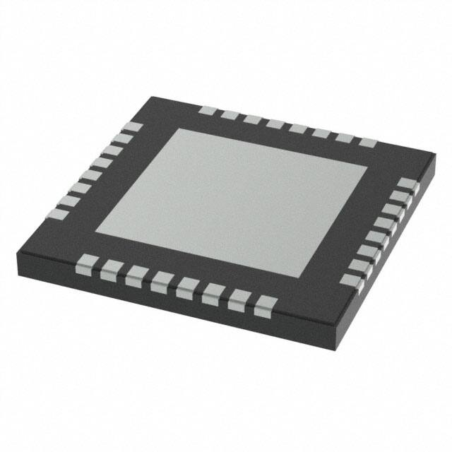


 工商网监
湘ICP备2023018690号
工商网监
湘ICP备2023018690号
