MAX20307
General Description
The MAX20307 is a configurable driver IC for enhancement
mode Gallium Nitride (eGaN) FETs, optimized for highfrequency operation. The device is designed to drive both
the high-side and low-side FETs in a half-bridge topology. The
floating high-side driver is capable of driving a high-side
eGaN FET operating up to 60V. A synchronous bootstrap
technique provides the high-side bias voltage and is
internally clamped at 5.2V. This clamping prevents the
gate voltage from exceeding the maximum rated gatesource voltage of eGaN FETs.
The gate driver input signal is 3.3V TTL logic compatible,
and can withstand input voltages up to 6V regardless of
the VCC voltage. Additionally, the MAX20307 features
adaptive dead time control.
High-frequency H-bridge drive capability and adaptive
dead time control make the MAX20307 ideal for highefficiency buck applications. TTL logic compatibility allows
the INH drive input to operate directly from the outputs of
most PWM controllers allowing for flexible design.
The device covers wireless power (transmitting) levels
from a few Watts to over 20 Watts making it well suited
for wireless charging of various portable devices. High
frequency optimization enables the use of wireless charging standards such as A4WP (6.78MHz) and ISM band
(13.56MHz) wireless charging.
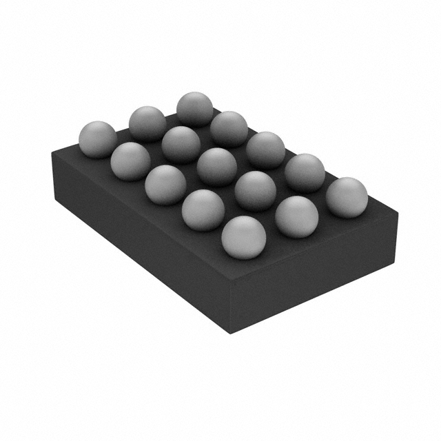
The MAX20307 is available in a space-saving, 15-bump,
1.2 x 2.0mm wafer-level package (WLP) and operate over
the -40°C to +85°C extended temperature range.
Applications
●● Switching Power Supply Topology Support
• Half and Full-Bridge converters
• Current Fed Push-Pull converters
• Synchronous Buck converters
●● A4WP Wireless Charging
●● Medical Device Wireless Charging in ISM Band
●● WPC and PMAT
19-100281; Rev 0; 3/18
High-Frequency Optimized
Configurable eGaN Driver
Benefits and Features
●● Flexible/Configurable Gate Drive
• Single Control Input
• 1A/5A Gate Source/Sink Current
●● High-Efficiency SMPS Design
• Low Loss Gate Drive: Optimized Bootstrap Circuit
• Automatic Dead Time Control Optimized for HalfBridge Converters
• Programmable Maximum Dead Time
• 0ns–9ns GPIO Controlled
• Fast Propagation Delay (22ns)
●● Safe Gate Drive
• High-Side Floating Node Voltage up to 60V
• Gate Supply Voltage UVLO
●● Space-Saving Design
• 0.4mm pitch 1.2mm x 2.0mm WLP
Ordering Information appears at end of data sheet.
�MAX20307
High-Frequency Optimized
Configurable eGaN Driver
Absolute Maximum Ratings
(Voltages reference to GND unless otherwise noted)
VCC...........................................................................-0.3V to +6V
VIN..........................................................................-0.3V to +66V
LO.................................................................-0.3V to VCC + 0.3V
HO......................................................VHS – 0.3V to VHB + 0.3V
HB..........................................................................-0.3V to +66V
HB to VCC..............................................................-0.3V to +60V
HS..........................................................................-0.3V to +60V
INL, INH, LDTY0, LDTY1, DTP0, DTP1..................-0.3V to +6V
Continuous Power Dissipation (TA = +70°C):
WLP (derate 16.4mW/°C above +70°C.)....................1312mW
Operating Temperature Range............................ -40°C to +85°C
Junction Temperature........................................ -40°C to +150°C
Storage Temperature Range............................. -40°C to +150°C
Soldering Temperature (reflow)........................................+260°C
Package Thermal Characteristics (Note 1)
WLP
Junction-to-Ambient Thermal Resistance (θJA)...........52°C/W
Note 1: Package thermal resistances were obtained using the method described in JEDEC specification JESD51-7, using a four-layer
board. For detailed information on package thermal considerations, refer to www.maximintegrated.com/thermal-tutorial.
Stresses beyond those listed under “Absolute Maximum Ratings” may cause permanent damage to the device. These are stress ratings only, and functional operation of the device at these
or any other conditions beyond those indicated in the operational sections of the specifications is not implied. Exposure to absolute maximum rating conditions for extended periods may affect
device reliability.
Electrical Characteristics
(VCC = 4.5 to 5.5V, TA = -40°C to +85°C unless otherwise noted. Typical values are at VCC = 5V, TA = +25°C.) (Note 2)
PARAMETER
SYMBOL
CONDITIONS
MIN
TYP
MAX
UNITS
5.5
V
13
mA
VCC
Supply Voltage Range
VCC
4.5
VCC Quiescent Current
IQ
INH = 0V
6
VCC Operating Current
ICC
f = 13.56MHz, CL = 47pF
35
VCC Undervoltage Lockout
(UVLO)
VCC_UVLO
VCC Rising
VCC_ UVLOHYS
VCC Falling
0.1
V
LO Output Low
LOOUT_LOW
ILO = 100mA
很抱歉,暂时无法提供与“MAX20307EWL+”相匹配的价格&库存,您可以联系我们找货
免费人工找货