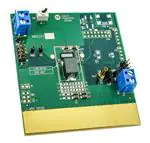
Evaluates: MAX20735
MAX20735 Evaluation Kit
General Description
The MAX20735 Evaluation Kit (EV kit) serves as a
reference platform for evaluating the MAX20735
voltage regulator IC. This single-chip, integrated switching
regulator provides an extremely compact, low-cost, highly efficient, fast, accurate and reliable power delivery
solution for emerging low-output voltage applications up
to 40A. Refer to the MAX20735 IC data sheet for more
information.
The EV kit consists of a fully assembled and tested
PCB implementation of the MAX20735. Jumper pins,
test points, and input/output connectors are included for
flexibility and ease-of-use in a wide range of applications.
The evaluation board is configured with an “edge strip” to
allow high di/dt loading when evaluating the system. The
+VOUT connection is on the top side, while the return (or
-VOUT) is on the bottom side, directly mirroring the topside strip.
Either solder directly to the output “strip” or use the J8
terminal block to interface to a load.
Features
●● High Efficiency and Power Density
●● Low Component Count
●● Small Solution Size
• 509mm2 Including Inductor and Output Capacitors
●● Optimized Performance
●● Reduced Design-In Time
●● Proven PCB Layout
●● Fully Assembled and Tested
Ordering Information appears at end of data sheet.
19-8622; Rev 0; 8/16
Getting Started
Required Equipment
●● MAX20735 EV kit
●● 4.5V to 16V power supply
●● 0A to 40A Load
●● Oscillocope, probes, voltmeter
Procedure
The EV kit is fully assembled and tested. Follow the steps
below to verify board operation:
1) Connect a powered-off 4.5V to 16V input supply to J1.
• Optionally, connect supply sense leads to VDD1
and GND1 for best accuracy.
2) Connect the load to J3 or J8.
3) Connect the VOUT scope probe/voltmeter to J4 or
J11, as desired.
• J4 and J11 are connected to the sense point for
best accuracy.
4) Position the SW1 toggle switch, pointing away from
J1 to enable the IC (if desired).
5) Turn on the power supply and observe that VOUT =
1V.
6) For efficiency measurements, J6 has appropriate
Kelvin sense points.
�Evaluates: MAX20735
MAX20735 Evaluation Kit
Operation
Input-Voltage Monitoring
The MAX20735 IC is a monolithic, high-frequency stepdown switching regulator optimized for applications
requiring small-size, high-efficiency, and low-output voltages. Detailed product and application information is
provided in the MAX20735 IC data sheet.
The VDD1 and GND1 sense points monitor the input supply.
Output Enable (OE)
J4-1 and J4-2 monitor the output voltage of VOUT and
GND, respectively. These test points should not be used
for loading. Alternatively, scopejack J11 can be used to
monitor the output voltage.
OE is used to enable/disable the output voltage. The
output voltage is enabled/disabled by SW1. Pointing SW1
in the direction of the silkscreened arrow enables the
regulator.
Output-Voltage Selection
The EV kit is setup to initially boot up to an output
voltage of 1V. This has been accomplished by setting
the reference to come up to a VBOOT of 0.6484V and
placing a voltage-divider in the feedback path with a
divide ratio of 0.6484. For different VOUT values, the
VBOOT and feedback-divider ratio can be changed, as
described in the MAX20735 IC data sheet.
RGAIN and COUT can also be changed to affect
performance. Refer to the MAX20735 IC data sheet for
more details.
Soft-Start and Switching Frequency
These are programmable parameters. For the EV kit, softstart is set to 3ms, and switching frequency to 400kHz.
Status Monitoring
Whenever the part is actively regulating, and the output
voltage is within the power-good window, the STAT pin
is high. In all other conditions, including enabled but in
a fault state, the STAT pin is pulled low. Refer to the
MAX20735 IC data sheet for more details.
www.maximintegrated.com
Switching-Voltage Monitoring
The switching waveform can be monitored on VX1.
Output-Voltage Monitoring
Efficiency Testing
●●
J6 provides convenient access to the appropriate
VIN and VOUT sense points.
●●
VIN_EFF± are on J6 pins 1 and 2.
●●
VOUT_EFF± are on J6 pins 3 and 4.
●●
Input and output currents should be measured with
0.1% lab shunts.
●● For increased accuracy, shunt mismatch can be
measured and calibrated out by doing a test running
the same current through both shunts.
●● For increased accuracy, shunt mismatch can be
measured and calibrated out by doing a test running
the same current through both shunts.
Ordering Information
DEVICE TYPE
MAX20735EVKIT#
#Denotes RoHS compliant.
TYPE
EV Kit
Maxim Integrated │ 2
�Evaluates: MAX20735
MAX20735 Evaluation Kit
MAX20735 Bill of Materials
Part Reference
Quantity
Description
C1, C74, C75
3
100uF, 25V, 20%, TANTALUM
C24
1
0.01uF, 25V, 10%, X7R
C3
1
0.1uF, 25V, 10%, X7R
C32
1
1000pF, 50V, 10%, X7R
C5, C6, C10, C11
4
47uF, 25V, 20%, X5R
C50
1
22uF, 6.3V, 20%, X6S
C60, C61
2
1.0uF, 25V, 20%, X5R
C62, C63, C66, C67, C69, C70, C71, C76, C77
9
100uf, 6.3V, 20%, X5R
C7
1
1uF, 25V, 10%, X7R
C8
1
0.22uF, 16V, 10%, X7R
C9, C36, C51
3
10uF, 6.3V, 20%, X5R
GND1, GND2, GND3, LOOP, VDD1, VX1
6
1_PIN-1X1 Straight
J1, J8
2
2_PIN-2 Pin, Terminal Block w/Screws, Blue
J11
1
Shielded Scope Probe Jack, Vertical
J3
1
2_Pin-Edge Fingers
J4
1
VOUT-DIF-1X2 Straight
J6
1
8_PIN-2X4 Straight
J7
1
6_PIN-2X3 Straight
L1
1
170nH, 10%, Isat= 66A
R1
1
1.78KΩ, 1%, 1/16W
R10, R20, R21, R22, R23
5
1KΩ, 5%, 1/16W
R11, R14
2
0Ω, 5%, 1/16W
R2
1
162KΩ, 1%, 1/16W
R3
1
2.67KΩ, 1%, 1/16W
R4
1
10Ω, 1%, 1/16W
R5, R8
2
20KΩ, 5%, 1/16W
R6
1
1.87KΩ, 1%, 1/16W
R9
1
3.48KΩ, 1%, 1/16W
SW1
1
DPDT-DPDT, 6pins, 1switch
U1
1
MAX20735
1
PCB# 35-900335-01-00
www.maximintegrated.com
Maxim Integrated │ 3
�2,3
2
2
3
3
2
PGM2
STAT
OE
VCC3
VCC2
VOUT
C32
1000pF
0402
OE
R15 0402
C51
10uF
X5R
0402
Rgain = 1.6m-ohm
Valley OCP = 35A
Fsw = 400kHz
15
13
PGM3
STAT
L2
VCC2
VCC3
OE
STAT
PGM3
PGM2
VOUT
VSENSE-
VSENSE+
MAX20735
VX
BST
U1
Do Not Stuff
MTG1
Do Not Stuff
MTG2
Combo footprint to fit L1 or L2
VX
12
14
VCC
PGM1
C31
Do Not Stuff
0402
PGM2
VCC2
VCC3
9
3
OE
4
PGM2
C36
10uF
X5R
0402
PGM1
Tstat = 125us
OTP = 150C
Freq Band = Even
C23
R3
Do Not Stuff 2.67K
0402
0402
PGM3
Do Not Stuff
C4
R2
Do Not Stuff 162K
0402
0402
PGM1
PMBus Addr = 0
Tss = 3ms
Vboot = 0.65V
R1
1.78K
0402
20K
R8 0402
2,3
PGM3
STAT
2
PGM1
3.3V
20K
R5 0402
VCC
2,3
C9
10uF
X5R
0402
2,3
3.3V
C7
1uF
X7R
0603
VX
VSENSE+
VSENSE-
1
2
Do Not Stuff
HS1
BST
7
C8
0.22uF
X7R
0402
8
C3
0.1uF
X7R
0402
Do Not Stuff
TIM1
Diff Pair
R12
Do Not Stuff
0402
170nH
L1
GND2
VX1
R10
1K
0402
C5
47uF
X5R
1206
1
2
1
GND_POWER
VDDH
5
VDDH
10
VCC
AGND
11
GND
6
R9
3.48K
0402
C39
R6
Do Not Stuff 1.87K
0402
0402
0 0402
C11
47uF
X5R
1206
C38
Do Not Stuff
0402
R13
Do Not Stuff
0402
SENSE_VOUT
C10
47uF
X5R
1206
C37
Do Not Stuff
0402
R14
C6
47uF
X5R
1206
Diff Pair
0 0402
R11
10
R4 0402
J4
VOUT-DIF
C24
0.01uF
0402
C71
100uf
1206
C68
Do Not Stuff
1206
VDD1
C76
100uf
1206
C69
100uf
1206
C66
100uf
1206
C63
100uf
1206
1
SNS
C77
100uf
1206
C70
100uf
1206
C67
100uf
1206
VOUT
C50
22uF
0805
C41
Do Not Stuff
0805
C30
C49
Do Not Stuff Do Not Stuff
0805
0805
C45
C48
Do Not Stuff Do Not Stuff
0805
0805
+
C29
Do Not Stuff
C28
Do Not Stuff
C43
Do Not Stuff
0805
C42
Do Not Stuff
0805
38-900335-01-00-07
+
C20
Do Not Stuff
0805
VOUT
Vin Sense-
Vin Sense+
C64
Do Not Stuff
1206
GND1
Vin Supply
1
C52
C47
C44
C12
C53
C16
C46
Do Not Stuff Do Not Stuff Do Not Stuff Do Not Stuff Do Not Stuff Do Not Stuff Do Not Stuff
0805
0805
0805
0805
0805
0805
0805
C33
C40
C34
Do Not Stuff Do Not Stuff Do Not Stuff
0805
0805
0805
C27
C19
C15
Do Not Stuff Do Not Stuff Do Not Stuff
0805
0805
0805
C65
Do Not Stuff
1206
J1
C26
C18
C14
Do Not Stuff Do Not Stuff Do Not Stuff
0805
0805
0805
1
2
C62
100uf
1206
+ C75
100uF
VDDH
C22
C17
C13
Do Not Stuff Do Not Stuff Do Not Stuff
0805
0805
0805
+ C2
+ C72
+ C73
+ C74
Do Not Stuff
Do Not Stuff
Do Not Stuff
100uF
LOOP
+ C1
100uF
1
www.maximintegrated.com
1
2
VDDH
MAX20735 Evaluation Kit
Evaluates: MAX20735
MAX20735 Schematics
Maxim Integrated │ 4
�1,3
1
1,3
1,3
1
1
1,3
1,3
1
PGM1
PGM3
PGM2
STAT
OE
VCC3
VCC2
VOUT
1,3
3.3V
VDDH
1K
R21
1K
R20
VIN_EFF-
C60
1.0uF
0402
25V
X5R
VIN_EFF+
VIN_EFFVOUT_EFF2
4
6
8
J6
1
3
5
7
1K
R23
1K
R22
VIN_EFF+
VOUT_EFF+
VOUT
Efficiency Test
1
2
+
VOUT_EFF-
C61
1.0uF
0402
25V
X5R
4
2
4
6
BYPASS
ON/OFF
C56
Do Not Stuff
C58
Do Not Stuff
X7R
0402
VOUT_EFF+
Do Not Stuff
J9
C35
Do Not Stuff
X7R
0603
3
OE
STAT
J7
1
1
3
5
PGM1
PGM3
PGM2
5
C57
Do Not Stuff
X5R
0402
12VB
LP2992AIM5-3.3/NOPB
U3
Vout
Vin
GND
2
GND3
6
4
3
1
SW3
1
1
5
2
3.3V
VDDH
6
4
3
1
5
2
Enable
SW1
OE
VOUT
3
4
Do Not Stuff
SW4
2
J11
3
1
2
J8
R26
2
1
J3
2
1
2_Pin
PGM3
Do Not Stuff
38-900335-01-00-07
SCOPE_PROBE_JACK
2
1
Vboot Restore
1
GND_POWER
+VOUT
www.maximintegrated.com
GND
VDDH
1,3
MAX20735 Evaluation Kit
Evaluates: MAX20735
MAX20735 Schematics (continued)
Maxim Integrated │ 5
�www.maximintegrated.com
1
2
Do Not Stuff
C705
Do Not Stuff
X700
Do Not Stuff
C702
1
2
3
4
5
6
7
8
9
10
11
12
13
14
D700
R709
Do Not Stuff
D701
Do Not Stuff
C703
Do Not Stuff
C706
Do Not Stuff
Do Not Stuff
MCLR/Vpp/RE3
RB7/KBI3/PGD
RA0/AN0
RB6/KBI2/PGC
RA1/AN1
RB5/KBI1/PGM
RA2/AN2/Vref-/CVref
RB4/AN11/KBI0
RA3/AN3/Vref+
RB3/AN9/CCP2(1)/VPO
RA4/T0CKI/C1OUT/RCV
RB2/AN8/INT2/VMO
RA5/AN4/SS/HLVDIN/C2OUTRB1/AN10/INT1/SCK/SCL
Vss
RB0/AN12/INT0/FLT0/SDI/SDA
OSC1/CLKI
Vdd
OSC2/CLKO/RA6
Vss
RC0/T1OSO/T13CKI
RC7/RX/DT/SDO
RC1/T1OSI/CCP2(1)/UOE
RC6/TX/CK
RC2/CCP1
RC5/D+/VP
Vusb
RC4/D-/VM
U700
Do Not Stuff
Do Not Stuff
R705
R700
MCLR
R704
C700
Do Not Stuff
Do Not Stuff
R703
Do Not Stuff
5VUSB
28
27
26
25
24
23
22
21
20
19
18
17
16
15
PGD
PGC
SWI
2
4
6
8
10
12
14
16
R715 Do Not Stuff
R714 Do Not Stuff
R713 Do Not Stuff
R710 Do Not Stuff
R708 Do Not Stuff
1
3
5
7
9
11
13
15
VCC2
VCC3
MAXPOWERTOOL002#
Do Not Stuff
J704
C707
Do Not Stuff
5VUSB
ALERT
Do Not Stuff
R702
C704
Do Not Stuff
C701
Do Not Stuff
R701
Do Not Stuff
6
7
8
9
1
2
3
4
5
J702
USB
USB 4pin
Do Not Stuff
CABLE1
Do Not Stuff
MTG1
MTG2
MTG3
MTG4
1
2
3
4
5
1
2
3
4
R707
R706
Do Not Stuff Do Not Stuff
J701
SWI
GND
PGC
PGD
MCLR
5VUSB
Serial
ALERT
3.3V
1
2
3
4
5
Programming
Do Not Stuff
J703
GND_POWER
VCC3
R719 Do Not Stuff
VCC2
R720 Do Not Stuff
PGM3
DNS
R721 Do Not
Stuff
PGM2
R722
Do Not Stuff
R723 Do Not Stuff
1,2
1
1
1,2
1,2
1,2
38-900335-01-00-07
MAX20735 Evaluation Kit
Evaluates: MAX20735
MAX20735 Schematics (continued)
Do Not Stuff
Data IN
Maxim Integrated │ 6
�MAX20735 Evaluation Kit
Evaluates: MAX20735
MAX20735 PCB Layer
Top Silkscreen
Bottom Silkscreen
www.maximintegrated.com
Maxim Integrated │ 7
�MAX20735 Evaluation Kit
Evaluates: MAX20735
MAX20735 PCB Layer (continued)
Layer 1
Layer 2
www.maximintegrated.com
Maxim Integrated │ 8
�MAX20735 Evaluation Kit
Evaluates: MAX20735
MAX20735 PCB Layer (continued)
Layer 3
Layer 4
www.maximintegrated.com
Maxim Integrated │ 9
�Evaluates: MAX20735
MAX20735 Evaluation Kit
Revision History
REVISION
NUMBER
REVISION
DATE
0
8/16
DESCRIPTION
Initial release
PAGES
CHANGED
—
For pricing, delivery, and ordering information, please contact Maxim Direct at 1-888-629-4642, or visit Maxim Integrated’s website at www.maximintegrated.com.
Maxim Integrated cannot assume responsibility for use of any circuitry other than circuitry entirely embodied in a Maxim Integrated product. No circuit patent licenses
are implied. Maxim Integrated reserves the right to change the circuitry and specifications without notice at any time.
Maxim Integrated and the Maxim Integrated logo are trademarks of Maxim Integrated Products, Inc.
© 2016 Maxim Integrated Products, Inc. │ 10
�


 工商网监
湘ICP备2023018690号
工商网监
湘ICP备2023018690号
