Click here to ask an associate for production status of specific part numbers.
MAX22515
IO-Link Transceiver with Integrated Protection
General Description
Benefits and Features
The MAX22515 low-power industrial transceiver can operate as either an IO-Link device or an IO-Link master transceiver in industrial applications. The MAX22515 features
a selectable control interface (pin mode or I2C), two integrated linear regulators, and integrated surge protection
for robust communication. The transceiver includes one
C/Q input-output channel and one digital input (DI) channel.
● High Configurability and Integration Reduces SKU
• Operates from 8V to 36V
• Auxiliary Digital Input (DI)
• I2C or Pin Mode Control
• Selectable C/Q Driver Current: 50mA to 250mA
• Selectable C/Q Driver Slew Rate (I2C Mode)
• Integrated Oscillator for IO-Link Communication
• IO-Link Wake-Up Detection and Wake-Up
• Generation
• Integrated Linear Regulators: 3.3V and 5V
• Compatible Register Set to MAX22513
• Able to Communicate at COM1, COM2, and COM3
Data Rates
The device features a flexible control interface. Pin-control
logic inputs allow for operation with switching sensors that
do not use a microcontroller. For sensors that use a microcontroller, an I2C interface is available providing extensive configuration and diagnostics. Additionally, an integrated oscillator simplifies the clock generation for IO-Link
devices.
The MAX22515 features extensive integrated protection
to ensure robust communication in harsh industrial environments. All IO-Link line interface pins (V24, C/Q, DI,
and GND) are reverse voltage protected, short-circuit protected, hot-plug protected, and feature integrated ±1.2kV/
500Ω surge protection.
The MAX22515 is available in a tiny WLP package
(2.5mm x 2.0mm) or a 24-pin TQFN-EP package (4mm x
4mm) and operates over the -40ºC to +125ºC temperature
range.
Applications
● IO-Link Sensor and Actuator Devices
● Industrial Sensors
● IO-Link Masters
Ordering Information appears at end of data sheet.
● Integrated Protection Enables Robust Systems
• ±1.2kV/500Ω Surge Protection on V24, C/Q, DI, and
GND
• Reverse Polarity Protection on V24, C/Q, DI, and
GND
• Hot-Plug Protection on Supply Input (V24)
• Glitch Filters for Improved Burst Resilience
• Selectable Driver Overcurrent Configuration
• -40°C to +125°C Operating Temperature Range
• Fast Demagnetization of Inductive Loads
● Optimized for Small Designs
• Low Power Dissipation: 2Ω (typ) C/Q Driver OnResistance
• 1.3mA (typ) Supply Current
• Available in Two Tiny Packages:
• 20-Bump WLP (2.5mm x 2.0mm)
• 24-Pin TQFN-EP (4mm x 4mm)
19-100567; Rev 7; 4/21
© 2021 Analog Devices, Inc. All rights reserved. Trademarks and registered trademarks are the property of their respective owners.
One Analog Way, Wilmington, MA 01887 U.S.A. | Tel: 781.329.4700 | © 2021 Analog Devices, Inc. All rights reserved.
�MAX22515
IO-Link Transceiver with Integrated Protection
Simplified Block Diagram
VL
LOGIC
SUPPLY
A0/CLKEN
MCLK
DIVIDER
V33
LIN
V5
3.3V LINEAR
REGULATOR
5V LINEAR
REGULATOR
29.49MHz
OSCILLATOR
INTEGRATED
PROTECTION
V24
MAX22515
EN/POK
SCL/100MA
SDA/WU
WU/IRQ
CONTROL
INTERFACE
WAKE-UP
DETECTION
INTEGRATED
PROTECTION
C/Q
TRANSCEIVER
C/Q
I2C/PIN
TX
TXEN
RX
INTEGRATED
PROTECTION
LI
SGND
www.analog.com
DI
GND
Analog Devices | 2
�MAX22515
IO-Link Transceiver with Integrated Protection
Absolute Maximum Ratings
All voltages referenced to GND, unless otherwise noted. ............
V24 (Continuous) ..................................................... -36V to +36V
V24 (Peak, 100μs) ................................................... -52V to +65V
LIN (LIN is connected to V24, Continuous).............. -36V to +36V
LIN (LIN is connected to V24, Peak)........................ -52V to +65V
LIN ................................................... max(-0.3V, V5 - 0.3V) to V24
C/Q (Continuous) ...... max(-36V, V24 - 36V) to min(+36V, (V24 +
36V)
C/Q (Peak, 100μs) ......max(-52V, V24 - 52V) to min (+52V, V24 +
52V)
DI (Continuous) ....................................................... -36V to +36V
DI (Peak, 100μs) ..................................................... -52V to +52V
V5, VL ....................................................................... -0.3V to +6V
V33................................................................. -0.3V to (V5 + 0.3V)
LOGIC PINS
I2C/PIN, EN/POK, CLKEN, SCL/100MA,..................................
SDA/WU, WU/IRQ, TXEN, TX .............................. -0.3V to +6V
MCLK, RX, LI .................................................. -0.3V to (VL+0.3)V
SGND..................................................................... -0.3V to +0.3V
Continuous Current into V24 and GND ...................................±1A
Continuous Current into LIN ............................................±100mA
Continuous Current into C/Q............................................±500mA
Continuous Current into V5 and V33 ..................................±60mA
Continuous Current into Any Other Pin..............................±50mA
Continuous Power Dissipation 24-Pin TQFN (TA = +70ºC)
(derate at 27.8mW/ºC above +70ºC) ...........................2222mW
20-bump WLP (TA = +70ºC)
(derate at 21.35mW°/C above +70ºC).........................1700mW
Operating Temperature Range ...........................-40ºC to +125ºC
Maximum Junction Temperature ...................................... +160ºC
Storage Temperature Range .............................. -65ºC to +150ºC
Soldering Temperature (TQFN only, 10 sec) .................... +300ºC
Bump Reflow Temperature ............................................... +260ºC
Stresses beyond those listed under “Absolute Maximum Ratings” may cause permanent damage to the device. These are stress ratings only, and functional operation of the
device at these or any other conditions beyond those indicated in the operational sections of the specifications is not implied. Exposure to absolute maximum rating conditions for
extended periods may affect device reliability.
Package Information
24 TQFN-EP
Package Code
T2444+4
Outline Number
21-0139
Land Pattern Number
90-0022
THERMAL RESISTANCE, SINGLE-LAYER BOARD
Junction-to-Ambient (θJA)
48°C/W
Junction-to-Case Thermal Resistance (θJC)
3°C/W
THERMAL RESISTANCE, FOUR-LAYER BOARD
Junction-to-Ambient (θJA)
36°C/W
Junction-to-Case Thermal Resistance (θJC)
3°C/W
20 (5 x 4) WLP
Package Code
W201L2+1
Outline Number
21-100314
Land Pattern Number
Refer to Application Note 1891
THERMAL RESISTANCE, FOUR-LAYER BOARD
Junction-to-Ambient (θJA)
46.83°C/W
For the latest package outline information and land patterns (footprints), go to www.maximintegrated.com/packages.
Note that a “+”, “#”, or “-” in the package code indicates RoHS status only. Package drawings may show a different
suffix character, but the drawing pertains to the package regardless of RoHS status.
Package thermal resistances were obtained using the method described in JEDEC specification JESD51-7, using a
four-layer board. For detailed information on package thermal considerations, refer to www.maximintegrated.com/
thermal-tutorial.
www.analog.com
Analog Devices | 3
�MAX22515
IO-Link Transceiver with Integrated Protection
Electrical Characteristics—DC
(V24 = 8V to 36V, V5 = 4.5V to 5.5V, VL = 2.5V to 5.5V, All logic inputs at VL or GND, TA = -40°C to +125°C, unless otherwise noted.
Typical values are at V24 = 24V, V5 = 5V, VL = 3.3V, and TA = +25°C, unless otherwise noted.) (Notes 1, 2)
PARAMETER
SYMBOL
CONDITIONS
MIN
TYP
MAX
UNITS
36
V
DC ELECTRICAL CHARACTERISTICS / POWER SUPPLY
V24 Supply Voltage
V24
V24 Undervoltage
Lockout Threshold
V24UVLO
V24 Undervoltage
Lockout Threshold
Hysteresis
V24UVLO_HYS
V24 Low Voltage
Warning Threshold
V24_W
V24 Supply Current
8
V24 rising
6.9
7.5
8
V24 falling
6.4
6.9
7.5
500
T
I24
V5 Supply Voltage
V5
V5 Undervoltage
Lockout Threshold
V5UVLO
V24 falling
V5 powered
externally, no load
on C/Q
VL Logic Level Supply
Voltage
VL Undervoltage
Threshold
I5
16.3
C/Q is high
impedance
16
30
C/Q is in push-pull
and is high or low
285
400
C/Q is high
impedance, V33 is
disabled, MCLK is
disabled
560
850
C/Q is in push-pull
mode and is high
or low, V33 is
enabled, MCLK is
disabled
1.08
1.5
C/Q is in push-pull
mode and is high
or low, V33 is
enabled, MCLK is
enabled
1.5
2.5
VL rising
IVL
All logic inputs at
GND or VL, no load
on any logic output
V
V
μA
mA
0.5
MCLK disabled
VL Logic Level Supply
Current
5.5
3
VL
VLUVLO
4.5
3.5
V5 falling
V
μA
V5 rising
LIN = V5, V5 is
powered externally,
no load on V33, no
load on C/Q
mV
15.3
LIN = V5, V5 supplied externally
LIN = V5, V5 is
powered externally,
no load on V33, no
load on C/Q
V5 Supply Current
14.5
V
2.2
5.5
V
0.85
1.2
V
1
10
MCLK enabled, f =
29.49MHz
800
MCLK enabled,
10pF load on
MCLK, VL = 3.3V, f
= 29.49MHz
1.56
μA
mA
DC ELECTRICAL CHARACTERISTICS / 5V LINEAR REGULATOR (V5)
V5 Input Supply Voltage
V5 Output Voltage
V5 Load Regulation
www.analog.com
VLIN
V5
∆V5_LDR
8
8V ≤ VLIN ≤ 36V, no load on V5
VLIN = 24V, 1mA ≤ ILOAD ≤ 50mA
4.9
36
V
5
5.1
V
0.8
2
%
Analog Devices | 4
�MAX22515
IO-Link Transceiver with Integrated Protection
Electrical Characteristics—DC (continued)
(V24 = 8V to 36V, V5 = 4.5V to 5.5V, VL = 2.5V to 5.5V, All logic inputs at VL or GND, TA = -40°C to +125°C, unless otherwise noted.
Typical values are at V24 = 24V, V5 = 5V, VL = 3.3V, and TA = +25°C, unless otherwise noted.) (Notes 1, 2)
PARAMETER
SYMBOL
V5 Line Regulation
∆V5_LNR
8V ≤ VLIN ≤ 36V, ILOAD = 1mA
V5 Power Supply
Rejection Ratio (PSRR)
PSRRV5
f = 100kHz, ILOAD = 20mA
V5 Load Capacitance
CV5
CONDITIONS
External capacitance required on V5
MIN
TYP
MAX
UNITS
0.007
0.3
mV/V
-65
dB
0.8
1
μF
3.22
3.32
3.42
V
0.1
0.8
%
DC ELECTRICAL CHARACTERISTICS / 3.3V LINEAR REGULATOR (V33)
V33 Output Voltage
V33 Load Regulation
V33 Load Capacitance
V33
∆V33_LR
CV33
No load
1mA ≤ ILOAD ≤ 50mA
External capacitance required on V33
0.8
1
µF
DC ELECTRICAL CHARACTERISTICS / C/Q DRIVER
C/Q Driver OnResistance
C/Q Driver Current Limit
ROH
High-side enabled, CL[1:0] = 11, ILOAD =
-200mA (Note 3)
2.65
4.6
ROL
Low-side enabled, CL[1:0] = 11, ILOAD =
+200mA (Note 3)
2.2
4.2
ICL
VDROP = 3V
(Note 4)
Ω
CL[1:0] = 00
50
66
80
CL[1:0] = 01
(I2C mode) or SDA/
100MA = high (pin
mode)
100
120
140
CL[1:0] = 10
(I2C mode) or SDA/
100MA = low (pin
mode)
210
240
270
CL[1:0] = 11
260
300
340
mA
I2C mode only, V24 = 24V, (V24 - 36V) ≤
C/Q Leakage Current
ILEAK_CQ
VC/Q ≤ 36V,
C/Q driver and receiver disabled
(CQ_EN = 0, RXDIS = 1)
-40
+30
µA
C/Q driver disabled (CQ_EN = 0), V24 =
24V, 0 ≤ VC/Q ≤ (V24 - 0.5V)
-2
+2
-90
+300
µA
C/Q Output Reverse
Current
IREV_CQ
C/Q driver enabled (TXEN = high, CQ_
EN = 1) and in push-pull
(CQ_PP = 1), VC/Q = (V24 + 5V) or
(VGND - 5V)
C/Q Weak Pulldown
Current
IPD
I2C mode only, VC/Q > 5V, TXEN = low,
CQ_EN = 1, CQ_PD = 1, CQ_PU = 0
(Note 5)
+230
+320
+400
µA
C/Q Weak Pullup
Current
IPU
I2C mode only,VC/Q = (V24 - 5V), TXEN
= low, CQ_EN = 1, CQ_PD = 0, CQ_PU
= 1 (Note 5)
-400
-300
-230
µA
DC ELECTRICAL CHARACTERISTICS / C/Q, DI RECEIVER
Input Voltage Range
Input Threshold High
www.analog.com
VIN
VTH
For valid RX/LI logic
TXEN = low
V24-36
36
V
V24 ≥ 18V
10.8
12.5
V
V24 < 18V
57.5
72
% of V24
Analog Devices | 5
�MAX22515
IO-Link Transceiver with Integrated Protection
Electrical Characteristics—DC (continued)
(V24 = 8V to 36V, V5 = 4.5V to 5.5V, VL = 2.5V to 5.5V, All logic inputs at VL or GND, TA = -40°C to +125°C, unless otherwise noted.
Typical values are at V24 = 24V, V5 = 5V, VL = 3.3V, and TA = +25°C, unless otherwise noted.) (Notes 1, 2)
PARAMETER
Input Threshold Low
Input Hysteresis
SYMBOL
CONDITIONS
VTL
TXEN = low
VHYS
TXEN = low
MIN
TYP
MAX
UNITS
V24 ≥ 18V
8.8
10.5
V
V24 < 18V
45
63
% of V24
V24 ≥ 18V
2
V
V24 < 18V
11
% of V24
C/Q Input Capacitance
CIN_CQ
Driver disabled, CQ_EN = 0, RXDIS = 0,
CQ_PD = 0, CQ_PU = 0,
f = 100kHz
45
pF
DI Input Capacitance
CIN_DI
DIDIS = 0, LIDIS = 0, f = 100kHz
4
pF
IDI_IN
V24 = 24V, DI receiver enabled, (V24 36V) ≤ VDI ≤ 36V
DI Input Current
-10
+15
µA
DC ELECTRICAL CHARACTERISTICS / LOGIC INPUTS (A0/CLKEN, SCL/100MA, SDA/WU, TXEN, TX, I2C/PIN, EN/POK)
Logic Input Voltage Low
VIL
Logic Input Voltage High
VIH
0.2 x VL
0.7 x VL
Logic Input Leakage
Current
ILEAK
A0/CLKEN, SCL/100MA, SDA/WU,
TXEN, TX, I2C/PIN, Logic input = GND or
VL
EN/POK Input Pullup
Resistance
RPU
EN/POK
-1
60
V
V
100
+1
μA
140
kΩ
0.15
V
DC ELECTRICAL CHARACTERISTICS / LOGIC OUTPUTS (WU/IRQ, MCLK, SDA/WU, RX, LI)
Logic Output Voltage
Low
VOL
LI, RX, MCLK, SDA/WU, ILOAD = +5mA
Logic Output Voltage
High
VOH
LI, RX, MCLK, ILOAD = -5mA
VL - 0.2
Open-Drain High
Impedance Leakage
Current
ILK_OD
WU/IRQ, output not asserted
-1
+1
μA
RX, LI, MCLK, DIDIS = 1, RXDIS = 1,
MCLKDIS = 1, Logic output = GND or VL
-1
+1
μA
-1
+1
μA
Logic Output Leakage
Current
SDA/WU Leakage
Current
ILKG_OUT
ILK_SDA
V
DC ELECTRICAL CHARACTERISTICS / THERMAL MANAGEMENT
C/Q Driver Shutdown
Temperature
TSHUT_D
C/Q Driver Shutdown
Hysteresis
TSHUT_DHYS
IC Thermal Warning
Threshold
TWRN
IC Thermal Warning
Threshold Hysteresis
TWRN_HYS
IC Junction Thermal
Shutdown Threshold
TSHUT_IC
IC Junction Thermal
Shutdown Hysteresis
TSHUT_ICHYS
www.analog.com
Driver temperature rising, C/Q driver fault
bit is set and driver is disabled
+150
°C
Driver temperature falling, C/Q driver is
automatically reenabled
10
°C
Die temperature rising, THERMW and
THERMWINT bits are set
+140
°C
15
°C
Die temperature rising
+160
°C
Die temperature falling
15
°C
Die temperature falling, THERMW bit is
cleared
Analog Devices | 6
�MAX22515
IO-Link Transceiver with Integrated Protection
Electrical Characteristics—AC
(V24 = 8V to 36V, V5 = 4.5V to 5.5V, VL = 2.5V to 5.5V, All logic inputs at VL or GND, TA = -40°C to +125°C, unless otherwise noted.
Typical values are at V24 = 24V, V5 = 5V, VL = 3.3V, and TA = +25°C, unless otherwise noted.) (Notes 1, 2)
PARAMETER
SYMBOL
CONDITIONS
MIN
TYP
MAX
0.5
0.75
UNITS
AC ELECTRICAL CHARACTERISTICS / C/Q DRIVER
C/Q Driver Low-to-High
Propagation Delay
C/Q Driver High-to-Low
Propagation Delay
C/Q Driver Skew
C/Q Driver Rise Time
C/Q Driver Fall Time
tPDLH_PP
tPDLH_OC
tPDHL_PP
tPDHL_OC
tSKEW
tRISE
tFALL
CQSLEW[1:0] =
00, Figure 1
CQSLEW[1:0] =
00, Figure 1
NPN mode
Push-pull or PNP
mode,
V24(max) = 30V,
Figure 1
Push-pull or NPN
mode,
V24(max) = 30V,
Figure 1
μs
1
Push-pull or NPN
mode
0.45
PNP mode
|tPDLH – tPDHL|, CQSLEW[1:0] = 00
|tRISE - tFALL|,
Push-pull mode,
V24(max) = 30V
Difference in C/Q Rise
and Fall Time
Push-pull or PNP
mode
0.75
μs
1
-0.25
0.05
+0.25
CQSLEW[1:0] = 00
0.05
0.15
0.3
CQSLEW[1:0] = 01
(I2C mode) or
when in pin mode
0
0.3
0.84
CQSLEW[1:0] = 10
0.45
0.9
1.4
CQSLEW[1:0] = 11
1.5
3.3
6
CQSLEW[1:0] = 00
0.05
0.16
0.3
CQSLEW[1:0] = 01
(I2C mode) or
when in pin mode
0.15
0.33
0.5
CQSLEW[1:0] = 10
0.45
0.8
1.3
CQSLEW[1:0] = 11
1.5
3.3
6
CQSLEW[1:0] = 00
0.01
CQSLEW[1:0] = 01
(I2C mode) or
when in pin mode
0.03
CQSLEW[1:0] = 10
0.1
CQSLEW[1:0] = 11
0
μs
μs
μs
μs
C/Q Driver Enable Time
High
tENH
Push-pull or NPN configuration, Figure 2
0.5
0.75
μs
C/Q Driver Enable Time
Low
tENL
Push-pull or PNP configuration, Figure 3
0.2
0.4
μs
C/Q Driver Disable Time
High
tDISH
Push-pull or NPN configuration, Figure 2
1.8
μs
C/Q Driver Disable Time
Low
tDISL
Push-pull or PNP configuration, Figure 3
1.8
μs
AC ELECTRICAL CHARACTERISTICS / C/Q, DI RECEIVER
C/Q Receiver Low-toHigh Propagation Delay
tPRLH_CQ
Figure 4
C/Q Receiver High-toLow Propagation Delay
tPRHL_CQ
Figure 4
C/Q Receiver Skew
www.analog.com
RXFILTER = 1
0.85
1.35
1.8
RXFILTER = 0
0.25
0.38
0.55
RXFILTER = 1
0.85
1.28
1.8
RXFILTER = 0
0.2
0.3
0.5
RXFILTER = 1
70
RXFILTER = 0
70
μs
μs
ns
Analog Devices | 7
�MAX22515
IO-Link Transceiver with Integrated Protection
Electrical Characteristics—AC (continued)
(V24 = 8V to 36V, V5 = 4.5V to 5.5V, VL = 2.5V to 5.5V, All logic inputs at VL or GND, TA = -40°C to +125°C, unless otherwise noted.
Typical values are at V24 = 24V, V5 = 5V, VL = 3.3V, and TA = +25°C, unless otherwise noted.) (Notes 1, 2)
PARAMETER
SYMBOL
CONDITIONS
DI Receiver Low-to-High
Propagation Delay
tPRLH_DI
Figure 4
DI Receiver High-to-Low
Propagation Delay
tPRHL_DI
Figure 4
MIN
TYP
MAX
DIFILTER = 1
1.2
1.8
2.4
DIFILTER = 0
0.6
0.9
1.2
DIFILTER = 1
1.2
1.7
2.4
DIFILTER = 0
0.5
0.75
1.1
UNITS
μs
μs
AC ELECTRICAL CHARACTERISTICS / WAKE-UP DETECTION (Figure 5)
Wake-Up Input
Minimum Pulse Width
tWUMIN
CLOAD = 3nF
60
66
70
μs
Wake-Up Input
Maximum Pulse Width
tWUMAX
CLOAD = 3nF
85
95
110
μs
SDA/WU (Pin mode),
WU/IRQ (I2C Mode)
Output Low Time
tWUL
Valid wake-up condition on C/Q (Note 6)
150
200
250
μs
AC ELECTRICAL CHARACTERISTICS / WAKE-UP GENERATION (I2C mode only, Figure 6)
Setup Time before
Wake-Up
Wake-Up Pulse
Duration
tSU_WU
80
tWU
Wake-up pulse has opposite polarity of
the existing C/Q level
On-Time after Wake-Up
tON_WU
C/Q driver enabled with original polarity
after tWU
High Impedance Time
after Wake-Up
tDIS_WU
C/Q driver is high impedance after
tON_WU
C/Q Driver Current Limit
During Wake-Up Pulse
IWU
WURQ = 1, CLDIS = 0 or 1
75
80
μs
85
μs
2
μs
418
μs
500
mA
AC ELECTRICAL CHARACTERISTICS / MCLK CLOCK TIMING
MCLK Frequency
MCLK Duty Cycle
fMCLK
CLKDIV[2:0] = 000
3.612
3.686
3.761
CLKDIV[2:0] = 001
7.225
7.373
7.523
CLKDIV[2:0] = 010
14.45
14.74
15.05
CLKDIV[2:0] = 011
28.90
29.49
30.09
CLKDIV[2:0] = 100
1.806
1.843
1.881
DMCLK
50
MHz
%
AC ELECTRICAL CHARACTERISTICS / I2C TIMING SPECIFICATIONS (Figure 7)
Maximum I2C Clock
Frequency
fI2CCLK
Maximum Clock Period
tSCLMAX
100
μs
Bus Free Time Between
STOP and START
Condi- tions
tI2CBUF
0.16
μs
START Condition Setup
Time
tI2CSUSTA
0.05
μs
Repeat START
Condition Setup Time
tI2CSUSTA
90% to 90%
0.05
μs
START Condition Hold
Time
tI2CHDSTA
10% of SDA/WU to 90% of SCL/100MA
0.09
μs
www.analog.com
2
MHz
Analog Devices | 8
�MAX22515
IO-Link Transceiver with Integrated Protection
Electrical Characteristics—AC (continued)
(V24 = 8V to 36V, V5 = 4.5V to 5.5V, VL = 2.5V to 5.5V, All logic inputs at VL or GND, TA = -40°C to +125°C, unless otherwise noted.
Typical values are at V24 = 24V, V5 = 5V, VL = 3.3V, and TA = +25°C, unless otherwise noted.) (Notes 1, 2)
PARAMETER
STOP Condition Setup
Time
SYMBOL
tI2CSUSTO
CONDITIONS
MIN
TYP
MAX
UNITS
90% of SCL/100MA to 10% of SDA/WU
0.05
μs
Clock Low Period
tI2CLOW
10% to 10%
0.12
μs
Clock High Period
tI2CHIGH
90% to 90%
0.18
μs
Data Valid to SCL/
100MA Rise Time
tI2CSUDAT
Write Setup Time
50
ns
Data Hold Time
tI2CHDDAT
Write Hold Time
Maximum SDA/WU
Drive Low Time
tDATLOW
1.0
1.1
0
ns
1.2
ms
ESD AND EMC TOLERANCE
ESD Protection
(V24, C/Q, DI Pins)
IEC 61000-4-2 Contact Discharge, 500pF
load on C/Q, 1.5kΩ in series with DI
±4
kV
ESD Protection
(All Other Pins)
Human Body Model
±2
kV
±1.2
kV
Surge Protection
(V24, C/Q, DI, GND
Pins)
VSRG
IEC 61000-4-5, 500Ω, 8/20µs surge
Note 1:
Note 2:
Note 3:
Note 4:
All devices 100% production tested at TA = +25ºC. Limits over operating temperature range are guaranteed by design.
Currents out of the device are negative. Currents into the device are positive.
Not production tested. Guaranteed by design.
VDROP is measured as the voltage from the driver output to GND (VDRIVER - VGND) when measuring the low-side
drivercurrent limit and as (V24 - VDRIVER) when measuring the high-side current limit.
Note 5: When CQ_PD or CQ_PU are set to 1, the weak pullups and weak pulldowns are enabled in all C/Q operating modes:
transceiver in receive mode and driver in push-pull, NPN, or PNP modes
Note 6: SDA/WU always asserts when a valid wake-up condition is received when operating in pin mode. When operating the device
in I2C mode, WU/IRQ asserts for tWUL only when no interrupts have been registered (INTERRUPT register) and the WUM =
1 in the IRQMASK register. If WUM = 0, WUINT is set when a valid wake-up event is detected and WU/IRQ asserts until the
INTERRUPT register is read.
www.analog.com
Analog Devices | 9
�MAX22515
IO-Link Transceiver with Integrated Protection
V24
TXEN
TXEN
MAX22515
TX
5kΩ
MAX22515
TX
C/Q
3.3nF
GND
5kΩ
C/Q
3.3nF
GND
PUSH-PULL AND PNP MODE
NPN MODE
VL
TXEN
0V
VL
TX
50%
50%
tPDHL
C/Q
0V
tPDLH
80%
80%
20%
20%
V24
50%
tFALL
50%
0V
tRISE
Figure 1. C/Q Driver Propagation Delays
V24
TXEN
VL
5kΩ
MAX22515
C/Q
TX
GND
3.3nF
VL
TXEN
0V
tDISH
tENL
V24
C/Q
50%
10%
0V
Figure 2. C/Q Driver Enable Low and Disable High Timing
www.analog.com
Analog Devices | 10
�MAX22515
IO-Link Transceiver with Integrated Protection
TXEN
MAX22515
TX
C/Q
GND
3.3nF
5kΩ
VL
TXEN
0V
tDISL
tENH
V24
90%
C/Q
50%
0V
Figure 3. C/Q Driver Enable Time High and Disable Time Low
TXEN
C/Q,
DI
MAX22515
GND
RX,
LI
15pF
V24
C/Q,
DI
50%
50%
0V
tPRHL
tPRLH
RX,
LI
VL
50%
50%
0V
Figure 4. C/Q and DI Receiver Timing
www.analog.com
Analog Devices | 11
�MAX22515
IO-Link Transceiver with Integrated Protection
TXEN
TX
MAX22515
SDA/WU
WU/IRQ
C/Q
GND
TXEN
TX
< tWUMIN
NO WAKE-UP
C/Q
tWUMIN < tWU < tWUMAX
SDA/WU
WU/IRQ
tWUL
Figure 5. Wake-Up Detection Timing
www.analog.com
Analog Devices | 12
�MAX22515
IO-Link Transceiver with Integrated Protection
1
WURQ
BIT
0
C/Q
VOLTAGE
LOW-IMPEDANCE
C/Q DRIVER
STATE
HIGH-IMPEDANCE
HIGH-IMPEDANCE
tWU
tSU_WU
tON_WU
tDIS_WU
Figure 6. Wake-Up Generation Timing
PROTOCOL
BIT 7
MSB
(A7)
START CONDITION
(S)
tI2CLOW
BIT 0
LSB
(R/W)
BIT 6
(A6)
tI2CHIGH
ACKNOWLEDGE
(A)
STOP CONDITION
(P)
1/fSCL
tI2CSUSTA
SCL/100MA
tI2CSUSTO
tI2CBUF
SDA/WU
tI2CHDSTA
tI2CHDDAT
tI2CSUDAT
Figure 7. I2C Timing
www.analog.com
Analog Devices | 13
�MAX22515
IO-Link Transceiver with Integrated Protection
Typical Operating Characteristics
(V24 = 24V, LIN is connected to V24, VL = V33, TA = 25°C, unless otherwise noted.)
www.analog.com
Analog Devices | 14
�MAX22515
IO-Link Transceiver with Integrated Protection
Typical Operating Characteristics (continued)
(V24 = 24V, LIN is connected to V24, VL = V33, TA = 25°C, unless otherwise noted.)
www.analog.com
Analog Devices | 15
�MAX22515
IO-Link Transceiver with Integrated Protection
Pin Configurations
DI
LIN
V24
C/Q
GND
GND
TOP VIEW
18
17
16
15
14
13
N.C.
19
12
N.C.
LI
20
11
RX
I2C/PIN
21
10
TX
V5
22
9
TXEN
V33
23
8
SDA/WU
7
SCL/100MA
MAX22515
*EP
+
5
TQFN
4mm x 4mm
6
A0/CLKEN
4
GND
WU/IRQ
3
SGND
2
MCLK
1
VL
24
EN/POK
TOP VIEW
(BUMP SIDE DOWN)
MAX22515
1
2
3
4
5
A
SCL/
100MA
SDA/
WU
RX
TX
GND
B
SGND
A0/
CLKEN
TXEN
WU/
IRQ
C/Q
C
MCLK
EN/
POK
I2C/PIN
LIN
V24
D
VL
V33
V5
LI
DI
+
WLP
Pin Description
PIN
TQFN
WLP
NAME
FUNCTION
POWER
1
D1
VL
4
B1
SGND
www.analog.com
Logic Supply Input. Bypass VL to GND with a 0.1μF capacitor as close to the
device as possible. VL sets the logic level for all logic signals. Connect VL to V33,
V5, or to an external voltage between 2.5V and 5V.
Signal Ground. Connect SGND to GND.
Analog Devices | 16
�MAX22515
IO-Link Transceiver with Integrated Protection
Pin Description (continued)
PIN
NAME
FUNCTION
TQFN
WLP
5, 13, 14
A5
GND
Ground
16
C5
V24
Supply Voltage Input. Apply a 24V (typ) supply to V24. Bypass V24 to GND with a
10nF capacitor as close to the device as possible.
LIN
5V Linear Regulator Input. Bypass LIN to GND with a 10nF capacitor as close to
the device as possible. Connect LIN to V24 or to an external supply between 8V
and 36V. Short LIN to V5 to disable the internal regulator. Connect 5V to LIN and
V5 when the internal regulator is disabled.
17
C4
22
D3
V5
5V Linear Regulator Output/Supply Input. Bypass V5 to GND with a 1μF capacitor
as close to the device as possible. V5 is the output of the internal 5V linear
regulator. To disable the internal regulator, connect LIN to V5. 5V is required on
V5 for normal operation. If the 5V regulator is disabled, apply an external 5V
power supply to V5.
23
D2
V33
3.3V Linear Regulator Output. Bypass V33 to GND with a 1μF capacitor as close
to the device as possible. V33 is not required for normal operation.
EP
-
EP
Exposed Pad (TQFN Only). Connect EP to GND.
24V LINE INTERFACE
IO-Link Transceiver Input/Output.
15
B5
C/Q
I2C Mode: C/Q is disabled at startup. Set CQ_EN = 1 and drive TXEN high to
enable the C/Q driver.
Pin mode: Drive TXEN high to enable the C/Q driver.
Auxiliary Digital Input.
18
D5
DI
I2C Mode: DI is enabled at power-up. Disable DI by setting the DIDIS bit in the
CONTROL register.
Pin mode: DI is enabled and cannot be disabled.
CONTROL INTERFACE
IO-Link Wake-Up Detection/Interrupt Open-Drain Output.
2
B4
WU/IRQ
I2C Mode: WU/IRQ asserts low when a valid IO-Link wake-up is detected on the
C/Q line or when a bit in the INTERRUPT register is set.
Pin mode: WU/IRQ asserts low when a thermal or overcurrent fault occurs.
WU/IRQ deasserts when the fault is no longer present.
I2C Address Select/MCLK Enable Input.
6
B2
A0/CLKEN
I2C Mode: Connect A0/CLKEN high or low to set the I2C address for the
MAX22515. See the I2C Controller Interface section for more information.
Pin mode: Drive A0/CLKEN high to enable the clock output on MCLK. Drive A0/
CLKEN low to disable the clock output. MCLK is 14.74MHz (typ) in pin mode.
MCLK is high impedance when disabled.
I2C Serial Clock/C/Q Driver Current Limit Setting Input.
7
A1
SCL/100MA
I2C Mode: I2C interface clock input.
Pin mode: Drive SCL/100MA high to set the C/Q driver current limit to 100mA
(min). Drive SCL/100MA low to set the driver current limit to 200mA (min).
www.analog.com
Analog Devices | 17
�MAX22515
IO-Link Transceiver with Integrated Protection
Pin Description (continued)
PIN
TQFN
WLP
NAME
FUNCTION
I2C Serial Data Input/Ouput/Wake-Up Detection Output.
8
A2
SDA/WU
I2C Mode: I2C serial data input/output.
Pin mode: SDA/WU asserts when a valid IO-Link wake-up is detected on the C/Q
line.
DI Receiver Logic Output. The DI receiver is enabled by default.
20
D4
LI
I2C Mode: LI is inverted relative to the logic state of DI by default. Set the LIDIS bit
in the CONTROL register to disable the LI output. LI is high impedance when
LIDIS = 1.
Pin mode: LI is inverted relative to the logic state of DI by default. LI cannot be
disabled.
21
C3
I2C/PIN
I2C or Pin Mode Control Interface Selection Input. Connect I2C/PIN high to
configure and monitor the MAX22515 with the I2C interface. Connect I2C/PIN low
to configure the MAX22515 for pin mode control.
Dual Function Enable Input and Open-Drain Power-OK (POK) Output. Connect
EN/POK to VL with a 10kΩ resistor.
24
C2
EN/POK
Enable Input: Drive EN/POK high to enable the MAX22515 for normal operation.
Drive EN/POK low to disable the device. The C/Q driver is disabled and registers
are reset (when using I2C mode) when EN/POK is low.
POK Output: The MAX22515 drives EN/POK low when the V5 voltage falls below
3V. The C/Q driver is disabled and registers are reset (when using I2C mode)
when EN/POK is low. The MAX22515 releases EN/POK when the V5 voltage rises
above the 3.5V threshold.
UART INTERFACE
C/Q Driver Enable Logic Input. Connect TXEN to the RTS output of a
microcontroller for IO-Link communication.
9
B3
TXEN
I2C Mode: Set CQ_EN = 1 and drive TXEN high to enable the C/Q driver.
Pin mode: Drive TXEN high to enable the C/Q driver. Drive TXEN low to disable
the driver.
C/Q Driver Logic Input. Connect TX to the TX output of a UART for IO-Link
communication.
10
A4
TX
I2C Mode: TX is inverted relative to the logic state of C/Q by default.
Pin mode: TX is inverted relative to the logic state of C/Q.
C/Q Receiver Logic Output. Connect RX to the RX input of a UART for IO-Link
communication.
11
A3
RX
I2C Mode: RX is inverted relative to the logic state of C/Q by default. Set the
RXDIS bit in the CONTROL register to disable RX. RX is high impedance when
RXDIS = 1.
Pin mode: RX is inverted relative to the logic state of C/Q. RX cannot be disabled.
www.analog.com
Analog Devices | 18
�MAX22515
IO-Link Transceiver with Integrated Protection
Pin Description (continued)
PIN
TQFN
WLP
NAME
FUNCTION
CLOCK OUTPUT
Microcontroller Clock Output.
3
C1
MCLK
I2C Mode: Set the MCLK frequency by setting the CLKDIV bits in the CLKCONFIG
register. Connect MCLK to an external microcontroller for comparison and
trimming. The MCLK frequency is 14.74MHz (typ) by default, but can be disabled
or programmed to 3.686MHz, 7.373MHz, 14.74MHz, 29.49MHz, or 1.843MHz.
Pin mode: The MCLK frequency is fixed at 14.74MHz (typ). Drive A0/CLKEN high
to enable the MCLK output. Drive A0/CLKEN low to disable the MCLK output.
MCLK is high impedance when A0/CLKEN is low.
NOT CONNECTED
12, 19
www.analog.com
-
N.C.
Not connected. Not internally connected.
Analog Devices | 19
�MAX22515
IO-Link Transceiver with Integrated Protection
Detailed Description
The MAX22515 low-power industrial transceiver with integrated surge protection can be configured to operate as either
an IO-Link device or in a non-IO-Link industrial sensor. The transceiver includes one IO-Link C/Q bidirectional channel
and one digital input (DI) channel.
The MAX22515 features a flexible control interface. Set the device in pin mode control for operation with switching
sensors that do not use a microcontroller. For sensors with microcontrollers set the device to operate in I2C mode
allowing extensive configuration and monitoring. Additionally, an integrated oscillator (MCLK) output simplifies clock
generation for IO-Link devices.
All 24V line interface pins (V24, C/Q, DI, and GND) are reverse voltage protected, short circuit protected, hot-plug
protected, and feature integrated ±1.2kV/500Ω surge protection.
Control Interface (I2C or Pin Mode)
Overview
The MAX22515 features a selectable control interface: I2C or pin mode control. Drive the I2C/PIN input high to set the
device to operate in I2C mode. In this mode, connect SCL/100MA to the I2C clock generator of the microcontroller and
connect SDA/WU to the SDA I/O on the microcontroller. Set the A0/CLKEN input high or low to set the I2C address of
the device. See the I2C Controller Interface section for more information. Drive the I2C/PIN input low to set the device to
operate in pin mode.
I2C Mode
Set the I2C/PIN input high to configure the MAX22515 to operate in I2C mode control.
The MAX22515 I2C interface is available for extensive monitoring and configuration of the device. The C/Q driver
configuration, driver current limit, and fault behaviors are all configurable in I2C mode. Additionally, extensive fault
detection (driver overcurrent fault, thermal warning and thermal shutdown faults), and wake-up event detection allow the
microcontroller to quickly determine the state of the device and react accordingly.
The MAX22515 can generate a wake-up pulse in I2C mode only.
Pin Mode
Set the I2C/PIN input low to operate the MAX22515 in pin mode. The MAX22515 has limited configurability in pin mode
and includes the following nonconfigurable functionality:
● V33 cannot be disabled.
● The C/Q rise time is 0.3μs and the fall time is 0.33μs.
● The C/Q driver current limit cannot be disabled.
• Drive SCL/100MA high to enable the 100mA (typ) driver current limit.
• Drive SCL/100MA low to enable the 200mA (typ) driver current limit.
●
●
●
●
●
●
●
Autoretry functionality is enabled with a 500μs blanking time 50ms fixed off-time during overcurrent events.
C/Q is the logic inverse of TX.
RX is the logic inverse of C/Q.
LI is the logic inverse of DI.
Glitch filters on C/Q and DI receivers are disabled.
Weak pullup and pulldown currents on C/Q are disabled.
SDA/WU asserts low when a wake-up is detected on C/Q.
• WU/IRQ does not assert when a wake-up is detected.
● WU/IRQ asserts during a driver fault condition or thermal overload condition, or when V24 is below the warning
threshold voltage (V24_W).
• WU/IRQ deasserts when the fault condition is removed and when V24 is above the warning threshold voltage.
● The MAX22515 cannot generate a wake-up pulse.
● The MCLK switching frequency is 14.74MHz (typ).
www.analog.com
Analog Devices | 20
�MAX22515
IO-Link Transceiver with Integrated Protection
24V Interface
C/Q Driver Overcurrent Limiting
When a load attempts to draw more current than the current limit threshold that has been set, the C/Q driver actively
limits the load current so a higher current does not flow. The MAX22515 features a selectable C/Q driver current limit in
both I2C mode and in pin mode.
In I2C mode, select the C/Q driver current limit by setting the CL[1:0] bits in the CURRLIM register. Current limit
thresholds can be set to 50mA (min), 100mA (min), 200mA (min), or 250mA (min).
In pin mode, select the C/Q driver current limit by setting the SCL/100MA input high or low. Drive SCL/100MA high to set
the driver current limit to 100mA (min). Drive SCL/100MA low to set the current limit to 200mA (min).
C/Q Driver Continuous Current Limiting with Blanking Time and Autoretry
The MAX22515 features two overcurrent management functions to allow the C/Q driver to drive large loads without
triggering a fault: blanking time and autoretry.
When the C/Q driver current exceeds the current limit threshold for a duration longer than the blanking time, a fault is
generated. Loads that require large currents are often capacitive, incandescent lamps, or can be short circuits. When
driving capacitive or lamp loads, ensure that the blanking time is long enough to charge up the required load.
● In I2C mode, the CQFAULT bit in the INTERRUPT register is set and, if the interrupt is not masked, the WU/IRQ
output asserts.
● In pin mode, WU/IRQ asserts and deasserts when the fault condition is removed.
Select the blanking time in I2C mode by setting the CL_BL[1:0] bits in the CURRLIM register. Available blanking times
are 128μs (typ), 500μs (typ), 1ms (typ), or 5ms (typ). The blanking time is fixed at 500μs (typ) when operating in pin
mode.
When autoretry is enabled, the driver is automatically disabled after the blanking time and remains off for a set off-time.
The driver is reenabled after the off-time. If the overcurrent condition is still present, the driver is disabled again after the
blanking time and the cycle continues.
● In I2C mode, enable autoretry functionality by setting the AUTORETRYEN bit in the CURRLIM register. Select the
driver off-time during autoretry by setting the TAROFF[1:0] bits in the CURRLIM register.
● In pin mode, autoretry functionality is enabled and the driver off-time is fixed as 50ms.
C/Q Driver Thermal Shutdown
The C/Q driver is automatically disabled when the driver junction temperature exceeds the +150°C (typ) driver thermal
shutdown temperature. A fault condition is signaled after the set blanking time (and the auto-retry off period if enabled).
● In I2C mode, the CQFAULT bit in the INTERRUPT register is set and, if the fault is not masked (CQFAULTM = 0),
WU/IRQ asserts.
● In pin mode, WU/IRQ asserts until the driver temperature falls below the thermal shutdown hysteresis.
If autoretry is disabled (I2C mode only) the driver is automatically reenabled when the driver temperature falls below
140°C (typ). If autoretry is enabled (AUTORETRYEN = 1), or the device is in pin mode, the MAX22515 waits for the
autoretry delay and reenables the driver.
www.analog.com
Analog Devices | 21
�MAX22515
IO-Link Transceiver with Integrated Protection
Receiver Threshold
Although the IO-Link standard defines device/sensor operation for a supply ranging between 18V and 30V, industrial
sensors in the field commonly operate with supply voltages as low as 9V. The MAX22515 operates with a supply voltage
between 8V and 36V. When the V24 supply voltage is above 18V, the C/Q and DI receiver thresholds fall within the IOLink required values. When V24 is less than 18V, the MAX22515 scales the C/Q and DI receiver thresholds with respect
to V24, allowing receiver functionality down to the lowest supply voltage.
Wake-Up Detection
The MAX22515 detects a wake-up condition as a combination of current and a voltage event on the C/Q line when the
driver is enabled in PNP, NPN, or push-pull mode. A wake-up event occurs when an IO-Link master forces a level on the
C/Q line to the opposite logic-level and a current is sourced (or sinked) for 80μs (typ).
In I2C mode, the WUINT bit in the INTERRUPT register is set and, unless masked (WUIM = 1 in the IRQMASK register),
WU/IRQ asserts to indicate that a wake-up has been detected. Wake-up detection is enabled by default. Set the WUDIS
bit in the CONTROL register to disable wake-up detection.
In pin mode, a wake-up event is only detected when TXEN is high (driver enabled) and a wake-up event (voltage or
current) occurs. Wake-up events are not detected in emulated PNP and/or NPN modes where TXEN is low. Wake-up
detection is always enabled in pin mode and cannot be disabled. SDA/WU asserts low when a valid wake-up has been
detected in pin mode. WU/IRQ does not assert when a wake-up has been detected in pin mode.
The MAX22515 automatically ignores false wake-up events that can sometimes occur as a consequence of driving large
capacitive or lamp loads where the time constant of charge-up is in the range of 80μs. No wake-up event is detected for
the duration of the set blanking time after the C/Q driver changes logic state.
Using the MAX22515 as a Master Transceiver (I2C Mode Only)
In I2C mode, the MAX22515 can be configured to operate as an IO-Link master transceiver. An IO-Link master must be
able to generate a wake-up pulse on the C/Q line.
To prepare the transceiver to generate a wake-up pulse, set the C/Q driver in receive mode (CQ_EN = 1 and TXEN =
low) and set the TX input high. Set the WURQ bit in the WAKEUP register to generate the wake-up pulse.
When WURQ = 1, the MAX22515 samples the voltage level on the C/Q receiver. The device then enables the C/Q
driver and pulls the C/Q line to the opposite polarity of the sampled voltage for 80μs (typ). The driver remains enabled
and the line is driven back to the original polarity after the wake-up pulse duration. Following the on-time after wake-up
delay (tON_WU), the driver is set to high impedance. The MAX22515 continues to ignore signals on TX and TXEN and
holds the driver in a high impedance state for the high-impedance time after wake-up delay (tDIS_WU), after which the
microcontroller can initiate the normal IO-Link communication sequence. See Figure 6.
The CURRLIM register contents do not have to be changed before initiating a wake-up pulse. When WURQ = 1, the
MAX22515 automatically changes the current limit to ensure that the 500mA (min) wake-up current can flow for the
duration of the wake-up pulse.
Ensure that the CQSLEW[1:0] bits in the CQCONFIG register are set to 00 to ensure that driver rise and fall times are as
short as possible.
An IO-Link master transceiver must also include a 5mA pullup/pulldown on the C/Q line. The MAX22515 requires this
functionality to be added with external components. See Maxim's application note 7330, Configuring an IO-Link Device
Transceiver for use in an IO-Link Master, for more information.
EN Input/Power OK (POK) Output
The EN/POK input is a dual function open-drain logic input/output, functioning as an active-high enable input and a
power-OK (POK) output. Connect EN/POK to VL with a 10kΩ resistor. To avoid contention, drive EN/POK with an opendrain output.
Drive EN/POK low to set the MAX22515 in reset mode. The C/Q driver is disabled and the registers are reset (if using
I2C mode) when EN/POK is low. I2C communication is available while EN/POK is low if VL is present.
The MAX22515 asserts EN/POK low when the V5 voltage falls below the V5 POK threshold. The C/Q driver is disabled
www.analog.com
Analog Devices | 22
�MAX22515
IO-Link Transceiver with Integrated Protection
and the registers are reset (if using I2C mode) when EN/POK is low. The MAX22515 deasserts EN/POK 4ms (typ) after
the V5 voltage rises above the POK threshold.
Protection
Reverse Polarity Protection
The MAX22515 is protected against reverse polarity connections on the C/Q, DI, V24, and GND pins. Any combination of
these pins can be connected to a voltage in the range of -36V to +36V. This results in a current flow of less than 500μA.
Note that the maximum voltage between any pins should not exceed Absolute Maximum Ratings.
Thermal Shutdown
The MAX22515 enters thermal shutdown when the average die temperature exceeds the +160°C (typ) thermal shutdown
threshold. The C/Q driver is switched off during thermal shutdown. The V5 and V33 regulators remain on during thermal
shutdown and I2C communication is available, if enabled. When the average die temperature falls below the 145°C (typ)
thermal shutdown hysteresis, the device exits thermal shutdown.
In I2C mode, the THSHUTD bit in the STATUS register and the THSHUTINT bit in the INTERRUPT register are set, and
if not masked (THSHUTM = 0 in the IRQMASK register), WU/IRQ asserts. THSHUTD is cleared when the MAX22515
exits thermal shutdown. Read the INTERRUPT register to clear the THSHUTINT bit and deassert WU/IRQ.
In pin mode, WU/IRQ asserts when the MAX22515 enters thermal shutdown and deasserts when it exits thermal
shutdown.
POR and Register Corruption Check (I2C Mode Only)
The MAX22515 performs on-going checks of all register bits. A register is corrupted when the value is changed by an
external event (for example, an ESD discharge, etc.). When a corrupt register bit is detected, the CORR_REG bit in the
STATUS2 register is set, the NOTREADY bit in the INTERRUPT register is set, and the WU/IRQ output is asserted. The
C/Q driver is disabled when the NOTREADY bit is set.
The microcontroller must rewrite correct values to all of the registers after the COR_REG bit has been set. The
COR_REG bit is automatically cleared when the registers have been rewritten to their preevent cycle values. Once the
CORR_REG bit is cleared, read the INTERRUPT register to clear the NOTREADY bit and deassert WU/IRQ.
I2C Controller Interface
Overview
Drive the I2C/PIN pin high to set the MAX22515 to operate with the I2C control interface. The I2C interface supports
fast mode plus with a clock frequency up to 1MHz and features SDA stuck protection. SCL/100MA and SDA/WU require
pullup resistors to VL or an external voltage for I2C communication.
The MAX22515 supports both burst and single-byte read and write functionality.
I2C Slave Address
Set the A0/CLKEN pin to set the 7-bit slave address for I2C communication. The first 6 bits (MSBs) of the slave address
are factory-programmed and is always 011010. Connect A0/CLKEN to VL or GND to set the LSB of the address. The
address is defined as the 7 MSBs followed by a read/write bit. Set the read/write bit to 1 to configure the MAX22515 to
read mode. Set the read/write bit to 0 to configure the device for write mode. The address is the first byte of information
sent to the device after the START condition.
www.analog.com
Analog Devices | 23
�MAX22515
IO-Link Transceiver with Integrated Protection
I2C Address Map
I2C Byte Write
With this operation the master sends an address and 1 or 2 data bytes to the slave device (Figure 8). The write byte
procedure is as follows:
1.
2.
3.
4.
5.
6.
7.
8.
The master sends a START condition.
The master sends the 7-bit slave ID plus a write bit (low).
The addressed slave asserts an ACK on the data line.
The master sends the 8-bit register address.
The active slave asserts an ACK on the data line only if the address is valid (NACK if not).
The master sends the 8-bit data byte.
The slave asserts an ACK on the data line.
The master generates a STOP condition.
Table 1. I2C Address Map
A0/CLKEN
0
1
READ/WRITE
I2C ADDRESS
W
0x68
R
0x69
W
0x6A
R
0x6B
I2C Byte Read
With this operation the master sends an address and receives 1 or 2 data bytes from the slave device (Figure 9). The
read byte procedure is as follows:
1.
2.
3.
4.
5.
6.
7.
8.
9.
10.
11.
The master sends a START condition.
The master sends the 7-bit slave ID plus a write bit (low).
The addressed slave asserts an ACK on the data line.
The master sends the 8-bit register address.
The active slave asserts an ACK on the data line only if the address is valid (NACK if not).
The master sends a repeated START (Sr).
The master sends the 7-bit slave ID plus a read bit (high).
The slave asserts an ACK on the data line.
The slave sends 8 data bits.
The master asserts a NACK on the data line.
The master generates a STOP condition.
SDA Stuck Protection
A stuck bus occurs in I2C communication when a slave receives some communication but does not receive a stop (P)
or repeated start (Sr) that signals to the slave to release the bus. When this happens, the data line (SDA/WU) is held
low by the slave and no further communication can occur on the bus until it is released. The MAX22515 features an
internal timer that monitors the data line to protect against this situation. If SDA/WU is held low for more than 1.1ms (typ),
the MAX22515 releases the data line high, resuming normal communication. This bus protection limits the minimum I2C
clock frequency to 10kHz.
www.analog.com
Analog Devices | 24
�MAX22515
IO-Link Transceiver with Integrated Protection
S
DEVICE SLAVE ADDRESS - W
A
8 DATA BITS
A
FROM MASTER TO SLAVE
REGISTER ADDRESS
A
P
FROM SLAVE TO MASTER
Figure 8. I2C Byte Write
S
Sr
DEVICE SLAVE ADDRESS - W
A
DEVICE SLAVE ADDRESS - R
A
FROM MASTER TO SLAVE
REGISTER ADDRESS
8 DATA BITS
A
NA
P
FROM SLAVE TO MASTER
Figure 9. I2C Byte Read
www.analog.com
Analog Devices | 25
�MAX22515
IO-Link Transceiver with Integrated Protection
Register Map
MAX22515
– Reserved. Do not use.
ADDRESS
NAME
MSB
LSB
Functional
NOTREA
DY
WUINT
–
CQFAUL
TINT
V24WIN
T
UV24INT
THSHUT
INT
THERM
WINT
IRQMASK[7:0]
–
WUM
–
CQFAUL
TM
V24WM
UV24M
THSHUT
M
THERM
WM
0x02
STATUS1[7:0]
CQLVL
DILVL
–
CQFAUL
T
V24WAR
N
UV24
THSHUT
D
THERM
W
0x03
STATUS2[7:0]
CORR_
REG
–
–
–
–
–
–
–
0x04
MODE[7:0]
RST
–
–
–
–
–
–
–
0x05
CURRLIM[7:0]
0x06
CONTROL[7:0]
0x07
CQCONFIG[7:0]
CQSLEW[1:0]
0x08
DICONFIG[7:0]
–
0x00
INTERRUPT[7:0]
0x01
0x09
CLKCONFIG[7:0]
0x0A
CLKTRIM[7:0]
0x0B
WAKEUP[7:0]
0x0C
CHIPID[7:0]
CL[1:0]
LDO33DI
S
CLDIS
WUDIS
AUTORE
TRYEN
TAR[1:0]
DIDIS
DIFILTE
R
RXDIS
RXFILTE
R
–
CQ_Q
CQ_PD
CQ_PU
CQ_NPN
CQ_PP
INVCQ
CQ_EN
–
–
–
–
INVDI
–
ENCLKT
RIM
CL_BL[1:0]
–
–
–
LIDIS
MCLKDI
S
CLKDIV[2:0]
CKTRIM[7:0]
WURQ
–
–
–
–
–
–
–
CHIPID[7:0]
Register Details
INTERRUPT (0x00)
BIT
7
5
4
WUINT
–
CQFAULTI
NT
0
0
–
0
0
0
0
0
Read
Clears All
Read
Clears All
–
Read
Clears All
Read
Clears All
Read
Clears All
Read
Clears All
Read
Clears All
NOTREAD
Y
Field
Reset
Access
Type
BITFIELD
NOTREADY
www.analog.com
6
BITS
7
3
V24WINT
2
1
0
UV24INT
THSHUTIN
T
THERMWIN
T
DESCRIPTION
0 = The MAX22515 is operating normally.
1 = Any of the following conditions has occurred since the last INTERRUPT
register read:
* The V5 supply voltage dropped below its UVLO threshold and the
registers were reset.
* A power-up occurred and the registers have been reset.
* At least one register has been corrupted due to an external event (not
POR).
The NOTREADY interrupt cannot be masked.
Analog Devices | 26
�MAX22515
IO-Link Transceiver with Integrated Protection
BITFIELD
BITS
DESCRIPTION
WUINT
6
0 = No wake-up event has been detected.
1 = An IO-Link wake-up event has been detected on the C/Q line since the
last INTERRUPT register read.
CQFAULTINT
4
0 = C/Q driver operating normally.
1 = Overcurrent/overload condition or driver thermal shutdown event has
occurred on the C/Q driver since the last INTERRUPT register read.
V24WINT
3
0 = V24 is above 16V (typ).
1 = V24 voltage has fallen below 16V (typ) since the last INTERRUPT register
read.
UV24INT
2
0 = V24 is above the 7V (typ) undervoltage threshold (UVLO).
1 = The V24 voltage has fallen below the 6V (typ) undervoltage threshold
since the last INTERRUPT register read.
THSHUTINT
1
0 = The MAX22515 has not entered thermal shutdown.
1 = The MAX22515 has entered thermal shutdown since the last INTERRUPT
register read.
0
0 = The MAX22515 temperature has not risen above the thermal warning
temperature threshold.
1 = The MAX22515 temperature has risen above the thermal warning
temperature threshold since the last INTERRUPT register read.
THERMWINT
IRQMASK (0x01)
BIT
7
6
5
4
3
2
1
0
Field
–
WUM
–
CQFAULTM
V24WM
UV24M
THSHUTM
THERMWM
Reset
–
0
–
0
0
0
0
0
Access
Type
–
Write, Read
–
Write, Read
Write, Read
Write, Read
Write, Read
Write, Read
BITFIELD
BITS
DESCRIPTION
6
0 = WU/IRQ asserts when the WUINT bit in the INTERRUPT register is set.
1 = WU/IRQ asserts for 200μs (typ) and then deasserts after a valid wake-up
condition is detected.
CQFAULTM
4
0 = WU/IRQ asserts when the CQFAULT bit in the INTERRUPT register is
set.
1 = WU/IRQ does not assert when the CQFAULT bit in the INTERRUPT
register is set.
V24WM
3
0 = WU/IRQ asserts when the V24WINT bit in the INTERRUPT register is set.
1 = WU/IRQ does not assert when the V24WINT bit in the INTERRUPT
register is set.
UV24M
2
0 = WU/IRQ asserts when the UV24INT bit in the INTERRUPT register is set.
1 = WU/IRQ does not assert when the UV24INT bit in the INTERRUPT
register is set.
THSHUTM
1
0 = WU/IRQ asserts when the THSHUTINT bit in the INTERRUPT register is
set.
1 = WU/IRQ does not assert when the THSHUTINT bit in the INTERRUPT
register is set.
0
0 = WU/IRQ asserts when the THERMWINT bit in the INTERRUPT register is
set.
1 = WU/IRQ does not assert when the THERMWINT bit in the INTERRUPT
register is set.
WUM
THERMWM
www.analog.com
Analog Devices | 27
�MAX22515
IO-Link Transceiver with Integrated Protection
STATUS1 (0x02)
BIT
Field
7
6
5
4
3
2
1
0
CQLVL
DILVL
–
CQFAULT
V24WARN
UV24
THSHUTD
THERMW
0
–
0
0
0
0
0
Read Only
–
Read Only
Read Only
Read Only
Read Only
Read Only
Reset
Access
Type
Read Only
BITFIELD
BITS
DESCRIPTION
CQLVL
7
0 = C/Q is high.
1 = C/Q is low.
DILVL
6
0 = DI is high.
1 = DI is low.
CQFAULT
4
0 = No fault on the C/Q driver.
1 = Overcurrent or thermal overload fault on the C/Q driver.
V24WARN
3
0 = V24 is above the 16V (typ) warning threshold.
1 = V24 is below the 16V (typ) warning threshold.
UV24
2
0 = V24 is above the 7V (typ) rising undervoltage lockout (UVLO) threshold.
1 = V24 is below the 6V (typ) falling UVLO threshold.
THSHUTD
1
0 = The die temperature is below the thermal shutdown threshold.
1 = The die temperature is above the thermal shutdown threshold. The
MAX22515 is in thermal shutdown.
THERMW
0
0 = The die temperature is below the 125ºC (typ,falling) warning threshold.
1 = The die temperature is above the 140ºC (typ, rising) warning threshold.
STATUS2 (0x03)
BIT
7
6
5
4
3
2
1
0
Field
CORR_RE
G
–
–
–
–
–
–
–
Reset
0
–
–
–
–
–
–
–
Read Only
–
–
–
–
–
–
–
Access
Type
BITFIELD
BITS
CORR_REG
DESCRIPTION
0 = All register values are correct.
1 = Register values are corrupted. C/Q is disabled and RX and LI are high
impedance when CORR_REG = 1. V33 is forced on and MCLK is enabled at
switching at 14.74MHz (typ).
7
MODE (0x04)
BIT
7
6
5
4
3
2
1
0
Field
RST
–
–
–
–
–
–
–
Reset
0
–
–
–
–
–
–
–
Write Only
Clears All
–
–
–
–
–
–
–
Access
Type
BITFIELD
RST
www.analog.com
BITS
7
DESCRIPTION
0 = Registers are not in reset state.
1 = Set all registers to their default state. RST clears automatically.
Analog Devices | 28
�MAX22515
IO-Link Transceiver with Integrated Protection
CURRLIM (0x05)
BIT
7
6
5
4
3
2
1
0
Field
CL[1:0]
CLDIS
CL_BL[1:0]
TAR[1:0]
AUTORETR
YEN
Reset
00
0
00
00
0
Write, Read
Write, Read
Write, Read
Write, Read
Write, Read
Access
Type
BITFIELD
BITS
DESCRIPTION
CL[1:0] bits set the active current limit levels for the C/Q driver when CLDIS =
0.
CL
7:6
CLDIS
00 = 50mA (min) current limit
01 = 100mA (min) current limit
10 = 200mA (min) current limit
11 = 250mA (min) current limit
0 = The C/Q driver current limit is enabled. The current limit is set by the
CL[1:0] bits.
1 = The C/Q driver current limit is disabled.
The C/Q driver current will exceed 500mA (min).
5
CL_BL1:0] set the blanking time for the C/Q driver.
CL_BL
00 = 128μs(typ)
01 = 500μs (typ)
10 = 1ms (typ)
11 = 5ms (typ)
4:3
The TAR[1:0] bits set the fixed off-time for the C/Q driver after an overcurrent
or driver thermal shutdown fault has been generated and autoretry
functionality is enabled (AUTOETRYEN = 1). The driver is automatically
reenabled after the fixed off-time delay.
TAR
2:1
00 = 50ms (typ)
01 = 100ms (typ)
10 = 200ms (typ)
11 = 500ms (typ)
AUTORETRYEN
Enable/disable autoretry for overcurrent and overtemperature events.
0 = Autoretry is disabled on the C/Q driver. When AUTORETRYEN = 0, the
C/Q driver is only turned-off due to thermal overload.
1 = Autoretry is enabled on the C/Q driver. When a fault is signaled on the
driver, the driver is
disabled for the selected off-time and then automatically reenabled.
0
CONTROL (0x06)
BIT
7
6
5
4
3
2
1
0
Field
LDO33DIS
WUDIS
DIDIS
DIFILTER
RXDIS
RXFILTER
–
CQ_Q
Reset
0
0
0
0
0
0
–
0
Write, Read
Write, Read
Write, Read
Write, Read
Write, Read
Write, Read
–
Write, Read
Access
Type
BITFIELD
LDO33DIS
www.analog.com
BITS
7
DESCRIPTION
0 = V33 linear regulator is enabled.
1 = V33 linear regulator is disabled.
Analog Devices | 29
�MAX22515
IO-Link Transceiver with Integrated Protection
BITFIELD
BITS
DESCRIPTION
WUDIS
6
0 = IO-Link wake-up detection is enabled.
1 = IO-Link wake-up detection is disabled.
DIDIS
5
0 = DI receiver is enabled.
1 = DI receiver is disabled. DI input current is reduced when DIDIS = 1.
DIFILTER
4
0 = The 1μs (typ) glitch filter on the DI receiver is disabled.
1 = The 1μs (typ) glitch filter on the DI receiver is enabled.
RXDIS
3
0 = RX logic output is enabled.
1 = RX logic output is disabled. C/Q input current is reduced when RXDIS = 1.
RX is high impedance when RXDIS = 1.
RXFILTER
2
0 = The 1μs (typ) glitch filter on the C/Q receiver is disabled.
1 = The 1μs (typ) glitch filter on the C/Q receiver is enabled.
CQ_Q
0
Use the CQ_Q bit to control the C/Q driver output. See Table 3 for more
information.
CQCONFIG (0x07)
5
4
3
2
1
0
Field
BIT
CQSLEW[1:0]
CQ_PD
CQ_PU
CQ_NPN
CQ_PP
INVCQ
CQ_EN
Reset
00
0
0
0
0
0
0
Write, Read
Write, Read
Write, Read
Write, Read
Write, Read
Write, Read
Write, Read
Access
Type
BITFIELD
CQSLEW
7
6
BITS
7:6
DESCRIPTION
The CQSLEW[1:0] bits set the typical rising and falling times on the C/Q
driver.
00 = 0.15μs (typ, rising), 0.16μs (typ, falling)
01 = 0.3μs (typ, rising), 0.33μs (typ, falling)
10 = 0.9μs (typ, rising), 0.8μs (typ, falling)
11 = 3.3μs (typ, rising), 3.3μs (typ, falling)
CQ_PD
5
0 = The 300μA (typ) weak pulldown current sink on the C/Q driver is disabled.
1 = The 300μA (typ) weak pulldown current sink on the C/Q driver is enabled.
When configured as PNP or NPN, the weak pulldown current sink on C/Q is
enabled when the driver is enabled and CQ_PD is 1.
CQ_PU
4
0 = The 300μA (typ) weak pullup current source on the C/Q driver is disabled.
1 = The 300μA (typ) weak pullup current source on the C/Q driver is enabled.
CQ_NPN
3
0 = The C/Q driver is in PNP mode (CQ_PP = 0) or push-pull mode (CQ_PP
= 1).
1 = The C/Q driver is in NPN mode (CQ_PP = 0) or push-pull mode (CQ_PP
= 1).
CQ_PP
2
0 = The C/Q driver is in PNP mode (CQ_NPN = 0) or NPN mode (CQ_NPN =
1).
1 = The C/Q driver is in push-pull mode.
INVCQ
1
0 = The C/Q logic is inverted compared to TX and RX.
1 = The C/Q logic is the same as TX and RX.
CQ_EN
0
0 = The C/Q driver is disabled. The C/Q receiver remains enabled when
CQ_EN = 0 if RXDIS = 0.
1 = The C/Q driver is enabled.
www.analog.com
Analog Devices | 30
�MAX22515
IO-Link Transceiver with Integrated Protection
DICONFIG (0x08)
7
6
5
4
3
2
1
0
Field
BIT
–
–
–
–
–
–
INVDI
LIDIS
Reset
–
–
–
–
–
–
0
0
Access
Type
–
–
–
–
–
–
Write, Read
Write, Read
BITFIELD
BITS
DESCRIPTION
INVDI
1
0 = The DI logic is inverted compared to LI.
1 = The DI logic is the same as LI.
LIDIS
0
0 = LI is enabled.
1 = LI is disabled. LI is high impedance when disabled.
CLKCONFIG (0x09)
BIT
7
6
5
4
Field
ENCLKTRI
M
–
–
–
CLKDIV[2:0]
MCLKDIS
Reset
0
–
–
–
010
0
Write, Read
–
–
–
Write, Read
Write, Read
Access
Type
BITFIELD
3
BITS
ENCLKTRIM
2
1
0
DESCRIPTION
0 = Fine trimming of the MCLK frequency is disabled.
1 = Fine trimming of the MCLK frequency is enabled. Set the bits in the
CLKTRIM register to trim the MCLK frequency.
7
The CLKDIV[2:0] bits set the internal clock divider ratio.
CLKDIV
000 = MCLK frequency is 3.686MHz (typ).
001 = MCLK frequency is 7.373MHz (typ).
010 = MCLK frequency is 14.74MHz (typ).
011 = MCLK frequency is 29.49MHz (typ).
100 = MCLK frequency is 1.843MHz (typ).
3:1
MCLKDIS
0 = MCLK is enabled.
1 = MCLK is disabled. MCLK is high impedance when disabled.
0
CLKTRIM (0x0A)
BIT
7
6
5
4
3
Field
CKTRIM[7:0]
Reset
0
Access
Type
BITFIELD
CKTRIM
www.analog.com
2
1
0
Write, Read
BITS
7:0
DESCRIPTION
The CKTRIM[7:0] bits are used to trim the internally generated MCLK
frequency when
ENCLKTRIM = 1. The bits are binary coded, centered to 0 from 0x80 for -3%
to 0xF0 for +3%.
Analog Devices | 31
�MAX22515
IO-Link Transceiver with Integrated Protection
WAKEUP (0x0B)
7
6
5
4
3
2
1
0
Field
BIT
WURQ
–
–
–
–
–
–
–
Reset
0
–
–
–
–
–
–
–
Write, Read
–
–
–
–
–
–
–
1
0
Access
Type
BITFIELD
BITS
WURQ
DESCRIPTION
0 = No wake-up pulse is generated by the MAX22515.
1 = Generate wake-up pulse on the C/Q line.
7
CHIPID (0x0C)
BIT
7
6
5
4
3
Field
CHIPID[7:0]
Reset
0b00000011
Access
Type
BITFIELD
CHIPID
www.analog.com
2
Read Only
BITS
7:0
DESCRIPTION
The CHIPID[7:0] bits identify the revision of the MAX22515.
Analog Devices | 32
�MAX22515
IO-Link Transceiver with Integrated Protection
Applications Information
MCLK Microcontroller Clocking
The MCLK output produces a clock that can be used for UART clocking.
Select the frequency of the MCLK output (in I2C mode) by setting the CLKDIV[2:0] bits in the CLKCONFIG register.
Available MCLK frequencies are 1.843MHz (typ), 3.686MHz (typ), 7.373MHz (typ), 14.74MHz (typ), and 29.49MHz (typ).
The MCLK frequency can be further adjusted by setting the ENCKTRIM bit in the CLKCONFIG register to 1 and writing
the CKTRIM bits in the CLKTRIM register.
Jitter on the MCLK output signal depends on the selected frequency. Typical jitter values range from 0.08% at a
frequency of 1.843MHz to 0.33% at the 29.49MHz frequency. See Table 2.
MCLK is enabled by default and the switching frequency is 14.74MHz (typ).
In pin mode, the MCLK output frequency cannot be changed.
MCLK voltage output levels are referenced to the VL logic supply.
Table 2. MCLK Jitter and Programmable Frequencies
MCLK
PROGRAMMED FREQUENCY (MHz)
MCLK
CALCULATED PERIOD (ns)
MCLK MEASURED JITTER, RMS (ps)
MCLK
JITTER, RMS
(% OF PERIOD)
29.49
33.91
110.6
0.33
14.74
67.84
187.9
0.28
7.373
135.63
316.6
0.23
3.686
271.30
561
0.21
1.843
542.59
433.8
0.08
Maxim calibrates the MCLK frequency for lowest error at TA = +25°C.
EMC Protection
The MAX22515 features integrated surge protection of ±1.2kV/500Ω for 8μs/20μs surge line-to-line and line-to-ground
on the C/Q, DI, V24, and GND pins.
External TVS diodes are required to meet higher levels of surge protection. Ensure that the TVS diode peak clamping
voltage is within the Absolute Maximum Ratings voltage.
Power Dissipation and Thermal Considerations
Ensure that the total power dissipation in the MAX22515 is less than the limit in the Absolute Maximum Ratings. Total
power dissipation for the MAX22515 is calculated using the following equation:
PTOTAL = PQ + PV5 + PV33 + PC / Q
where:
PQ = Quiescent power dissipated in MAX22515
PC/Q = Power dissipated in the C/Q driver
PV33 and PV5 = Power dissipated by the internal linear regulators
Quiescent power dissipated in the MAX22515 is calculated as:
PQ = [I24 × V24(max)] + [I5 × V5]
Power dissipated in the C/Q driver is calculated as:
PC / Q = IC / Q(max)2xRON
IC/Q is the load current driven by the C/Q driver and RON is the driver on-resistance.
www.analog.com
Analog Devices | 33
�MAX22515
IO-Link Transceiver with Integrated Protection
Power dissipated in the 5V linear regulator (V5) is calculated as:
PV5 = (VLIN − V5)xI5LOAD
I5LOAD includes both the load current on the V5 regulator and the 3.3V regulator.
Power dissipated in the 3.3V linear regulator (V33) is calculated as:
PV33 = 1.7V × I33LOAD
I33LOAD is the load on the 3.3V regulator.
Table 3. C/Q Control
CQ_EN
0
CQ
TXEN
TX
CQ_Q
NPN
PNP
PP
X
X
X
Z
Z
Z
0
Z
Z
Z
1
Z
H
H
0
Z
Z
Z
1
Z
H
H
0
Z
H
H
1
Z
H
H
0
L
Z
L
1
Z
H
H
L
L
H
L
1
H
H
X = Don't Care, Z = High Impedance
www.analog.com
Analog Devices | 34
�MAX22515
IO-Link Transceiver with Integrated Protection
Typical Application Circuits
I2C Application
5V
1µF
3.3V
1µF
I2C/PIN
VCC
SCL
SCL/100MA
SDA/WU
GPIO
EN/POK
CLKI
MCLK
RX
RX
TX
TX
RTS
TXEN
IRQ
WU/IRQ
V24
10nF
L+
MAX22515
DI
www.analog.com
DI
1
2
4
3
GND
C/Q
L-
C/Q
A0/CLKEN
GND
V5
LIN
SDA
MICROCONTROLLER
V33
VL
SGND
GND
Analog Devices | 35
�MAX22515
IO-Link Transceiver with Integrated Protection
Typical Application Circuits (continued)
Pin Mode Application
5V
1µF
3.3V
1µF
VL
MICROCONTROLLER
VCC
V33
V5
LIN
GPI
SDA/WU
IRQ
WU/IRQ
RX
RX
TX
RTS
TX
V24
10nF
L+
MAX22515
DI
TXEN
DI
1
2
4
3
GND
I2C/PIN
A0/CLKEN
L-
C/Q
SGND
GND
C/Q
GND
Ordering Information
PART NUMBER
TEMP RANGE
PIN-PACKAGE
BALL PITCH
MAX22515ATG+
-40°C to +125°C
24 TQFN-EP
—
MAX22515ATG+T
-40°C to +125°C
24 TQFN-EP
—
MAX22515AWP+
-40°C to +125°C
20 WLP
0.5mm
MAX22515AWP+T
-40°C to +125°C
20 WLP
0.5mm
+ Denotes a lead(Pb)-free/RoHS-compliant package.
T = Tape and reel.
www.analog.com
Analog Devices | 36
�MAX22515
IO-Link Transceiver with Integrated Protection
Revision History
REVISION
NUMBER
REVISION
DATE
0
7/19
Initial release
—
1
7/19
Marked MAX22515ATG+ and MAX22515ATG+T as future parts in the Ordering Information
table
34
2
9/19
Updated Outline Number, Figure 5; corrected typo
3
9/19
Removed future product designation from MAX22515ATG+ and MAX22515ATG+T in the
Ordering Information table
34
4
10/19
Updated the Electrical Characteristics section
5
5
7/20
Updated the Electrical Characteristics, Wake-up Detection, Wake-Up Generation (I2C Mode
Only) and MCLK Microcontroller Clocking sections, and the CLKCONFIG and CHIPID
registers
6
1/21
Update Table 3; corrected typo
4/21
Updated the General Description, Benefits and Features, Electrical Characteristics, Pin
Mode, Using the MAX22515 as a Master Transceiver (I2C Mode Only), and MCLK
Microcontroller Clocking, and the Typical Application Circuits section; updated the
CQCONFIG(0x07) register and the CLDIS bit in the CURRLIM(0x05), Table 3, and added
new TOC16 and renumbered remaining TOCs
7
PAGES
CHANGED
DESCRIPTION
1, 3, 12
8, 21,
31–33
35
1, 5, 10,
15–16, 23,
31, 34,
35–36
Information furnished by Analog Devices is believed to be accurate and reliable. However, no responsibility is
assumed by Analog Devices for its use, nor for any infringements of patents or other rights of third parties that may
result from its use. Specifications subject to change without notice. No license is granted by implication or otherwise
under any patent or patent rights of Analog Devices. Trademarks andregistered trademarks are the property of
their respective owners.
w w w . a n a l o g . c o m
Analog Devices | 37
�
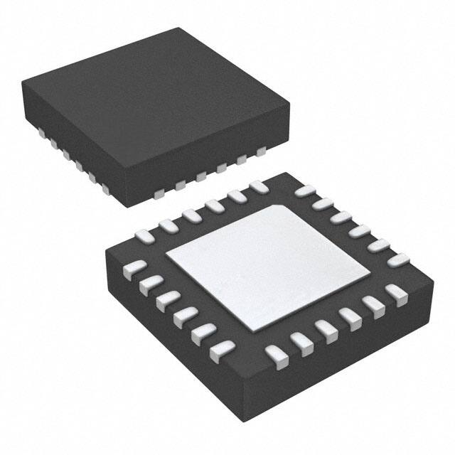


 工商网监
湘ICP备2023018690号
工商网监
湘ICP备2023018690号
