EVALUATION KIT AVAILABLE
Click here for production status of specific part numbers.
MAX2852
General Description
The MAX2852 is a single-chip RF receiver IC designed
for 5GHz wireless applications. The IC includes all circuitry required to implement a complete receiver-crystal
oscillator, VCO, PLL, LNA, VGA, and baseband filters. It
includes a fast-settling, sigma-delta fractional synthesizer
with 76Hz frequency programming step size. The IC also
integrates on-chip I/Q amplitude and phase-error calibration circuits. The receiver includes both an in-channel
RSSI and an RF RSSI.
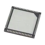
The receiver chip is housed in a small, 68-pin thin QFN
leadless plastic package with exposed pad.
Applications
●● 5GHz Wireless HDMI® (WHDI)
●● 5GHz FDD Backhaul and WiMAX™
5GHz Receiver
Features
●● 4900MHz to 5900MHz Frequency Range
●● 4.5dB Rx Noise Figure
●● 70dB Rx Gain-Control Range with 2dB Step Size,
Digitally Controlled
●● 60dB Dynamic Range Receiver RSSI
●● RF Wideband Receiver RSSI
●● Programmable 20MHz/40MHz Rx I/Q Lowpass
Channel Filters
●● Sigma-Delta Fractional-N PLL with 76Hz Resolution
●● Monolithic Low-Noise VCO with -35dBc
Integrated Phase Noise
●● 4-Wire SPI Digital Interface
●● I/Q Analog Baseband Interface
●● On-Chip Digital Temperature Sensor Readout
●● Complete Baseband Interface
●● +2.7V to +3.6V Supply Voltage
●● Small, 68-Pin Thin QFN Package (10mm x 10mm)
Ordering Information
PART
TEMP RANGE
PIN-PACKAGE
MAX2852ITK+
-25°C to +85°C
68 Thin QFN-EP*
*EP = Exposed pad.
+ Denotes a lead(Pb)-free/RoHS-compliant package.
HDMI is a registered trademark of HDMI Licensing, LLC.
WiMAX is a trademark of WiMAX Forum.
19-5010; Rev 3; 8/18
Typical Operating Circuit appears at end of data sheet.
�MAX2852
5GHz Receiver
Absolute Maximum Ratings
VCC_ Pins to GND................................................-0.3V to +3.9V
RF Inputs Maximum Current: RXRF+, RXRF
to GND............................................................... -1mA to +1mA
Analog Inputs: XTAL to GND................................-0.3V to +3.9V
Analog Outputs: RXBBI+, RXBBI-, RXBBQ+,
RXBBQ-, RSSI, CLKOUT2, VCOBYP, CPOUT+,
CPOUT- to GND................................................-0.3V to +3.9V
Digital Inputs: ENABLE, CS, SCLK, DIN to GND......-0.3V to +3.9V
Digital Outputs: DOUT, CLKOUT to GND.............-0.3V to +3.9V
Short-Circuit Duration
Analog Outputs................................................................... 10s
Digital Outputs.................................................................... 10s
RF Input Power...............................................................+10dBm
Continuous Power Dissipation (TA = +85°C)
68-Pin Thin QFN (derate 29.4mW/°C above +70°C).....2352mW
Operating Temperature Range............................ -25°C to +85°C
Junction Temperature.......................................................+150°C
Storage Temperature Range............................. -65°C to +160°C
Lead Temperature (soldering, 10s).................................. +300°C
Soldering Temperature (reflow)........................................+260°C
Stresses beyond those listed under “Absolute Maximum Ratings” may cause permanent damage to the device. These are stress ratings only, and functional operation of the device at these
or any other conditions beyond those indicated in the operational sections of the specifications is not implied. Exposure to absolute maximum rating conditions for extended periods may affect
device reliability.
CAUTION! ESD SENSITIVE DEVICE
DC Electrical Characteristics
(Operating conditions, unless otherwise specified: VCC = 2.7V~3.6V, ENABLE set according to operating mode, CS = high, SCLK =
DIN = low, TA = -25°C to +85°C. Typical values measured at VCC = 2.85V, LO frequency = 5.35GHz, TA = +25°C. Channel bandwidth
is set to 40MHz.) (Note 1)
PARAMETER
CONDITIONS
Supply Voltage, VCC
Supply Current
MIN
TYP
2.7
MAX
3.6
Shutdown mode, TA = +25°C
10
Clock-out only mode
7.4
11
60
89
Receive mode
135
174
Receive calibration mode
268
327
1.1
1.3
0.9
V
µA
Standby mode
Rx I/Q Output Common-Mode
Voltage
UNITS
mA
V
LOGIC INPUTS: ENABLE, SCLK, DIN, CS
Digital Input-Voltage High, VIH
VCC - 0.4
V
Digital Input-Voltage Low, VIL
0.4
V
Digital Input-Current High, IIH
-1
+1
µA
Digital Input-Current Low, IIL
-1
+1
µA
LOGIC OUTPUTS: DOUT, CLKOUT
Digital Output-Voltage High, VOH
Sourcing 1mA
Digital Output-Voltage Low, VOL
Sinking 1mA
Digital Output Voltage in
Shutdown Mode
Sinking 1mA
www.maximintegrated.com
VCC - 0.4
V
0.4
VOL
V
V
Maxim Integrated │ 2
�MAX2852
5GHz Receiver
AC Electrical Characteristics—Rx Mode
(Operating conditions, unless otherwise specified: VCC = 2.7V~3.6V, RF frequency = 5.351GHz, TA = -25°C to +85°C. LO frequency =
5.35GHz. Reference frequency = 40MHz, ENABLE = high, CS = high, SCLK = DIN = low, with power matching at RXRF+ and RXRFdifferential ports using the Typical Operating Circuit. Receiver I/Q output at 100mVRMS loaded with 10kΩ differential load resistance
and 10pF load capacitance. The RSSI pin is loaded with 10kΩ load resistance to ground. Typical values measured at VCC = 2.85V,
channel bandwidths of 40MHz, TA = +25°C.) (Note 1)
PARAMETER
CONDITIONS
MIN
TYP
MAX
UNITS
RECEIVER SECTION: RF INPUT TO I/Q BASEBAND LOADED OUTPUT (Includes 50Ω to 100 Ω RF Balun and Matching)
RF Input Frequency Range
4.9
5.9
Peak-to-Peak Gain Variation
4.9GHz to 5.35GHz
over RF Frequency Range at One
5.35GHz to 5.9GHz
Temperature
0.3
2.6
2.2
5.3
RF Input Return Loss
-6
Total Voltage Gain
RF Gain Steps Relative to
Maximum Gain
Baseband Gain Range
All LNA settings
Maximum gain; Main address 1 D7:0 = 11111111
61
-2
Main address 1 D7:D5 = 110
-8
Main address 1 D7:D5 = 101
-16
Main address 1 D7:D5 = 001
-32
Main address 1 D7:D5 = 000
-40
From maximum baseband gain (Main address 1 D3:D0 =
1111) to minimum baseband gain (Main address 1 D3:D0
= 0000)
Baseband Gain Step
27.5
30
dB
dB
68
Minimum gain; Main address 1 D7:0 = 00000000
GHz
+5.0
dB
dB
32.5
dB
2
dB
RF Gain-Change Settling Time
Gain settling to within ±0.5dB of steady state; RXHP = 1
400
ns
Baseband Gain-Change Settling
Time
Gain settling to within ±0.5dB of steady state; RXHP = 1
200
ns
DSB Noise Figure
www.maximintegrated.com
Balun input referred,
integrated from 10kHz
to 9.5MHz at I/Q
baseband output for
20MHz RF bandwidth
Maximum RF gain (Main
address 1 D7:D5 = 111)
4.5
Maximum RF gain - 16dB
(Main address 1 D7:D5 = 101)
15
Balun input referred,
integrated from 10kHz
to 19MHz at I/Q
baseband output for
40MHz RF bandwidth
Maximum RF gain (Main
address 1 D7:D5 = 111)
4.5
Maximum RF gain - 16dB
(Main address 1 D7:D5 = 101)
15
dB
Maxim Integrated │ 3
�MAX2852
5GHz Receiver
AC Electrical Characteristics—Rx Mode (continued)
(Operating conditions, unless otherwise specified: VCC = 2.7V~3.6V, RF frequency = 5.351GHz, TA = -25°C to +85°C. LO frequency =
5.35GHz. Reference frequency = 40MHz, ENABLE = high, CS = high, SCLK = DIN = low, with power matching at RXRF+ and RXRFdifferential ports using the Typical Operating Circuit. Receiver I/Q output at 100mVRMS loaded with 10kΩ differential load resistance
and 10pF load capacitance. The RSSI pin is loaded with 10kΩ load resistance to ground. Typical values measured at VCC = 2.85V,
channel bandwidths of 40MHz, TA = +25°C.) (Note 1)
PARAMETER
CONDITIONS
20MHz RF channel;
two-tone jammers at
+25MHz and +48MHz
frequency offset with
-39dBm/tone
Out-of-Band Input IP3
40MHz RF channel;
two-tone jammers at
+50MHz and +96MHz
frequency offset with
-39dBm/tone
1dB Gain Desensitization by
Alternate Channel Blocker
Input 1dB Gain Compression
MIN
TYP
-65dBm wanted signal; RF gain
= max (Main address 1 D7:D0
= 11101001)
-13
-49dBm wanted signal; RF gain
= max - 16dB (Main address 1
D7:D0 = 10101001)
-5
-45dBm wanted signal; RF gain
= max - 32dB (Main address 1
D7:D0 = 00111111)
11
-65dBm wanted signal; RF gain
= max (Main address 1 D7:D0
= 11101001)
-13
-49dBm wanted signal; RF gain
= max - 16dB (Main address 1
D7:D0 = 10101001)
-5
-45dBm wanted signal; RF gain
= max - 32dB (Main address 1
D7:D0 = 00101001)
11
Blocker at ±40MHz offset frequency for 20MHz RF
channel
-24
Blocker at ±80MHz offset frequency for 40MHz RF
channel
-24
Max RF gain (Main address 1 D7:D5 = 111)
-32
Max RF gain - 8dB (Main address 1 D7:D5 = 110)
-24
Max RF gain - 16dB (Main address 1 D7:D5 = 101)
-16
Max RF gain - 32dB (Main address 1 D7:D5 = 001)
0
dBm
0.63
Baseband -3dB Lowpass Corner
Frequency
Main address 0 D1 = 0
9.5
Main address 0 D1 = 1
19
Baseband Filter Stopband
Rejection
Rejection at 30MHz offset frequency for 20MHz channel
57
70
Rejection at 60MHz offset frequency for 40MHz channel
57
70
Baseband -3dB Highpass Corner
Frequency
Main address 5 D1 = 1
600
Main address 5 D1 = 0
10
www.maximintegrated.com
UNITS
dBm
Over passband frequency range; at any gain setting; 1dB
compression point
Output 1dB Gain Compression
MAX
dBm
VP-P
MHz
dB
kHz
Maxim Integrated │ 4
�MAX2852
5GHz Receiver
AC Electrical Characteristics—Rx Mode (continued)
(Operating conditions, unless otherwise specified: VCC = 2.7V~3.6V, RF frequency = 5.351GHz, TA = -25°C to +85°C. LO frequency =
5.35GHz. Reference frequency = 40MHz, ENABLE = high, CS = high, SCLK = DIN = low, with power matching at RXRF+ and RXRFdifferential ports using the Typical Operating Circuit. Receiver I/Q output at 100mVRMS loaded with 10kΩ differential load resistance
and 10pF load capacitance. The RSSI pin is loaded with 10kΩ load resistance to ground. Typical values measured at VCC = 2.85V,
channel bandwidths of 40MHz, TA = +25°C.) (Note 1)
PARAMETER
CONDITIONS
MIN
TYP
MAX
UNITS
Steady-State I/Q Output DC Error
with AC-Coupling
50µs after enabling receive mode and toggling RxHP
from 1 to 0, averaged over many measurements if I/Q
noise voltage exceeds 1mVRMS, at any given gain
setting, no input signal, 1-sigma value
I/Q Gain Imbalance
1MHz baseband output, 1-sigma value
0.1
dB
I/Q Phase Imbalance
1MHz baseband output, 1-sigma value
0.2
degrees
Sideband Suppression
1MHz baseband output (Note 2)
40
dB
LO frequency
-75
2 x LO frequency
-62
3 x LO frequency
-75
Receiver Spurious Signal
Emissions
RF RSSI Output Voltage
Baseband RSSI Slope
2
4 x LO frequency
-60
-20dBm input power
1.75
19.5
26.5
mV
dBm/
MHz
V
35.5
mV/dB
Baseband RSSI Maximum Output
Voltage
2.3
V
Baseband RSSI Minimum Output
Voltage
0.5
V
www.maximintegrated.com
Maxim Integrated │ 5
�MAX2852
5GHz Receiver
AC Electrical Characteristics—Frequency Synthesis
(Operating conditions, unless otherwise specified: VCC = 2.7V~3.6V, frequency = 5.35GHz, TA = -25°C to +85°C. Reference frequency
= 40MHz, ENABLE = high, CS = high, SCLK = DIN = low. Typical values measured at VCC = 2.85V, TA = +25°C, LO frequency =
5.35GHz, TA = +25°C.) (Note 1)
PARAMETER
CONDITIONS
MIN
TYP
MAX
UNITS
5.9
GHz
FREQUENCY SYNTHESIZER
RF Channel Center Frequency
4.9
Channel Center Frequency
Programming Step
Closed-Loop Integrated Phase
Noise
Loop BW = 200kHz, integrate phase noise from 1kHz to
10MHz
Charge-Pump Output Current
Spur Level
Hz
-35
dBc
0.8
mA
fOFFSET = 0 to 19MHz
-42
fOFFSET = 40MHz
-66
Reference Frequency
dBc
40
Reference Frequency Input
Levels
AC-coupled to XTAL pin
800
CLKOUT Signal Level
10pF load capacitance
VCC 0.8
www.maximintegrated.com
76.294
MHz
mVP-P
VCC 0.1
VP-P
Maxim Integrated │ 6
�MAX2852
5GHz Receiver
AC Electrical Characteristics—Miscellaneous Blocks
(Operating conditions, unless otherwise specified: VCC = 2.7V~3.6V, TA = -25°C to +85°C. Reference frequency = 40MHz, ENABLE
= high, CS = high, SCLK = DIN = low. Typical values measured at VCC = 2.85V, TA = +25°C.) (Note 1)
PARAMETER
CONDITIONS
MIN
TYP
MAX
UNITS
ON-CHIP TEMPERATURE SENSOR
Digital Output Code
Read-out at DOUT pin through
Main address 3 D4:D0
TA = +25°C
17
TA = +85°C
25
TA = -20°C
9
AC Electrical Characteristics—Timing
(Operating conditions, unless otherwise specified: VCC = 2.7V~3.6V, frequency = 5.35GHz, TA = -25°C to +85°C. Reference frequency
= 40MHz, ENABLE = high, CS = high, SCLK = DIN = low. Typical values measured at VCC = 2.85V, TA = +25°C, LO frequency =
5.35GHz, TA = +25°C.) (Note 1)
PARAMETER
SYMBOL
CONDITIONS
MIN
TYP
MAX
UNITS
SYSTEM TIMING
Shutdown Time
2
µs
Maximum Channel Switching
Time
Loop bandwidth = 200kHz, settling to within
±1kHz from steady state
2
ms
Maximum Channel Switching
Time With Preselected VCO
Sub-Band
Loop bandwidth = 200kHz, settling to within
±1kHz from steady state
56
µs
Rx Turn-On Time (from
Standby Mode)
Measured from CS rising edge, Rx gain settles
to within 0.5dB of steady state
2
µs
Rx Turn-Off Time (to Standby
Mode)
From CS rising edge
0.1
µs
4-WIRE SERIAL-INTERFACE TIMING (See Figure 1)
SCLK Rising Edge to CS
Falling Edge Wait Time
tCSO
6
ns
Falling Edge of CS to Rising
Edge of First SCLK Time
tCSS
6
ns
DIN to SCLK Setup Time
tDS
6
ns
DIN to SCLK Hold Time
tDH
6
ns
www.maximintegrated.com
Maxim Integrated │ 7
�MAX2852
5GHz Receiver
AC Electrical Characteristics—Timing (continued)
(Operating conditions, unless otherwise specified: VCC = 2.7V~3.6V, frequency = 5.35GHz, TA = -25°C to +85°C. Reference frequency
= 40MHz, ENABLE = high, CS = high, SCLK = DIN = low. Typical values measured at VCC = 2.85V, TA = +25°C, LO frequency =
5.35GHz, TA = +25°C.) (Note 1)
PARAMETER
SYMBOL
CONDITIONS
MIN
TYP
MAX
UNITS
SCLK Pulse-Width High
tCH
6
ns
SCLK Pulse-Width Low
tCL
6
ns
Last Rising Edge of SCLK to
Rising Edge of CS or Clock to
Load Enable Setup Time
tCSH
6
ns
CS High Pulse Width
tCSW
50
ns
Time Between Rising Edge of
CS and the Next Rising Edge
of SCLK
tCS1
6
ns
SCLK Frequency
fCLK
40
MHz
Rise Time
tR
2.5
ns
Fall Time
tF
2.5
ns
SCLK Falling Edge to Valid
DOUT
tD
12.5
ns
Note 1: The MAX2852 is production tested at TA = +25°C; minimum/maximum limits at TA = +25°C are guaranteed by test, unless
specified otherwise. Minimum/maximum limits at TA = -25°C and +85°C are guaranteed by design and characterization. There
is no power-on register settings self-reset; recommended register settings must be loaded after VCC is applied.
Note 2: For optimal Rx quadrature accuracy over temperature, the user can utilize the Rx calibration circuit to assist quadrature calibration.
www.maximintegrated.com
Maxim Integrated │ 8
�MAX2852
5GHz Receiver
Typical Operating Characteristics
(VCC = 2.8V, fLO = 5.35GHz, fREF = 40MHz, CS = high, SCLK = DIN = low, RF BW = 20MHz, TA = +25°C, using the MAX2852 Evaluation Kit.)
137
TA = -20°C
TA = +25°C
25
MAX - 16dB
15
10
133
5
0
2.6 2.7 2.8 2.9 3.0 3.1 3.2 3.3 3.4 3.5 3.6
MAX - 24dB
20
134
MAX - 8dB
MAX
SUPPLY VOLTAGE (V)
TA = +25°C
65
5.3
5.5
40
30
LNA = MAX - 32dB
0
5.7
-10
5.9
LNA = MAX - 40dB
4.9
5.1
LNA = MAX - 24dB
LNA = MAX - 40dB
2
10
-70
-50
MAX2852 toc03
0.50
0.45
TA = +25°C
0.40
TA = +85°C
0.35
0.30
0.25
0.20
16
6
VGA GAIN =
3/5/7/9/11/13/15
-10
10
0
0
2
14
12
10
20MHz OFFSET
8
6
4
40MHz OFFSET
2
LNA = MAX = -32dB
-30
14
VGA GAIN = 0
8
2
INPUT POWER (dBm)
www.maximintegrated.com
VGA GAIN = 2/4/6/8/10/12/14
10
Rx EVM (%)
LNA = MAX = -16dB
LNA = MAX = -24dB
12
4
-35
14
TA = -20°C
Rx EVM vs. OFDM JAMMER POWER AT
20MHz AND 40MHz OFFSET FREQUENCY
WITH WANTED SIGNAL AT -66dBm
-30
12
Rx OUTPUT V1dB vs. GAIN SETTING
Rx EVM vs. Rx BASEBAND
OUTPUT LEVEL
LNA = MAX = -40dB
8
5.9
Rx EVM vs. INPUT POWER
(CHANNEL BANDWIDTH = 20MHz)
LNA = MAX = -8dB
6
5.7
4
8
10 12
6
BASEBAND VGA GAIN CODE
-25
4
5.5
BASEBAND VGA GAIN CODE
-20
0
5.3
FREQUENCY (GHz)
LNA = MAX
-90
30
MAX2852 toc09
5.1
-15
-40
LNA = MAX - 16dB
10
TA = +85°C
4.9
LNA = MAX - 32dB
0.55
Rx EVM (%)
62
LNA = MAX - 8dB
20
63
40
0.60
OUTPUT V1dB (VRMS)
GAIN (dB)
50
64
EVM (dB)
60
68
67
LNA = MAX
70
MAX2852 toc07
MAXIMUM GAIN (dB)
69
66
LNA = MAX - 24dB
FREQUENCY (GHz)
Rx GAIN vs. BASEBAND VGA GAIN
80
MAX2852 toc04
TA = -20°C
70
LNA = MAX - 16dB
50
Rx VGA GAIN SETTINGS
Rx MAXIMUM GAIN vs.
TEMPERATURE AND FREQUENCY
71
LNA = MAX - 8dB
60
20
0 1 2 3 4 5 6 7 8 9 10 11 12 13 14 15
MAX2852 toc08
132
MAX - 32dB
30
LNA = MAX GAIN
70
MAX2852 toc05
135
MAX - 40dB
35
MAX2852 toc06
138
136
40
Rx MAXIMUM GAIN vs. FREQUENCY
80
MAXIMUM GAIN (dB)
TA = +85°C
NOISE FIGURE (dB)
SUPPLY CURRENT (mA)
140
139
45
MAX2852 toc01
141
Rx NOISE FIGURE vs. VGA GAIN
SETTINGS (BALUN INPUT REFERRED)
MAX2852 toc02
Rx MODE SUPPLY CURRENT
-30
-25
-20
-15
-10
-5
Rx BASEBAND OUTPUT LEVEL (dBVrms)
0
0
-40 -35 -30 -25 -20 -15 -10 -5
0
5
10
INPUT POWER (dBm)
Maxim Integrated │ 9
�MAX2852
5GHz Receiver
Typical Operating Characteristics (continued)
(VCC = 2.8V, fLO = 5.35GHz, fREF = 40MHz, CS = high, SCLK = DIN = low, RF BW = 20MHz, TA = +25°C, using the MAX2852 Evaluation Kit.)
2LO
4LO
REAL PART (Ω)
(dBm)
-40
-50
-60
-70
-80
-90
MAX GAIN
30
20
0
MAX - 32dB
MAX - 40dB
10
-10
MAX GAIN
0
-20
MAX - 40dB
-10
-30
-100
0
2.65GHz/div
-20
5.20
5.40
5.60
5.80
-40
6.00
HIGH GAIN,
TA = +85°C
-14
LNA = MAX - 40dB
-16
-18
-20
4900
5100
5300
5500
0V
5700
5900
Rx RF RSSI DELAY TIME
(-40dB SIGNAL STEP)
MAX2852 toc15
∆: 216ns ∆: 1.30V
@: 128ns @: 460mV
1.0V/div
GAIN CONTROL
0V
1.0V/div
1.0V/div
HIGH GAIN,
TA = +25°C
0.5
LNA = MAX - 32dB
-12
∆: 280ns ∆: 1.32V
@: 192ns @: 1.84V
0V
1.0
-10
FREQUENCY (MHz)
1.0V/div
LOW GAIN,
TA = -20°C
LNA = MAX
-8
MAX2852 toc14
LOW GAIN,
TA = +25°C
1.5
5.00
-6
Rx RF RSSI ATTACK TIME
(+40dB SIGNAL STEP)
LOW GAIN, TA = +85°C
2.0
4.80
-4
RF FREQUENCY (GHz)
Rx RF RSSI OUTPUT
2.5
RF RSSI OUTPUT VOLTAGE (V)
26.5
MAX2852 toc13
-110
-2
10
20
Rx INPUT RETURN LOSS
0
MAX2852 toc12
-30
MAX - 32dB
MAX2852 toc11
Rx INPUT RETURN LOSS (dB)
-20
Rx INPUT IMPEDANCE
40
MAX2852 toc10
-10
IMAGINARY PART (Ω)
Rx EMISSION SPECTRUM AT
LNA INPUT (LNA = MAX GAIN)
VRSSI
GAIN CONTROL
VRSSI
0V
HIGH GAIN, TA = -20°C
0
-50 -45 -40 -35 -30 -25 -20 -15 -10 -5
0
400ns/div
400ns/div
Rx BASEBAND RSSI
+40dB STEP RESPONSE
Rx BASEBAND RSSI
-32dB STEP RESPONSE
RF INPUT POWER (dBm)
BASEBAND RSSI VOLTAGE
vs. INPUT POWER
MAX2852 toc17
MAX2852 toc16
BASEBAND RSSI OUTPUT VOLTAGE (V)
3.0
LNA = MAX LNA = MAX - 40dB
2.5
LNA = MAX - 8dB
2.0
1.0
LNA GAIN CONTROL
RSSI OUTPUT
0V
2.0V
0.6V
LNA GAIN CONTROL
RSSI OUTPUT
LNA = MAX - 32dB
0.5
0
0.8V
LNA =
MAX - 24dB
2.7V
2.7V
0V
2.4V
1.5
MAX2852 toc18
∆: 1.18µs D: 1.62V
@: 1.16µs @: 480mV
∆: 460ns ∆: 1.50V
@: 440ns @: 2.30V
LNA = MAX - 16dB
-100
-80
-60
-40
-20
0
20
1µs/div
1µs/div
RF INPUT POWER (dBm)
www.maximintegrated.com
Maxim Integrated │ 10
�MAX2852
5GHz Receiver
Typical Operating Characteristics (continued)
(VCC = 2.8V, fLO = 5.35GHz, fREF = 40MHz, CS = high, SCLK = DIN = low, RF BW = 20MHz, TA = +25°C, using the MAX2852 Evaluation Kit.)
RESPONSE (dB)
RESPONSE (dB)
Rx LPF 20MHz CHANNEL
BANDWIDTH GROUP DELAY
-135
10k
100M
-135
10k
BASEBAND FREQUENCY (Hz)
100M
Rx DC OFFSET SETTLING RESPONSE
(-30dB Rx VGA GAIN STEP)
GROUP DELAY (ns)
0V
Rx BASEBAND
I/Q OUTPUT
50mV/div
10k
FREQUENCY (Hz)
0V
GAIN-CONTROL
TOGGLE
10mV/div
Rx BASEBAND
I/Q OUTPUT
GAIN-CONTROL TOGGLE
0V
Rx BASEBAND
I/Q OUTPUT
10mV/div
Rx BASEBAND
I/Q OUTPUT
www.maximintegrated.com
Rx BASEBAND DC OFFSET SETTLING
RESPONSE WITH RxHP = 1
(MAX - 40dB TO MAX LNA GAIN STEP)
MAX2852 toc27
CH1 PEAK TO
PEAK: 69.0mV
Rx BASEBAND
I/Q OUTPUT
0V
10mV/div
50mV/div
200ns/div
200ns/div
MAX2852 toc26
MAX2852 toc25
100M
CH1 PEAK TO
PEAK: 8.60mV
0V GAIN-CONTROL
TOGGLE
Rx DC OFFSET SETTLING RESPONSE
(+32dB Rx VGA GAIN STEP)
Rx DC OFFSET SETTLING RESPONSE
(+16dB Rx VGA GAIN STEP)
FREQUENCY (Hz)
MAX2852 toc24
200ns/div
100M
CH1 PEAK TO
PEAK: 17.3mV
CH1 PEAK TO
PEAK: 81.9mV
10k
Rx DC OFFSET SETTLING RESPONSE
(+8dB Rx VGA GAIN STEP)
MAX2852 toc23
MAX2852 toc22
GAIN-CONTROL
TOGGLE
0
0
FREQUENCY (Hz)
Rx LPF 40MHz CHANNEL
BANDWIDTH GROUP DELAY
100
MAX2852 toc21
100
GROUP DELAY (ns)
-35
MAX2852 toc19
-35
Rx LPF 40MHz CHANNEL BANDWIDTH
RESPONSE
MAX2852 toc20
Rx LPF 20MHz CHANNEL BANDWIDTH
RESPONSE
200ns/div
GAIN-CONTROL
TOGGLE
10µs/div
Maxim Integrated │ 11
�MAX2852
5GHz Receiver
Typical Operating Characteristics (continued)
(VCC = 2.8V, fLO = 5.35GHz, fREF = 40MHz, CS = high, SCLK = DIN = low, RF BW = 20MHz, TA = +25°C, using the MAX2852 Evaluation Kit.)
Rx BASEBAND DC OFFSET SETTLING
RESPONSE WITH RxHP = 0
(MAX TO MAX - 40dB LNA GAIN STEP)
MAX2852 toc28
Rx BASEBAND
I/Q OUTPUT
0V
50mV/div
MAX2852 toc30
MAX2852 toc29
GAIN-CONTROL
TOGGLE
GAIN-CONTROL
TOGGLE
Rx BASEBAND
I/Q OUTPUT
0V
Rx BASEBAND
I/Q OUTPUT
0V
10mV/div
GAIN-CONTROL
TOGGLE
50mV/div
10µs/div
10µs/div
10µs/div
Rx BASEBAND VGA SETTLING
RESPONSE (-30dB BASEBAND
VGA GAIN STEP)
Rx BASEBAND VGA SETTLING
RESPONSE (+4dB BASEBAND
VGA GAIN STEP)
Rx BASEBAND VGA SETTLING
RESPONSE (+16dB BASEBAND
VGA GAIN STEP)
MAX2852 toc31
MAX2852 toc32
GAIN-CONTROL
TOGGLE
Rx BASEBAND
I/Q OUTPUT
0V
0.1V/div
MAX2852 toc33
CH1 PEAK TO
PEAK: 568mV
GAIN-CONTROL
TOGGLE
CH1 PEAK TO
PEAK : 652mV
CH1 PEAK TO
PEAK: 532mV
Rx BASEBAND
OUTPUT
0V
Rx BASEBAND
OUTPUT
0V
0.1V/div
0.1V/div
GAIN-CONTROL
TOGGLE
100ns/div
100ns/div
100ns/div
Rx BASEBAND VGA SETTLING
RESPONSE (+30dB BASEBAND
VGA GAIN STEP)
Rx LNA SETTLING RESPONSE
(MAX TO MAX - 40dB GAIN STEP)
Rx LNA SETTLING RESPONSE
(MAX - 8dB TO MAX GAIN STEP)
MAX2852 toc34
MAX2852 toc35
GAIN-CONTROL
TOGGLE
0V
0.1V/div
MAX2852 toc36
∆: 130mv
@: 132mv
CH1 PEAK TO
PEAK: 800mV
CLIPPING NEGATIVE
Rx BASEBAND
OUTPUT
0V
Rx BASEBAND DC OFFSET SETTLING
RESPONSE WITH RxHP = 0
(MAX - 40dB TO MAX LNA GAIN STEP)
Rx BASEBAND DC OFFSET SETTLING
RESPONSE WITH RxHP = 1
(MAX - 40dB TO MAX LNA GAIN STEP)
CH1 RMS:
168mV
GAIN-CONTROL
TOGGLE
0.1V/div
GAIN-CONTROL
TOGGLE
Rx BASEBAND
OUTPUT
0V
0.1V/div
Rx BASEBAND
OUTPUT
∆: 130mv
@: 132mv
CH1 RMS:
188mV
100ns/div
www.maximintegrated.com
100ns/div
100ns/div
Maxim Integrated │ 12
�MAX2852
5GHz Receiver
Typical Operating Characteristics (continued)
(VCC = 2.8V, fLO = 5.35GHz, fREF = 40MHz, CS = high, SCLK = DIN = low, RF BW = 20MHz, TA = +25°C, using the MAX2852 Evaluation Kit.)
Rx LNA SETTLING RESPONSE
(MAX - 16dB TO MAX GAIN STEP)
Rx LNA SETTLING RESPONSE
(MAX - 24dB TO MAX GAIN STEP)
Rx LNA SETTLING RESPONSE
(MAX - 32dB TO MAX GAIN STEP)
CH1 RMS: 176mV
CH1 RMS: 174mV
CH1 RMS: 155mV
MAX2852 toc37
Rx BASEBAND
OUTPUT
GAIN-CONTROL
TOGGLE
MAX2852 toc39
MAX2852 toc38
Rx BASEBAND
OUTPUT
GAIN-CONTROL
TOGGLE
Rx BASEBAND
OUTPUT
0V
0V
0V
0.1V/div
0.1V/div
0.1V/div
∆: 130mv
@: 132mv
∆: 130mv
@: 132mv
100ns/div
∆: 130mv
@: 132mv
200ns/div
100ns/div
Rx LNA SETTLING RESPONSE
(MAX - 40dB TO MAX GAIN STEP)
MAX2852 toc40
CH1 RMS: 154mV
Rx BASEBAND
OUTPUT
GAIN-CONTROL
TOGGLE
0V
0.1V/div
∆: 130mv
@: 132mv
HISTOGRAM: Rx I/Q GAIN IMBALANCE
MAX2852 toc41
648
HISTOGRAM: Rx I/Q PHASE IMBALANCE
150
432
120
324
90
216
60
108
30
0
-800.00m
200ns/div
HISTOGRAM: Rx STATIC DC OFFSET
MAX2852 toc43
800.00m
0
POWER-ON DC OFFSET CANCELLATION
WITH INPUT SIGNAL
POWER-ON DC OFFSET CANCELLATION
WITHOUT INPUT SIGNAL
110
66
Rx ENABLE
Rx BASEBAND OUTPUT
MAX2852 toc45
22
Rx ENABLE
RXBB_I
50mV/div
RXBB_Q
TURN-ON
TRANSIENT
500mV/div
0V
0.1V/div
44
2.0000
SAMPLES = 3413, AVG = -0.015deg, STDEV = 0.042dB
MAX2852 toc44
0V
2V/div
0
-2.0000
SAMPLES = 3413, AVG = -0.015dB, STDEV = 0.042dB
∆: 2.14µs ∆: 112mV
@: 2.12µs @: 104mV
88
MAX2852 toc42
180
540
0
132
GAIN-CONTROL
TOGGLE
ENGAGE 600kHz
HIGHPASS CORNER
0
-15.0000
0
15.0000
1µs/div
400ns/div
SAMPLES = 3413, AVG = -0.5mV, STDEV = 2.14mV
www.maximintegrated.com
Maxim Integrated │ 13
�MAX2852
5GHz Receiver
Typical Operating Characteristics (continued)
(VCC = 2.8V, fLO = 5.35GHz, fREF = 40MHz, CS = high, SCLK = DIN = low, RF BW = 20MHz, TA = +25°C, using the MAX2852 Evaluation Kit.)
5.5
5.0
400
300
200
4.5
100
4.0
0
0
0.5
1.0
1.5
2.0
2.5
0
0.5
1.0
1.5
2.0
-90
-100
-110
-120
-150
2.5
-90
-100
-110
-120
10M
CHANNEL SWITCHING FREQUENCY
SETTLING (4900MHz TO 5900MHz,
AUTOMATIC VCO SUB-BAND SELECTION)
25kHz
CHANNEL SWITCHING FREQUENCY
SETTLING (5900MHz TO 4900MHz,
AUTOMATIC VCO SUB-BAND SELECTION)
FREQUENCY (5kHz/div)
-80
1k
OFFSET FREQUENCY (Hz)
MAX2852 toc50
MAX2852 toc49
25kHz
MAX2852 toc48
-80
-140
FREQUENCY (5kHz/div)
PHASE NOISE (dBc/Hz)
-70
-70
DIFFERENTIAL TUNE VOLTAGE (V)
LO PHASE NOISE AT 5900MHz AND HOT
TEMPERATURE
-60
-60
-130
DIFFERENTIAL TUNE VOLTAGE (V)
-50
-50
PHASE NOISE (dBc/Hz)
500
LO GAIN (MHz/V)
6.0
LO PHASE NOISE AT 5350MHz AND ROOM
TEMPERATURE
MAX2852 toc47
6.5
LO FREQUENCY (GHz)
600
MAX2852 toc46
7.0
LO GAIN vs. DIFFERENTIAL
TUNE VOLTAGE AT TA = +25°C
MAX2852 toc51
LO FREQUENCY vs. DIFFERENTIAL
TUNE VOLTAGE AT TA = +25°C
-130
-140
1k
10M
-25kHz
0s
OFFSET FREQUENCY (Hz)
-25kHz
400µs/div
25kHz
-25kHz
0s
3.99ms
400µs/div
CHANNEL SWITCHING FREQUENCY
SETTLING (5900MHz TO 4900MHz,
MANUAL VCO SUB-BAND SELECTION)
FREQUENCY (5kHz/div)
MAX2852 toc52
FREQUENCY (5kHz/div)
25kHz
CHANNEL SWITCHING FREQUENCY
SETTLING (4900MHz TO 5900MHz,
MANUAL VCO SUB-BAND SELECTION)
3.99ms
MAX2852 toc53
-150
0s
99.22µs
10µs/div
www.maximintegrated.com
-25kHz
0s
99.22µs
10µs/div
Maxim Integrated │ 14
�MAX2852
5GHz Receiver
N.C.
N.C.
N.C.
RXBBI+
N.C.
RXBBQ+
RXBBI-
RXBBQ-
RSSI
V CC_VCO
GND_VCO
CPOUT+
CPOUT-
V CC_DIG
CLKOUT
DOUT
TOP VIEW
BYP_VCO
Pin Configuration
51 50 49 48 47 46 45 44 43 42 41 40 39 38 37 36 35
V CC_XTAL 52
34 DIN
XTAL 53
33 SCLK
32 CS
XTAL_CAP 54
ENABLE 55
31 N.C.
N.C. 56
30 N.C.
N.C. 57
29 N.C.
N.C. 58
28 N.C.
MAX2852
N.C. 59
27 V CC_BB2
26 V CC_MXR
V CC_BB1 60
N.C. 61
25 RXRF+
N.C. 62
24 RXRF-
N.C. 63
23 V CC_LNA
N.C. 64
22 N.C.
N.C. 65
21 V CC
V CC 66
20 V CC
V CC 67
19 N.C.
N.C. 68
V CC
N.C.
GND
V CC
V CC
GND
N.C.
V CC
10 11 12 13 14 15 16 17
V CC
9
V CC
8
GND
7
N.C.
6
V CC
5
V CC
4
N.C.
3
V CC
2
V CC
18 GND
1
TQFN
10mm x 10mm
www.maximintegrated.com
Maxim Integrated │ 15
�MAX2852
5GHz Receiver
Pin Description
PIN
NAME
1, 2, 5, 6, 9,
10, 12, 13, 16,
17, 20, 21,
66, 67
FUNCTION
VCC
Supply Voltage
3, 8, 11, 14,
19, 22, 28–31,
35–38, 56–59,
61–65, 68
N.C.
No Connection
4, 7, 15, 18
GND
Ground
23
VCC_LNA
Receiver LNA Supply Voltage. Bypass with a capacitor as close as possible to the pin.
24
RXRF-
25
RXRF+
26
VCC_MXR
Receiver Downconverter Supply Voltage. Bypass with a capacitor as close as possible to the pin.
27
VCC_BB2
Receiver Baseband Supply Voltage 2. Bypass with a capacitor as close as possible to the pin.
32
CS
Chip-Select Logic Input of 4-Wire Serial Interface
33
SCLK
Serial-Clock Logic Input of 4-Wire Serial Interface
34
DIN
39
RXBBI+
40
RXBBI-
41
RXBBQ+
42
RXBBQ-
43
RSSI
44
VCC_VCO
VCO Supply Voltage. Bypass with a capacitor as close as possible to the pin.
45
BYP_VCO
On-Chip VCO Regulator Output Bypass. Bypass with an external 1µF capacitor to GND_VCO with
minimum PCB trace. Do not connect other circuitry to this pin.
46
GND_VCO
VCO Ground
47
CPOUT+
48
CPOUT-
Differential Charge-Pump Outputs. Connect the frequency synthesizer’s loop filter between
CPOUT+ and CPOUT- (see the Typical Operating Circuit).
49
VCC_DIG
Digital Block Supply Voltage. Bypass with a capacitor as close as possible to the pin.
Receiver LNA Differential Inputs. Inputs are DC-coupled and biased internally at 1.2V.
Data Logic Input of 4-Wire Serial Interface
Receiver Baseband I-Channel Differential Outputs
Receiver Baseband Q-Channel Differential Outputs
Receiver Signal Strength Indicator Output
50
DOUT
51
CLKOUT
Data Logic Output of 4-Wire Serial Interface
Reference Clock Buffer Output
52
VCC_XTAL
Crystal Oscillator Supply Voltage. Bypass with a capacitor as close as possible to the pin.
53
XTAL
54
XTAL_CAP
Crystal Oscillator Base Input. AC-couple crystal unit to this pin.
Crystal Oscillator Emitter Node
55
ENABLE
Enable Logic Input
60
VCC_BB1
Receiver Baseband Supply Voltage 1. Bypass with a capacitor as close as possible to the pin.
—
EP
Exposed Paddle. Connect to the ground plane with multiple vias for proper operation and heat
dissipation. Do not share with any other pin grounds and bypass capacitors’ ground.
www.maximintegrated.com
Maxim Integrated │ 16
�MAX2852
5GHz Receiver
Table 1. Operating Modes
MODE-CONTROL
LOGIC INPUTS
CIRCUIT BLOCK STATES
MODE
ENABLE PIN
SPI MAIN
ADDRESS 0,
D4:D2
Rx PATH
LO PATH
CLKOUT*
Calibration Sections
On
SHUTDOWN
0
XXX
Off
Off
Off
None
CLKOUT
1
000
Off
Off
On
None
STANDBY
1
001
Off
On
On
None
Rx
1
010
On
On
On
None
*CLKOUT signal is active independent of SPI, and is only dependent on the ENABLE pin.
Detailed Description
Modes of Operation
The modes of operation for the MAX2852 are shutdown,
clockout, standby, and receive. See Table 1 for a summary of the modes of operation. The logic input pin
ENABLE (pin 55) and SPI Main address 0 D4:D2 control
the various modes.
Shutdown Mode
The MAX2852 features a low-power shutdown mode. All
circuit blocks are powered down, except the 4-wire serial
bus and its internal programmable registers.
Clockout Mode
In clockout mode, only the crystal oscillator signal is
active at the CLKOUT pin. The rest of the receiver is
powered down.
Standby Mode
In standby mode, PLL, VCO, and LO generation are on.
Rx mode can be quickly enabled from this mode. Other
blocks may be selectively enabled in this mode.
Receive (Rx) Mode
In receive mode, all Rx circuit blocks are powered on and
active. Antenna signal is applied; RF is downconverted,
filtered, and buffered at Rx baseband I and Q outputs.
Power-On Sequence
Set the ENABLE pin to VCC for 2ms to start the crystal
oscillator. Program all SPI addresses according to recommended values. Set SPI Main address 0 D4:D2 from 000
to 001 to engage standby mode. To lock the LO frequency, the user can set SPI in order of Main address 15, Main
address 16, and then Main address 17 to trigger VCO
sub-band autoacquisition; the acquisition will take 2ms.
After the LO frequency is locked, set SPI Main address 0
www.maximintegrated.com
D4:D2 = 010 for Rx operating mode. Before engaging Rx
mode, set Main address 5 D1 = 1 to allow fast DC offset
settling. After engaging Rx mode and Rx baseband DC
offset settles, the user can set Main address 5 D1 = 0 to
complete Rx DC offset cancellation.
Programmable Registers and
4-Wire SPI Interface
The MAX2852 includes 60 programmable 16-bit registers.
The most significant bit (MSB) is the read/write selection
bit (R/W in Figure 1). The next 5 bits are register address
(A4:A0 in Figure 1). The 10 least significant bits (LSBs)
are register data (D9:D0 in Figure 1). Register data is
loaded through the 4-wire SPI/MICROWIRE™-compatible
serial interface. MSB of data at the DIN pin is shifted in
first and is framed by CS. When CS is low, the clock is
active, and input data is shifted at the rising edge of the
clock at SCLK pin. At the CS rising edge, the 10-bit data
bits are latched into the register selected by address bits.
See Figure 1. To support more than a 32-register address
using a 5-bit wide address word, the bit 0 of address 0 is
used to select whether the 5-bit address word is applied
to the main address or local address. The register values
are preserved in shutdown mode as long as the powersupply voltage is maintained. There is no power-on SPI
register self-reset functionality in the MAX2852, so the
user must program all register values after power-up.
During the read mode, register data selected by address
bits is shifted out to the DOUT pin at the falling edges of
the clock.
SPI Register Definition
(All values in the register summary table are typical numbers. The MAX2852 SPI does not have a power-on-default
self-reset feature; the user must program all SPI addresses
for normal operation. Prior to use of any untested settings,
contact the factory.)
Maxim Integrated │ 17
�MAX2852
5GHz Receiver
tCSW
CS
tCSO
tCSH
tCSS
tCS1
SCLK
tDS
DIN
(SPI WRITE)
DIN
(SPI READ)
tCH
tDH
tCL
R/W
A4
A0
D9
D0
DON’T CARE
R/W
A4
A0
D9
D0
DON’T CARE
tD
DOUT
(SPI READ)
DON’T CARE
D9
D0
DON’T CARE
Figure 1. 4-Wire SPI Serial-Interface Timing Diagram
Table 2. Register Summary
READ/WRITE AND ADDRESS
REGISTER
Main0_
D0
Main0
Main1
Main2
Main3
0
0
0
0
A4:A0
00000
00001
00010
00011
www.maximintegrated.com
WRITE (W)/
READ (R)
W/R
DATA
D9
RESERVED
D8
0
1
W/R
RESERVED
RESERVED
0
W/R
RESERVED
D6
D5
D4
RESERVED RESERVED RESERVED RESERVED
Default
Default
D7
0
0
0
1
0
1
W
RESERVED
RESERVED
R
RESERVED
RESERVED
Default
0
0
1
1
0
0
TS_EN
TS_TRIG
0
0
0
D1
D0
RFBW
M/L_SEL
1
0
RX_VGA
1
LNA_BAND
0
D2
MODE
LNA_GAIN
RESERVED RESERVED
Default
0
D3
1
1
1
RESERVED RESERVED
0
0
RESERVED RESERVED RESERVED
RESERVED
0
1
1
1
RESERVED
RESERVED
RESERVED
0
0
0
RESERVED
RESERVED
RESERVED
0
0
TS_READ
0
0
0
Maxim Integrated │ 18
�MAX2852
5GHz Receiver
Table 2. Register Summary (continued)
READ/WRITE AND ADDRESS
REGISTER
Main0_
D0
Main4
0
A4:A0
00100
WRITE (W)/
DATA
D9
D8
Reserved
1
1
W/R
RESERVED
READ (R)
D7
D6
0
0
RSSI_MUX_SEL
D5
D4
D3
0
1
1
RESERVED RESERVED RESERVED
D2
D1
D0
1
0
0
RESERVED
RXHP
RESERVED
Main5
0
00101
Default
0
0
0
0
0
0
0
0
0
0
Main6
0
00110
Reserved
1
1
1
1
1
0
0
0
0
1
Main7
0
00111
Reserved
0
0
0
0
1
0
0
1
0
0
Main8
0
01000
W/R
0
0
0
0
0
0
0
0
0
0
Main9
0
01001
Main10
0
01010
Main11
0
01011
Main13
0
01101
Main14
0
01110
Main15
0
01111
W/R
RESERVED
RESERVED
RESERVED
RESERVED
Default
0
0
0
0
0
0
1
1
1
1
Reserved
0
0
0
0
0
0
0
0
0
0
W/R
RESERVED
RESERVED
RESERVED
RESERVED
0
Main17
Main18
0
0
0
10000
10001
10010
RESERVED RESERVED RESERVED RESERVED RESERVED RESERVED
Default
0
0
0
1
1
0
1
1
0
Reserved
0
0
0
0
0
0
0
0
0
0
W/R
RESERVED
RESERVED
DOUT_SEL
RESERVED
Default
0
0
0
0
0
0
1
0
0
0
0
0
0
0
0
0
0
0
0
1
W/R
Default
Main16
RESERVED RESERVED RESERVED RESERVED RESERVED RESERVED
RESERVED RESERVED RESERVED RESERVED RESERVED RESERVED
1
VAS_
Default
0
0
W/R
Default
10011
1
1
0
10100
Main21
0
10101
Main22
0
Main23
0
Main24
0
0
0
1
0
0
0
SYN_CONFIG_F
0
0
0
0
0
RESERVED RESERVED
0
RESERVED
0
XTAL_TUNE
0
1
RESERVED
RELOCK_
SEL
Read
Main20
0
SYN_CONFIG_F
VAS_
0
1
W/R
Default
1
SYN_CONFIG_N
W/R
W/R
Main19
1
RESERVED
TRIG_EN
1
0
0
0
0
VAS_
0
VAS_SPI
MODE
VAS_ADC
VCO_BAND
Default
0
0
0
1
0
1
1
1
1
Reserved
0
1
1
1
1
0
1
0
1
0
RESERVED
RESERVED
RESERVED
Read
RESERVED RESERVED
DIE_ID
RESERVED RESERVED
Default
0
0
1
0
1
1
1
1
1
1
10110
Reserved
0
1
1
0
1
1
1
0
0
0
10111
Reserved
0
0
0
1
1
0
0
1
0
1
0
11000
Reserved
1
0
0
1
0
0
1
1
1
1
Main25
0
11001
Reserved
1
1
1
0
1
0
1
0
0
0
Main26
0
11010
Reserved
0
0
0
0
0
1
0
1
0
1
W/R
DIE_ID_
READ
RESERVED
RESERVED
RESERVED
Default
0
0
0
0
RESERVED
RESERVED
RESERVED
0
1
1
Main27
Main28
0
0
11011
11100
www.maximintegrated.com
W/R
Default
RESERVED RESERVED RESERVED
1
1
0
VAS_VCO_
READ
0
RESERVED RESERVED RESERVED RESERVED RESERVED
0
0
0
1
1
RESERVED RESERVED
0
0
RESERVED RESERVED
0
0
Maxim Integrated │ 19
�MAX2852
5GHz Receiver
Table 2. Register Summary (continued)
READ/WRITE AND ADDRESS
REGISTER
Main0_
D0
A4:A0
WRITE (W)/
READ (R)
DATA
D9
D8
D7
D6
D5
D4
D3
D2
D1
D0
Main29
0
11101
Reserved
0
0
0
0
0
0
0
0
0
0
Main30
0
11110
Reserved
0
0
0
0
0
0
0
0
0
0
Main31
0
11111
Reserved
0
0
0
0
0
0
0
0
0
0
Local1
1
00001
Reserved
0
0
0
0
0
0
0
0
0
0
Local2
1
00010
Reserved
0
0
0
0
0
0
0
0
0
0
Local3
1
00011
Reserved
0
0
0
0
0
0
0
0
0
0
Local4
1
00100
Reserved
1
1
1
0
0
0
0
0
0
0
Local5
1
00101
Reserved
0
0
0
0
0
0
0
0
0
0
Local6
1
00110
Reserved
0
0
0
0
0
0
0
0
0
0
Local7
1
00111
Reserved
0
0
0
0
0
0
0
0
0
0
Local8
1
01000
Reserved
0
1
1
0
1
0
1
0
1
0
Local9
1
01001
Reserved
0
1
0
0
0
1
0
1
0
0
Local10
1
01010
Reserved
1
1
0
1
0
1
0
1
0
0
Local11
1
01011
Reserved
0
0
0
1
1
1
0
0
1
1
Local12
1
01100
Reserved
0
0
0
0
0
0
0
0
0
0
Local13
1
01101
Reserved
0
0
0
0
0
0
0
0
0
0
Local14
1
01110
Reserved
0
0
0
0
0
0
0
0
0
0
Local15
1
01111
Reserved
0
0
0
0
0
0
0
0
0
0
Local16
1
10000
Reserved
0
0
0
0
0
0
0
0
0
0
Local17
1
10001
Reserved
0
0
0
0
0
0
0
0
0
0
Local18
1
10010
Reserved
0
0
0
0
0
0
0
0
0
0
Local19
1
10011
Reserved
0
0
0
0
0
0
0
0
0
0
Local20
1
10100
Reserved
0
0
0
0
0
0
0
0
0
0
Local21
1
10101
Reserved
0
0
0
0
0
0
0
0
0
0
Local22
1
10110
Reserved
0
0
0
0
0
0
0
0
0
0
Local23
1
10111
Reserved
0
0
0
0
0
0
0
0
0
0
Local24
1
11000
Reserved
0
0
1
1
0
0
0
1
0
0
Local25
1
11001
Reserved
0
1
0
0
1
0
1
0
1
1
Local26
1
11010
Reserved
0
1
0
1
1
0
0
1
0
1
Local27
1
11011
W/R
RESERVED
RESERVED
RESERVED
RESERVED
Default
0
0
0
0
0
0
0
0
0
0
Local28
1
11100
Reserved
0
0
0
0
0
0
0
1
0
0
Local31
1
11111
Reserved
0
0
0
0
0
0
0
0
0
0
www.maximintegrated.com
RESERVED RESERVED RESERVED RESERVED RESERVED RESERVED
Maxim Integrated │ 20
�MAX2852
5GHz Receiver
Table 3. Main Address 0: (A4:A0 = 00000)
BIT NAME
BIT LOCATION
(D0 = LSB)
RESERVED
D9:D5
Reserved bits; set to default
MODE
D4:D2
IC Operating Mode Select
000 = Clockout (default)
001 = Standby
010 = Rx
011 = Do not use
RFBW
D1
RF Bandwidth
0 = 20MHz
1 = 40MHz (default)
M/L_SEL
D0
Main or Local Address Select
0 = Main registers (default)
1 = Local registers
DESCRIPTION
Table 4. Main Address 1: (A4:A0 = 00001, Main Address 0 D0 = 0)
BIT NAME
BIT LOCATION
(D0 = LSB)
RESERVED
D9:D8
Reserved bits; set to default
D7:D5
LNA Gain Control
Active when Rx channel is selected by corresponding
RX_PATH_UNMASK bits in Main address 6 D9:D5.
000 = Maximum - 40dB
001 = Maximum - 32dB
100 = Maximum - 24dB
101 = Maximum - 16dB
110 = Maximum - 8dB
111 = Maximum gain (default)
D4:D0
Rx VGA Gain Control
Active when Rx channel is selected by corresponding
RX_PATH_UNMASK bits in Main address 6 D9:D5.
00000 = Minimum gain
00001 = Minimum + 2dB
…
01110 = Minimum + 28dB
01111 = Minimum + 30dB
…
1xxxx = Minimum + 30dB (default)
LNA_GAIN
VGA_GAIN
www.maximintegrated.com
DESCRIPTION
Maxim Integrated │ 21
�MAX2852
5GHz Receiver
Table 5. Main Address 2: (A4:A0 = 00010, Main Address 0 D0 = 0)
BIT NAME
BIT LOCATION
(D0 = LSB)
RESERVED
D9:D7
Reserved bits; set to default
LNA_BAND
D6:D5
LNA Frequency Band Switch
00 = 4.9GHz~5.2GHz
01 = 5.2GHz~5.5GHz (default)
10 = 5.5GHz~5.8GHz
11 = 5.8GHz~5.9GHz
RESERVED
D4:D0
Reserved bits; set to default
DESCRIPTION
Table 6. Main Address 3: (A4:A0 = 00011, Main Address 0 D0 = 0)
BIT NAME
BIT LOCATION
(D0 = LSB)
RESERVED
D9:D8
TS_EN
D7
Temperature Sensor Enable
0 = Disable (default)
1 = Enable except shutdown or clockout mode
TS_TRIG
D6
Temperature Sensor Reading Trigger
0 = Not trigger (default)
1 = Trigger temperature reading
RESERVED
D5
Reserved bits; set to default
TS_READ
D4:D0
SPI readback only.
Temperature sensor reading.
DESCRIPTION
Reserved bits; set to default
Table 7. Main Address 5: (A4:A0 = 00101, Main Address 0 D0 = 0)
BIT NAME
BIT LOCATION
(D0 = LSB)
RESERVED
D9
DESCRIPTION
Reserved bits; set to default
RSSI_MUX_SEL
D8:D6
RSSI Output Select
000 = Baseband RSSI (default)
001 = Do not use
010 = Do not use
011 = Do not use
100 = Rx RF detector
101 = Do not use
110 = Do not use
111 = Do not use
RESERVED
D5:D2
Reserved bits, set to default
RXHP
D1
Rx VGA Highpass Corner Select after Rx Turn-On
RXHP starts at 1 during Rx gain adjustment, and set to 0 after gain is
adjusted.
0 = 10kHz highpass corner after Rx gain is adjusted (default)
1 = 600kHz highpass corner during Rx gain adjustment
RESERVED
D0
Reserved bits; set to default
www.maximintegrated.com
Maxim Integrated │ 22
�MAX2852
5GHz Receiver
Table 8. Main Address 9: (A4:A0 = 01001, Main Address 0 D0 = 0)
BIT NAME
BIT LOCATION
(D0 = LSB)
RESERVED
D9:D4
Reserved bits; set to default
RESERVED
D3:D0
Reserved bits; set to default
DESCRIPTION
Table 9. Main Address 14: (A4:A0 = 01110, Main Address 0 D0 = 0)
BIT NAME
BIT LOCATION
(D0 = LSB)
RESERVED
D9:D2
Reserved bits; set to default
DOUT_SEL
D1
DOUT Pin Output Select
0 = PLL lock detect (default)
1 = SPI readback
RESERVED
D0
Reserved bits; set to default
DESCRIPTION
Table 10. Main Address 15: (A4:A0 = 01111, Main Address 0 D0 = 0)
BIT NAME
BIT LOCATION
(D0 = LSB)
DESCRIPTION
Enable VCO Sub-Band Acquisition Triggered by SYN_CONFIG_F
(Main Address 17) Programming
0 = Disable for small frequency adjustment (i.e., ~100kHz)
1 = Enable for channel switching (default)
VAS_TRIG_EN
D9
RESERVED
D8:D7
Reserved bits; set to default
SYN_CONFIG_N
D6:D0
Integer Divide Ratio
1000010 = Default
Table 11. Main Address 16: (A4:A0 = 10000, Main Address 0 D0 = 0)
BIT NAME
BIT LOCATION
(D0 = LSB)
SYN_CONFIG_F
D9:D0
www.maximintegrated.com
DESCRIPTION
Fractional Divide Ratio MSBs
0000000000 = Default
Maxim Integrated │ 23
�MAX2852
5GHz Receiver
Table 12. Main Address 17: (A4:A0 = 10001, Main Address 0 D0 = 0)
BIT NAME
BIT LOCATION
(D0 = LSB)
SYN_CONFIG_F
D9:D0
DESCRIPTION
Fractional Divide Ratio LSBs
0000000000 = Default
Table 13. Main Address 18: (A4:A0 = 10010, Main Address 0 D0 = 0)
BIT NAME
BIT LOCATION
(D0 = LSB)
RESERVED
D9:D8
Reserved bits; set to default
D7:D0
Crystal Oscillator Frequency Tuning
00000000 = Minimum frequency
10000000 = Default
11111111 = Maximum frequency
XTAL_TUNE
DESCRIPTION
Table 14. Main Address 19: (A4:A0 = 10011, Main Address 0 D0 = 0)
BIT NAME
BIT LOCATION
(D0 = LSB)
RESERVED
D9:D8
DESCRIPTION
Reserved bits; set to default
VAS_RELOCK_SEL
D7
VAS Relock Select
0 = Start at sub-band selected by VAS_SPI (Main address 19 D5:D0)
(default)
1 = Start at current sub-band
VAS_MODE
D6
VCO Sub-Band Select
0 = By VAS_SPI (Main address 19 D5:D0)
1 = By on-chip VCO autoselect (VAS) (default)
D5:D0
VCO Autoselect Sub-Band Input
Select VCO sub-band when VAS_MODE (Main address 19 D6) = 0.
Select initial VCO sub-band for autoacquisition when VAS_MODE = 1.
000000 = Minimum frequency sub-band
…
011111 = Default
…
111111 = Maximum frequency sub-band
VAS_ADC
(Readback Only)
D8:D6
Read VCO Autoselect Tune Voltage ADC Output
Active when VCO_VAS_RB (Main address 27 D5) = 1.
000 = Lower than lock range and at risk of unlock
001 = Lower than acquisition range and maintain lock
010 or 101 = Within acquisition range and maintain lock
110 = Higher than acquisition range and maintain lock
111 = Higher than lock range and at risk of unlock
VCO_BAND
(Readback Only)
D5:D0
Read the Current Acquired VCO Sub-Band by VCO Autoselect
Active when VCO_VAS_RB (Main address 27 D5) = 1.
VAS_SPI
www.maximintegrated.com
Maxim Integrated │ 24
�MAX2852
5GHz Receiver
Table 15. Main Address 21: (A4:A0 = 10101, Main Address 0 D0 = 0)
BIT NAME
BIT LOCATION
(D0 = LSB)
RESERVED
D9:D0
Reserved bits; set to default
D7:D5
Read Revision ID at Main Address 21 D7:D5
Active when DIE_ID_READ (Main address 27 D9) = 1.
000 = Pass1
001 = Pass2
…
DIE_ID
(Readback Only)
DESCRIPTION
Table 16. Main Address 27: (A4:A0 = 11011, Main Address 0 D0 = 0)
BIT NAME
BIT LOCATION
(D0 = LSB)
DIE_ID_READ
D9
RESERVED
D8:D6
VAS_VCO_READ
D5
RESERVED
D4:D0
DESCRIPTION
Die ID Readback Select
0 = Main address 21 D9:D0 reads its own values (default)
1 = Main address 21 D7:D5 reads revision ID
Reserved bits, set to default
VAS ADC and VCO Sub-Band Readback Select
0 = Main address 19 D9:D0 reads its own values (default)
1 = Main address 19 D8:D6 reads VAS_ADC; Main address 19 D5:D0
reads VCO_BAND
Reserved bits; set to default
Table 17. Local Address 27: (A4:A0 = 11011, Main Address 0 D0 = 1)
BIT NAME
BIT LOCATION
(D0 = LSB)
RESERVED
D9:D3
Reserved bits, set to default
RESERVED
D2
Reserved bits, set to default
RESERVED
D1:D0
Reserved bits, set to default
Chip Information
PROCESS: BiCMOS
www.maximintegrated.com
DESCRIPTION
Package Information
For the latest package outline information and land patterns
(footprints), go to www.maximintegrated.com/packages. Note
that a “+”, “#”, or “-” in the package code indicates RoHS status
only. Package drawings may show a different suffix character, but
the drawing pertains to the package regardless of RoHS status.
PACKAGE
TYPE
PACKAGE
CODE
OUTLINE
NO.
LAND
PATTERN NO.
68 TQFN-EP
T6800+2
21-0142
90-0099
Maxim Integrated │ 25
�MAX2852
5GHz Receiver
Typical Operating Circuit
40MHz
Xtal
5.6pF
68
VCC
67
65
64
63
61
60
59
58
57
56
1
55
V CC_XTAL
XTAL
XTAL_CAP
ENABLE
N.C.
N.C.
N.C.
N.C.
N.C
62
V CC_BB1
N.C.
N.C.
N.C.
N.C.
66
1nF
39pF
10nF
1nF
VCC
VCC
N.C.
1nF
54
53
1µF
52
CRYSTAL OSCILLATOR/BUFFER
51
CLKOUT
1nF
VCC
50
2
DOUT
1nF
N.C
GND
PHASE-LOCKED LOOP
3
49
4
V CC_DIG
10nF
MAX2852
48
CPOUTPLL LOOP FILTER
2.2nF
33pF
VCC
5
47
6
46
7
45
8
44
CPOUT+
0.1µF
VCC
GND_VCO
1nF
GND
BYP_VCO
1µF
N.C.
V CC_VCO
1nF
VCC
9
1nF
VCC
RSSI
MUX
BB
RSSI
RF
RSSI
43
10
42
11
41
12
40
13
39
14
38
15
37
RSSI
RXBBQ-
1nF
N.C.
VCC
RXBBQ+
RXBBI-
1nF
VCC
RXBBI+
1nF
N.C.
GND
VCC
16
36
DOUT
N.C.
N.C.
N.C.
1nF
VCC 17
35
SERIAL
INTERFACE
1.0pF
33
N.C.
34
DIN
32
SCLK
31
N.C.
100nF
30
N.C.
10nF
29
N.C.
28
N.C.
27
V CC_BB2
1nF
26
V CC_MXR
25
RXRF-
1 nF
24
RXRF+
1nF
23
V CC_LNA
22
N.C.
21
V CC
20
V CC
19
N.C.
GND
18
CS
1nF
20pF
1.3nH
RXRF
INPUT
www.maximintegrated.com
Maxim Integrated │ 26
�MAX2852
5GHz Receiver
Revision History
REVISION
NUMBER
REVISION
DATE
PAGES
CHANGED
0
10/09
Initial release
1
3/10
Modified EC table to support single-pass room test flow
2
7/14
Datasheet errors; removed information about transmitter; removed all
description related to TX path from datasheet
3
8/18
Updated Electrical Characterisitics table
DESCRIPTION
—
2, 3, 5, 8
1, 2, 8, 9–14,16, 17,
19, 23–25
3
For pricing, delivery, and ordering information, please visit Maxim Integrated’s online storefront at https://www.maximintegrated.com/en/storefront/storefront.html.
Maxim Integrated cannot assume responsibility for use of any circuitry other than circuitry entirely embodied in a Maxim Integrated product. No circuit patent licenses
are implied. Maxim Integrated reserves the right to change the circuitry and specifications without notice at any time. The parametric values (min and max limits)
shown in the Electrical Characteristics table are guaranteed. Other parametric values quoted in this data sheet are provided for guidance.
Maxim Integrated and the Maxim Integrated logo are trademarks of Maxim Integrated Products, Inc.
© 2018 Maxim Integrated Products, Inc. │ 27
�