19-2062; Rev 0; 5/01
2.5Gbps, +3.3V Clock and Data Retiming ICs
with Vertical Threshold Adjust
Ordering Information
TEMP. RANGE
PIN-PACKAGE
MAX3877EHJ
PART
-40°C to +85°C
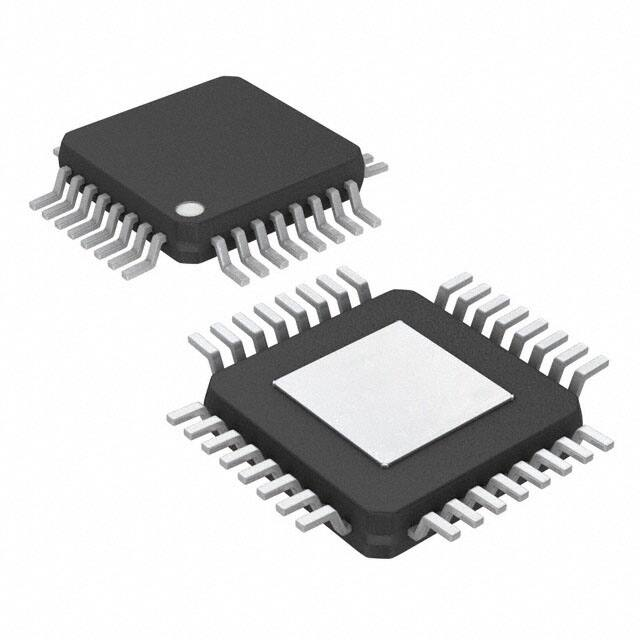
32 TQFP-EP*
MAX3877E/D***
-40°C to +85°C
DICE**
MAX3878EHJ
-40°C to +85°C
32 TQFP-EP*
MAX3878E/D***
-40°C to +85°C
DICE**
* Exposed pad
** Dice are designed to operate over this range, but are tested
and guaranteed at TA = +25°C only. contact factory for availability.
*** Future product—contact factory for availability.
FIL-
PHADJ
LOS
LOL
32
31
30
29
28
27
26
25
GND
1
24 VCC
THADJ
2
23 SDO+
VCC
3
22 SDO-
SDI-
4
SDI+
5
VCC
6
19 SCLKO+
SIS
7
18 SCLKO-
LREF
8
17 VCC
21 VCC
MAX3877
MAX3878
9
10
11
12
13
14
15
16
SLBI+
VCC
VCC
GND
20 VCC
SLBI-
Typical Operating Circuit appears at end of data sheet.
FIL+
TOP VIEW
SONET/SDH Test Equipment
GND
Pin Configuration
CPWD-
DWDM Transmission Systems
SONET/SDH Receivers and Regenerators
Add/Drop Multiplexers
Digital Cross-Connects
♦ Loss-of-Lock Indicator
VCC
Long Haul and Metro Systems with
Optical Amplification
♦ Differential PECL or CML Data and Clock Outputs
♦ Loss-of-Signal Indicator
CPWD+
Applications
♦ Additional 2.488Gbps Input for Diagnostic
Loopback Testing
GND
The MAX3877/MAX3878 are designed for both sectionregenerator and terminal-receiver applications in OC48/STM-16 transmission systems. Their jitter performance
exceeds all of the SONET/SDH specifications. These
devices operate from a single +3.0V to +3.6V supply over
a -40°C to +85°C temperature range. Typical power consumption is only 540mW with a +3.3V supply (MAX3878).
They are available in a 32-pin TQFP-EP package with an
exposed pad, as well as in die form.
♦ Fully Integrated Clock Recovery and Data
Retiming
♦ Optional Holdover Capability (Using External
Reference Clock)
♦ 0.003UIRMS Clock Jitter Generation
♦ Tolerates >2000 Consecutive Identical Digits
GND
These devices provide both loss-of-lock (LOL) and
loss-of-signal (LOS) monitors. Differential CML outputs
are provided for both clock and data signals on the
MAX3877, and differential PECL outputs are provided
for clock and data signals on the MAX3878.
Features
♦ Exceeds ANSI, ITU, and Bellcore SONET/SDH
Specifications
♦ Adjustable Input Threshold (±180mV)
♦ 10mVp-p to 1.2Vp-p Differential Input Range
♦ 540mW Power Dissipation (at +3.3V)
TQFP
________________________________________________________________ Maxim Integrated Products
For pricing, delivery, and ordering information, please contact Maxim/Dallas Direct! at
1-888-629-4642, or visit Maxim’s website at www.maxim-ic.com.
1
MAX3877/MAX3878
General Description
The MAX3877/MAX3878 are compact, low-power clock
recovery and data retiming ICs for 2.488Gbps SONET/
SDH applications. The fully integrated phase-locked
loop (PLL) recovers a synchronous clock signal from
the serial NRZ data input, which is retimed by the
recovered clock. An additional 2.488Gbps serial input
is available for system loopback diagnostic testing, or
this input can be connected to a 155MHz reference
clock to maintain a valid clock output in the absence of
data transitions. The MAX3877/MAX3878 provide vertical threshold and phase-adjust control to optimize system BER in DWDM applications.
�MAX3877/MAX3878
2.5Gbps, +3.3V Clock and Data Retiming ICs
with Vertical Threshold Adjust
ABSOLUTE MAXIMUM RATINGS
Voltage at LOS, SIS, PHADJ, THADJ, CPWD+, CPWD-,
LOL, FIL+, FIL-, LREF.............................-0.5V to (VCC + 0.5V)
Continuous Power Dissipation (TA = +85°C)
32-Pin TQFP-EP (derate 22.2mW/°C above +85°C) ..1444mW
Operating Temperature Range
MAX3877/MAX3878EHJ ..................................-40°C to +85°C
Operating Junction Temperature Range (die) ..-55°C to +150°C
Storage Temperature Range .............................-65°C to +150°C
Processing Temperature (die) .........................................+400°C
Lead Temperature (soldering, 10s) .................................+300°C
Supply Voltage, VCC..............................................-0.5V to +5.5V
Input Voltage Levels
(SDI+, SDI-, SLBI+, SLBI-) ..........(VCC - 0.8V) to (VCC + 0.5V)
Input Current Levels
(SDI+, SDI-, SLBI+, SLBI-)............................-16mA to +10mA
PECL Output Current Levels
(SDO+, SDO-, SCLKO+, SCLKO-) .....................0mA to 56mA
CML Output Current Level
(SDO+, SDO-, SCLKO+, SCLKO-) ...............................±22mA
Current into LOS, LOL .....................................-600µA to +4mA
Stresses beyond those listed under “Absolute Maximum Ratings” may cause permanent damage to the device. These are stress ratings only, and functional
operation of the device at these or any other conditions beyond those indicated in the operational sections of the specifications is not implied. Exposure to
absolute maximum rating conditions for extended periods may affect device reliability.
DC ELECTRICAL CHARACTERISTICS
(VCC = +3.0V to +3.6V, TA = -40°C to +85°C, unless otherwise noted. Typical values are at VCC = +3.3V and TA = +25°C.) (Note 1)
PARAMETER
SYMBOL
CONDITIONS
MIN
TYP
MAX
MAX3877 (Note 2)
175
262
MAX3878 (Note 2)
163
250
UNITS
SUPPLY CURRENT
Supply Current
ICC
mA
INPUT SPECIFICATION (SDI±, SLBI±)
Differential Input Voltage (SDI±)
VID
Differential System Loopback
Input Voltage Range (SLBI±)
Figure 1 (Note 3)
10
1200
mVp-p
VID
50
1200
mVp-p
Single-Ended Input Voltage
(SDI±, SLBI±)
VIS
VCC 0.6
VCC +
0.3
V
Input Termination to VCC
(SDI±, SLBI±)
RIN
Ω
52
MAX3878 PECL OUTPUT SPECIFICATION (SDO±, SCLKO±)
TA = 0°C to +85°C
PECL Output High Voltage
(SDO±, SCLKO±)
TA = -40°C
TA = 0°C to +85°C
PECL Output Low
Voltage (SDO±, SCLKO±)
TA = -40°C
VCC 1.025
VCC 1.085
VCC 1.81
VCC 1.83
VCC 0.88
VCC 0.88
VCC 1.62
VCC 1.556
V
V
MAX3877 CML OUTPUT SPECIFICATION (SDO±, SCLKO±)
CML Differential Output Swing
CML Differential Output
Impedance
CML Output Common-Mode
Voltage
2
RL = 50Ω to VCC
RO
DC-coupling (RL = 50Ω to VCC)
640
800
1000
mVp-p
85
100
115
Ω
VCC 0.2
_______________________________________________________________________________________
V
�2.5Gbps, +3.3V Clock and Data Retiming ICs
with Vertical Threshold Adjust
(VCC = +3.0V to +3.6V, TA = -40°C to +85°C, unless otherwise noted. Typical values are at VCC = +3.3V and TA = +25°C.) (Note 1)
PARAMETER
SYMBOL
CONDITIONS
MIN
TYP
MAX
UNITS
THRESHOLD SETTING SPECIFICATION (SDI±)
Differential Input Voltage Range
VID
Note 4
100
600
mVp-p
Input Threshold Adjustment
Range
VTH
Figure 2
-180
180
mV
VTHADJ
Figure 2
0.2
2.2
V
-5
+5
%
Figure 2
-27
+27
mV
VTH = ±30mV to ±80mV
(Note 5, Figure 2)
-7.0
+7.0
THADJ Voltage Range
Threshold Control Linearity
Threshold Setting Accuracy
mV
Threshold Setting Stability
VTH = ±80mV to ±180mV
(Note 5, Figure 2)
Maximum Input Current (THADJ,
PHADJ)
Control voltage = 0.2V to 2.2V
-11.5
+11.5
-10
+10
µA
TTL INPUT/OUTPUT SPECIFICATION (SIS, LREF, LOL, LOS)
TTL Input High Voltage
(SIS, LREF)
VIH
TTL Input Low Voltage
(SIS, LREF)
VIL
2.0
TTL Input Current
(SIS, LREF)
V
-10
TTL Output High Voltage
(LOL>, LOS)
VOH
IOH = +40µA
TTL Output Low Voltage
(LOL>, LOS)
VOL
IOL = -2mA
0.8
V
+10
µA
2.4
V
0.4
V
AC ELECTRICAL CHARACTERISTICS
(VCC = +3.0V to +3.6V, TA = -40°C to +85°C, unless otherwise noted. Typical values are at VCC = +3.3V and TA = +25°C.)
(Note 6)
PARAMETER
SYMBOL
CONDITIONS
MIN
Serial Output Clock Rate
(Figure 4)
JP
Jitter Transfer Bandwidth
MAX
2.488
Clock-to-Q Delay
Jitter Peaking
TYP
JBW
110
f ≤ 2MHz
1.1
UNITS
Gbps
290
ps
0.1
dB
2.0
MHz
_______________________________________________________________________________________
3
MAX3877/MAX3878
DC ELECTRICAL CHARACTERISTICS (continued)
�MAX3877/MAX3878
2.5Gbps, +3.3V Clock and Data Retiming ICs
with Vertical Threshold Adjust
AC ELECTRICAL CHARACTERISTICS (continued)
(VCC = +3.0V to +3.6V, TA = -40°C to +85°C, unless otherwise noted. Typical values are at VCC = +3.3V and TA = +25°C.)
(Note 6)
PARAMETER
SYMBOL
Jitter Tolerance
Jitter Generation
JGEN
CONDITIONS
MIN
TYP
f = 70kHz
3.18
f = 100kHz (see “Jitter Tolerance” graph in
Typical Operating Characteristics)
2.75
MAX
UNITS
UIp-p
f = 1MHz
0.41
0.67
f = 10MHz
0.36
0.45
0.003
0.006
UIRMS
0.026
0.056
UIp-p
Jitter bandwidth = 12kHz to 20MHz
Clock Output Edge Speed
(20% to 80%)
120
ps
Data Output Edge Speed
(20% to 80%)
120
ps
Tolerated Consecutive Identical
Digits
BER ≤ 10-10
2000
100kHz to 2.5GHz
17
2.5GHz to 4.0GHz
14.5
bits
Input Return Loss (SDI±, SLBI±)
dB
PLL Acquisition Time
14
ms
LOS Assert Time
1.65
µs
LOS Deassert Time
4.0
µs
CPWD = 0.1µF
10
kHz
CFIL = 1µF
6.2
kHz/µs
Low-Frequency Cutoff for
DC-Cancellation Loop
HOLDOVER SPECIFICATION
VCO Frequency Drift Rate in the
Absence of Data
df/dt
PHASE ADJUST SPECIFICATION
Minimum Phase Adjust Range
(Note 7)
-60
+60
ps
Phase Adjust Stability
(Note 8)
-8
+8
ps
Note 1: At TA = -40°C, DC characteristics are guaranteed by design and characterization.
Note 2: Excluding PECL output termination, CML outputs open.
Note 3: Jitter specifications are guaranteed for this data input voltage range, measured by connecting THADJ to VCC. Guaranteed
by design and characterization.
Note 4: Jitter specifications are guaranteed when input threshold is set to ≤ 30% of the differential input swing. Measured with edge
speed ≤ 150ps (Figure 3). Guaranteed by design and characterization.
Note 5: Threshold setting stability is guaranteed by design and characterization.
Note 6: AC characteristics are guaranteed by design and characterization.
Note 7: Phase adjust is disabled when PHADJ is connected to VCC.
Note 8: Phase adjust stability is guaranteed over temperature and power-supply variation.
4
_______________________________________________________________________________________
�2.5Gbps, +3.3V Clock and Data Retiming ICs
with Vertical Threshold Adjust
MAX3877/MAX3878
SDI+
5mV MIN
600mV MAX
SDI-
(SDI+) (SDI-)
VID
10mVp-p MIN
1200mVp-p MAX
Figure 1. Input Amplitude
VTH (mV)
+207
+180
THRESHOLD SETTING ACCURACY
(PART-TO-PART VARIATION OVER PROCESS)
-153
1.1
0.2
THADJ (V)
1.3
2.2
THRESHOLD SETTING STABILITY
(OVER TEMPERATURE OR SUPPLY)
-153
-180
-207
Figure 2. Setting the Input Threshold Level
_______________________________________________________________________________________
5
�(SDI+) - (SDI-) (mV)
+300 (100%)
+180
0 (50%)
VTH RANGE
-180
-300 (0%)
VTH STABILITY
Figure 3. Definition of Input Threshold
tCLK
(SCLKO+) - (SCLKO-)
tCLK-Q
(SDO+)-(SDO-)
Figure 4. Output Clock-to-Q Delay
Typical Operating Characteristics
(VCC = +3.3V, TA = +25°C, unless otherwise noted.)
RECOVERED DATA AND CLOCK
(DIFFERENTIAL OUTPUT)
JITTER TOLERANCE
RECOVERED CLOCK JITTER
MAX3877 toc01
DATA
INPUT JITTER (UIp-p)
TA = +85°C
MAX3877 toc03
PRBS = 223 - 1
PRBS = 223 - 1
PATTERN
VIN = 10mVP-P
10
MAX3877 toc02
MAX3877/MAX3878
2.5Gbps, +3.3V Clock and Data Retiming ICs
with Vertical Threshold Adjust
1
CLOCK
BELLCORE MASK
RMS∆ = 1.33ps
0.1
100ps/div
10ps/div
10
100
1000
JITTER FREQUENCY (kHz)
6
_______________________________________________________________________________________
10,000
�2.5Gbps, +3.3V Clock and Data Retiming ICs
with Vertical Threshold Adjust
JITTER TRANSFER
0.5
0.4
0.3
0.2
10-5
-1.8
-2.1
10-6
10-7
10-8
10-9
PRBS = 223 - 1
100
1000
10,000
10k
100k
1M
10M
JITTER FREQUENCY (Hz)
SUPPLY CURRENT vs. TEMPERATURE
JITTER TOLERANCE vs. PULSE-WIDTH
DISTORTION
240
220
MAX3878
(EXCLUDING PECL OUTPUT CURRENT)
200
180
160
140
120
fJITTER = 5MHz
0.7
0.6
0.5
fJITTER = 10MHz
0.4
INPUT DATA
FILTERED BY
1870MHz 4TH-ORDER
BESSEL FILTER
0.3
0.2
0.1
-50
-25
0
25
50
75
1.5
2.0
2.5
3.0
3.5
PRBS = 223 - 1
INPUT = 300Vp-p
fJITTER = 10MHz
0.7
0.6
0.5
0.4
INPUT DATA
FILTERED BY
1870MHz 4TH-ORDER
BESSEL FILTER
0.3
0.2
0.1
PRBS = 223 - 1
-20
-10
0
10
20
30
20
30
40
50
60
70
AMBIENT TEMPERATURE (°C)
INPUT PULSE-WIDTH DISTORTION (%)
INPUT THRESHOLD (% AMPLITUDE)
JITTER TOLERANCE vs. PHASE ADJUST
JITTER TOLERANCE
vs. INPUT PATTERN-DEPENDENT JITTER
TYPICAL DISTRIBUTION OF 100kHz
JITTER TOLERANCE
0.6
fJITTER = 10MHz
0.4
0.3
0.2
PRBS = 223 - 1
0
-100 -80 -60 -40 -20
fJITTER = 5MHz
0.7
0.6
0.5
fJITTER = 10MHz
0.4
0.3
20 40 60 80 100
PHASE ADJUST (ps)
25
20
15
10
0.2
5
0.1
PRBS = 223 - 1
0
0
0
80
MAX3877 toc12
0.8
PERCENT OF UNITS (%)
fJITTER = 5MHz
SINUSOIDAL JITTER TOLERANCE (Ulp-p)
MAX3877 toc10
0.8
4.0
0
-30
100
1.0
0.8
0
100
0.5
JITTER TOLERANCE vs. THRESHOLD ADJUST
MAX3877 toc08
260
0
DIFFERENTIAL INPUT AMPLITUDE (mVp-p)
0.8
SINUSOIDAL JITTER TOLERANCE (Ulp-p)
MAX3877 toc07
MAX3877
PRBS = 223 - 1
10-10
SINUSOIDAL JITTER TOLERANCE (Ulp-p)
10
280
SUPPLY CURRENT (mA)
-1.5
DIFFERENTIAL INPUT VOLTAGE (mVp-p)
300
SINUSOIDAL JITTER TOLERANCE (Ulp-p)
-1.2
-3.0
1
0.1
-0.9
-2.7
PRBS = 223 - 1
0
0.5
-0.6
10-4
-2.4
0.1
0.7
BELLCORE
MASK
MAX3877 toc09
JITTER FREQUENCY = 5MHz
0.6
0
-0.3
BIT ERROR RATIO
0.7
MAX3877 toc05
MAX3877 toc04
JITTER FREQUENCY = 1MHz
0.8
10-3
MAX3877 toc11
JITTER TOLERANCE (UIp-p)
0.9
BIT ERROR RATIO vs. INPUT AMPLITUDE
0.3
JITTER TRANSFER (dB)
1.0
MAX3877 toc06
JITTER TOLERANCE
vs. INPUT AMPLITUDE
0
10
20
30
40
50
60
PATTERN-DEPENDENT JITTER (ps)
70
80
1.90 1.99 2.08 2.17 2.26 2.35 2.44 2.53 2.62 2.71
100kHz JITTER TOLERANCE (UIp-p)
_______________________________________________________________________________________
7
MAX3877/MAX3878
Typical Operating Characteristics (continued)
(VCC = +3.3V, TA = +25°C, unless otherwise noted.)
�MAX3877/MAX3878
2.5Gbps, +3.3V Clock and Data Retiming ICs
with Vertical Threshold Adjust
Pin Description
8
PIN
NAME
FUNCTION
1, 9, 10,16,
30
GND
Supply Ground
3, 6, 11, 14,
15, 17, 20,
21, 24
VCC
Supply Voltage
2
THADJ
Threshold Control Voltage Input. Used for setting the data decision threshold. Connect to VCC if not
used. See Figure 7.
4
SDI-
Negative Data Input. 2.488Gbps serial data stream.
5
SDI+
Positive Data Input. 2.488Gbps serial data stream.
7
SIS
8
LREF
Signal Input Selection, TTL. High for system loopback input. See Table 1.
Lock to Reference Clock Control Signal, TTL.
12
SLBI-
Negative System Loopback or Reference Clock (in holdover mode) Input
13
SLBI+
Positive System Loopback or Reference Clock (in holdover mode) Input
18
SCLKO-
19
SCLKO+
Positive Clock Output, CML (MAX3877) or PECL (MAX3878)
22
SDO-
Negative Data Output, CML (MAX3877) or PECL (MAX3878)
23
SDO+
Positive Data Output, CML (MAX3877) or PECL (MAX3878)
25
LOL
Loss-of-Lock Indicator, TTL Active-Low
26
LOS
Loss-of-Signal Indicator, TTL Active-High. LOS is asserted high if there are no incoming data
transitions for approximately 1.65µs.
27
PHADJ
28
FIL-
Negative PLL Loop Filter Connection. Connect a 1.0µF capacitor between FIL+ and FIL-.
29
FIL+
Positive PLL Loop Filter Connection. Connect a 1.0µF capacitor between FIL+ and FIL-.
31
CPWD-
Negative Pulse-Width Distortion Cancellation Capacitor. Connect a 0.1µF capacitor between
CPWD+ and CPWD-.
32
CPWD+
Positive Pulse-Width Distortion Cancellation Capacitor. Connect a 0.1µF capacitor between
CPWD+ and CPWD-.
Negative Clock Output, CML (MAX3877) or PECL (MAX3878)
Phase-Adjust Input. Used to optimize sampling point. Connect to VCC if not used. See Figure 6.
_______________________________________________________________________________________
�2.5Gbps, +3.3V Clock and Data Retiming ICs
with Vertical Threshold Adjust
The MAX3877/MAX3878 consist of a fully integrated
phase-locked loop (PLL), input amplifier, data retiming
block, and CML output buffer (MAX3877) or PECL output buffer (MAX3878). The PLL consists of a phase/frequency detector (PFD), a loop filter, and a
voltage-controlled oscillator (VCO). Figure 5 shows the
functional diagram.
This device is designed to deliver the best combination
of jitter performance and power dissipation by using a
fully differential signal architecture and low-noise
design techniques.
SDI Input Amplifier
The SDI input amplifier accepts 2.488Gbps NRZ data
with differential input swing from 10mVp-p up to
1200mVp-p. The bit error rate is better than 1 ✕ 10-10 for
input signals as small as 4mVp-p, though the jitter tolerance performance will be degraded. This amplifier
allows for adjustment of the input threshold level. For
interfacing with PECL signal levels, see Applications
Information, or refer to Applications Note HFAN 1.0,
Interfacing Between CML, PECL, and LVDS.
SLBI Input Amplifier
The SLBI input amplifier accepts either 2.488Gbps
loopback data or a 155MHz reference clock. This
amplifier accepts data with differential input swing from
GND
VCC
50mVp-p up to 1200mVp-p. For interfacing with PECL
signal levels, see Applications Information.
Phase/Frequency Detector
The phase detector incorporated in the MAX3877 and
MAX3878 produces a voltage proportional to the phase
difference between the incoming data and the internal
clock. Because of its feedback nature, the PLL drives
the error voltage to zero, aligning the recovered clock
to the center of the incoming data eye for retiming.
The digital frequency detector (FD) aids frequency
acquisition during startup conditions. The frequency
difference between the received data and the VCO
clock is derived by sampling the in-phase and quadrature VCO output on the rising edges of the data input
signal. The FD drives the VCO until the frequency difference is reduced to zero. Once frequency acquisition
is complete, the FD returns to a neutral state. False
locking is completely eliminated by this digital frequency detector.
While in holdover mode, a Type 4 phase/frequency
detector (PFD) is implemented to track the 155MHz reference clock signal. This PFD compares the incoming
155MHz reference clock with the divided down VCO
clock. The LREF input is used to enable holdover mode
(see Applications Information).
FIL+
CPWD+ CPWD-
FIL-
VCC
THADJ
THRESHOLD
ADJUST
D
AMP
Q
SDO+
SDO-
SDIAMP
SDI+
0
MUX
1
SLBI-
DC-OFFSET/
PWD
CANCELLATION
PHASE &
FREQUENCY
DETECTOR
/16
OR
/1
AMP
SLBI+
SIS
LREF
LOOP
FILTER
LOSS OF
SIGNAL
DETECTOR
LOL
LOS
VCO
Φ
AMP
SCLKO+
SCLKOPHADJ
LOL
LOS
Figure 5. Functional Diagram
_______________________________________________________________________________________
9
MAX3877/MAX3878
Detailed Description
�DC-Offset/Pulse-Width Distortion
Cancellation Loop
PHASE ALIGNMENT vs. PHADJ VOLTAGE
100
PHASE ALIGNMENT (ps)
The input signal is first limited in the forward signal path.
The DC offset of this signal is detected and then amplified
in the feedback path. CPWD sets the cutoff frequency of
the low pass filter. This error signal is then subtracted
from the incoming data. When threshold adjust is
enabled, this loop acts as a pulse-width distortion cancellation loop. Shorting the CPWD± pins together disables
the DC-offset/pulse-width distortion cancellation loop.
50
0
-50
Threshold Adjust
-100
0.2
0.7
1.2
1.7
2.2
PHADJ VOLTAGE
Figure 6. Phase Alignment vs. PHADJ Voltage
Phase Adjust
The internal clock is aligned to the center of the data
eye. For specific applications, this sampling position
can be shifted using the PHADJ input to optimize BER
performance. Refer to Figure 6 for setting the voltage at
PHADJ. When the phase adjust feature is not used,
PHADJ should be tied directly to VCC.
Loop Filter and VCO
The phase detector and frequency detector outputs are
summed into the loop filter. An external capacitor, CF,
is required to set the PLL damping ratio. Refer to
Design Procedure for guidelines on selecting this
capacitor.
The loop filter output controls the on-chip LC VCO running at 2.488GHz. The VCO provides low phase noise
and is trimmed to the correct frequency. Clock jitter
generation is typically 1.2psRMS within a jitter bandwidth of 12kHz to 20MHz.
Loss-of-Lock Monitor
A loss-of-lock monitor is incorporated in the
MAX3877/MAX3878 frequency detector. When the PLL
is frequency locked, the internal LOL signal is high, and
if the PLL is out of frequency lock, the internal LOL signal immediately becomes low.
Loss-of-Signal Detector
A loss of signal detector is provided to detect a loss of
incoming data. If there are no transitions to the SDI
data input for approximately 1.65µs, the LOS signal
becomes high.
This analog input controls the decision threshold of the
input stage. In applications where the noise density is not
balanced between logical zeros and ones (i.e., optical
amplification using EDFA amplifiers), it is possible to
achieve lower bit-error ratios (BER) by adjusting the input
threshold. Threshold adjust may be disabled by connecting THADJ to VCC. The threshold level is set relative to
the center of the differential input voltage swing at the
input. Refer to Figures 3 and 7 for setting the voltage at
THADJ.
Input Select Pins
TTL inputs SIS and LREF are provided to select between
the SDI and SLBI inputs. Table 1 is a logical truth table
describing the operation of SIS and LREF. In this way,
the MAX3877/MAX3878 will automatically lock to the reference clock in the event of a loss-of-signal condition.
In systems where a valid clock output is required under
loss-of-signal conditions, a 155MHz reference clock is
applied to the SLBI inputs for holdover capabilities. This
holdover mode is activated with the LREF input. LREF
may be directly connected to the LOS pin or to an external system loss-of-signal monitor.
THRESHOLD LEVEL vs. VTH VOLTAGE
180
THRESHOLD LEVEL
(mV RELATIVE TO 50%)
MAX3877/MAX3878
2.5Gbps, +3.3V Clock and Data Retiming ICs
with Vertical Threshold Adjust
90
0
-90
-180
0.2
0.7
1.2
1.7
THADJ VOLTAGE
Figure 7. Threshold Level vs. THADJ Voltage
10
______________________________________________________________________________________
2.2
�2.5Gbps, +3.3V Clock and Data Retiming ICs
with Vertical Threshold Adjust
SIS = 0
SIS = 1
LREF = 0
SDI
(Normal Operation)
SLBI
(System Loopback Mode)
LREF = 1
SLBI
(Holdover Mode)
SLBI
(Holdover Mode)
Setting the Loop Filter
The MAX3877/MAX3878 are designed for both regenerator and receiver applications. The fully integrated PLL is a
classic second-order feedback system, with a loop bandwidth (fL) fixed at 1.4MHz. The external capacitor, CF,
can be adjusted to set the loop damping. Figures 8 and 9
show the open-loop and closed-loop transfer functions.
The PLL zero frequency, fZ, is a function of external
capacitor CF, and can be approximated according to:
fZ =
HO(j2πf) (dB)
1
2π(60)CF
OPEN-LOOP GAIN
For an overdamped system (fZ / fL < 0.25), the jitter peaking (MP) of a second-order system can be approximated
by:
CF = 1.0µF
fZ = 2.6kHz
f
MP = 20log 1+ Z
fL
CF = 0.1µF
fZ = 26kHz
f (kHz)
1
100
10
1000
For example, using CF = 0.1µF results in a jitter peaking
of 0.16dB. Reducing CF below 0.01µF may result in PLL
instability. The recommended value of CF = 1.0µF is to
guarantee a maximum jitter peaking of less than 0.1dB.
CF must be a low-TC, high-quality capacitor of type XR7
or better.
Input Termination
Inputs for the MAX3877/MAX3878 are current-mode logic
(CML) compatible. The inputs all provide internal 50Ω termination to reduce the required number of external components. When interfacing to differential PECL levels, it is
important to attenuate the signal while maintaining a 50Ω
termination (see Figure 10). AC-coupling is also necessary to maintain the input common-mode level.
Figure 8. Open-Loop Transfer Function
H(j2πf) (dB)
CF = 0.1µF
0
CLOSED-LOOP GAIN
Output Termination (MAX3877)
-3
The MAX3877 uses current-mode logic (CML) for its highspeed digital outputs. CML outputs are 50Ω back-terminated, reducing the external component count. Refer to
Figure 11 for the output structure. CML outputs may be
terminated by 50Ω to VCC, or by 100Ω differential impedance.
CF = 1.0µF
Output Termination (MAX3878)
f (kHz)
1
10
100
1000
Figure 9. Closed-Loop Transfer Function
The MAX3878 uses positive emitter-coupled logic (PECL)
for its high-speed outputs. PECL outputs are designed to
be terminated by 50Ω to (VCC - 2V). Refer to Applications
Note HFAN 0.1.0, Interfacing Between CML, PECL, and
LVDS, for more information.
______________________________________________________________________________________
11
MAX3877/MAX3878
Design Procedure
Table 1. Selecting Input Path
�MAX3877/MAX3878
2.5Gbps, +3.3V Clock and Data Retiming ICs
with Vertical Threshold Adjust
The BER is better than 1 ✕ 10 -10 for input signals
greater than 4mVp-p. At 5mVp-p, jitter tolerance will be
degraded, but will still be above the SDH/SONET
requirement. The user can make a trade-off between jitter tolerance and input sensitivity according to the specific application. Refer to Typical Operating
Characteristics for Jitter Tolerance and BER vs. Input
Amplitude.
VCC
50Ω
0.1µF
25Ω
50Ω
Applications Information
SDI+
Holdover Mode
PECL
LEVELS
When in holdover mode, the MAX3877/MAX3878 can
lock to an external reference clock to maintain a valid
clock output in the absence of input data. When LREF is
high, the PLL locks to an external 155.52MHz reference
clock, which is applied to the SLBI inputs. To enter
holdover mode automatically when there are no transitions to the SDI inputs, LOS can be directly tied to LREF.
By maintaining frequency lock, the time required to reacquire lock is reduced.
100Ω
0.1µF
SDI-
25Ω
MAX3877
System Loopback
The system loopback input may be used as an auxiliary
input for system loopback testing or as input for an external 155.52MHz reference clock. When used as a loopback test, the user can connect a serializer output in a
transceiver directly to the SLBI inputs for system diagnostics. Using an external reference clock can maintain
PLL frequency lock in the absence of transitions on the
SDI inputs.
Figure 10. Interfacing with PECL Levels
VCC
50Ω
50Ω
SDO+
SDO-
MAX3877
Figure 11. CML Outputs
Jitter Tolerance and Input Sensitivity
Trade-Offs
When the received data amplitude is higher than
10mVp-p, the MAX3877/MAX3878 provide a typical jitter tolerance of 0.64UI at jitter frequencies greater than
10MHz. The SDH/SONET jitter tolerance specification is
0.15UI, leaving a jitter allowance of 0.49UI for receiver
preamplifier and postamplifier design.
12
Consecutive Identical Digits (CID)
The MAX3877/MAX3878 have low frequency drift in the
absence of data transitions. As a result, long runs of consecutive zeros and ones can be tolerated while maintaining a BER better than 1 ✕ 10-10. The CID tolerance is
tested using a 213 - 1PRBS, substituting a long run of
zeros to simulate the worst case. A CID tolerance of
2000 bits is typical.
The VCO frequency after 4096 bits (approximately 1.6µs)
may be estimated by using the VCO drift rate:
6.2kHz
f = 2.488GHz ± 1.65µs ×
µs
= 2.488GHz ± 10.21kHz = 2.488GHz ± 4.1ppm
Exposed Pad (EP) Package
The exposed pad, 32-pin TQFP incorporates features
that provide a very low thermal-resistance path for heat
removal from the IC. The pad is electrical ground on the
MAX3877/MAX3878 and should be soldered to the circuit board for proper thermal and electrical performance.
______________________________________________________________________________________
�2.5Gbps, +3.3V Clock and Data Retiming ICs
with Vertical Threshold Adjust
MAX3877/MAX3878
VCC
VCC
ANALOG INPUTS
VCC
VCC
SDO+
SDO-
SDI-
OUT-
MAX3864
TIA
IN
PHADJ
OUT+
SDI+
VCC
MAX3877/MAX3878 SCKO+
SCKO-
THADJ
SLBI-
LOL
LOS
SLBI+
155MHz
SIS
LREF
TTL
TTL
CML/PECL
CML/PECL
TTL
TTL
Figure 12. Typical Application Circuit (Interfacing with the MAX3864 TIA without using threshold adjust)
Layout Considerations
Performance can be significantly affected by circuit
board layout and design. Use good high-frequency
design techniques, including minimizing ground inductance and using fixed-impedance transmission lines on
the data and clock signals. Power-supply decoupling
should be placed as close to VCC as possible. Take
care to isolate the input from the output signals to
reduce feedthrough.
Chip Information
TRANSISTOR COUNT: 1561
PROCESS: BiPOLAR
SUBSTRATE CONNECTED TO GND
______________________________________________________________________________________
13
�2.5Gbps, +3.3V Clock and Data Retiming ICs
with Vertical Threshold Adjust
MAX3877/MAX3878
Typical Application Circuit
VCC
1.0µF
1.0µF
VCC
GND VCC FIL+
FIL- CPWD+ CPWDSDO+
SDO-
CML/PECL
SCLKO+
SCLKO-
CML/PECL
SDIIN
TIA
AGC
MAX3877/MAX3878
SDI+
THADJ
SLBI-
LOL
LOS
SLBI+
ANALOG
INPUT
155MHz HOLDOVER
REFERENCE CLOCK OR
2.5Gbps SYSTEM
LOOPBACK DATA
PHADJ
SIS
LREF
ANALOG
INPUT
TTL
TTL
TTL
TTL
Chip Topography
LOL
LOS
PHADJ
N.C.
FIL-
N.C.
FIL+
GND
CPWD-
CPWD+
0.091in
2.311mm
GND
N.C.
GND
VCC
GND
SDO+
GND
SDOTHADJ
VCC
VCC
GND
VCC
SDI+
SCLKO+
SDI-
GND
N.C.
VCC
N.C.
GND
VCC
LRE
SLBI+
VCC
SLBI-
SIS
VCC
SCLKO-
GND
VCC
GND
14
0.09in
2.286mm
______________________________________________________________________________________
�2.5Gbps, +3.3V Clock and Data Retiming ICs
with Vertical Threshold Adjust
32L,TQFP.EPS
______________________________________________________________________________________
15
MAX3877/MAX3878
Package Information
�2.5Gbps, +3.3V Clock and Data Retiming ICs
with Vertical Threshold Adjust
MAX3877/MAX3878
Package Information (continued)
Maxim cannot assume responsibility for use of any circuitry other than circuitry entirely embodied in a Maxim product. No circuit patent licenses are
implied. Maxim reserves the right to change the circuitry and specifications without notice at any time.
16 ____________________Maxim Integrated Products, 120 San Gabriel Drive, Sunnyvale, CA 94086 408-737-7600
© 2001 Maxim Integrated Products
Printed USA
is a registered trademark of Maxim Integrated Products.
�


 工商网监
湘ICP备2023018690号
工商网监
湘ICP备2023018690号
