EVALUATION KIT AVAILABLE
MAX40008/MAX40009
General Description
The MAX40008/MAX40009 are single micro-power
comparators featuring low-voltage operation and
rail-to-rail inputs. Their operating supply voltage range
from 1.7V to 5.5V, which makes them ideal for systems
running from nominal 1.8V to 5V supplies.
While only consuming 12μA of supply current, the
MAX40008/MAX40009 achieve a 220ns propagation delay.
These devices feature 0.5mV (typ) input offset voltage and
internal hysteresis, ensuring clean output switching, even
with slow-moving input signals.
The output stage’s unique design limits supply-current
surges while switching, virtually eliminating the supply
glitches typical of many other comparators. The MAX40009
has a push-pull output stage, while the MAX40008 has an
open-drain output stage that can be pulled beyond VDD to
6V (max) above GND input. The open-drain version is ideal
for level translators and bipolar to single-ended converters.
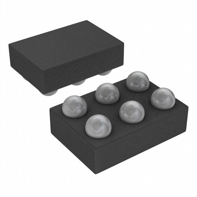
The MAX40008/MAX40009 are available in tiny 0.73mm
x 1.1mm 6-bump wafer-level packages (WLPs),
significantly reducing the required board area. An alternative
6-pin SOT23 package is also available. These devices are
fully specified over the -40°C to +125°C automotive
temperature range.
Applications
●● Mobile Communications
●● Portable/Battery-Powered Systems
●● Window Comparators
●● Level Translators
●● Threshold Detectors/ Discriminators
●● IR Receivers
19-8737; Rev 1; 5/17
220ns, 12μA, 6-Bump WLP
Comparators with Shutdown
Benefits and Features
●● 220ns Propagation Delay
●● Tiny 0.73mm x 1.1mm with 0.35mm Pitch 6-Bump
WLP and SOT23 Packages Save Board Space
●● Rail-to-Rail Inputs
●● Low Operating Current ≤ 17μA (max) Over
Temperature
●● No Phase Reversal for Overdriven Inputs
●● Integrated RF Immunity Filters
●● Supply Voltage Range (1.7V to 5.5V) Allows
Operation from 1.8V, 2.5V, 3V, and 5V Supplies
●● Push-Pull (MAX40009) or Open-Drain (MAX40008)
Outputs
●● -40°C to +125°C Temperature Range
●● Low-Power Shutdown Input Reduces Quiescent
Current to 150nA
Ordering Information appears at end of data sheet.
�MAX40008/MAX40009
220ns, 12μA, 6-Bump WLP
Comparators with Shutdown
Simplified Block Diagram
VDD
SHDN
VDD
GND
GND
IN-
INOUT
IN+
MAX40009
GND
www.maximintegrated.com
SHDN
OUT
IN+
MAX40008
GND
Maxim Integrated │ 2
�MAX40008/MAX40009
220ns, 12μA, 6-Bump WLP
Comparators with Shutdown
Absolute Maximum Ratings
VDD to GND.............................................................-0.3V to +6V
IN+, IN-, SHDN to GND...........................................-0.3V to +6V
IN+ to IN-................................................................................±6V
OUT(MAX40008) to GND........................................-0.3V to +6V
OUT(MAX40009) to GND............................-0.3V to VDD + 0.3V
OUT Short-Circuit to VDD or GND Duration........................... 10s
Continuous Current Into Any Input Pin................................20mA
Continuous Current Into/Out of Any Output Pin..................50mA
Maximum Power Dissipation........................................................
WLP-6, Derate 10.2mW/°C Above +70°C....................816mW
SOT23-6, Derate 4.3mW/°C Above +70°C...............347.8mW
Operating Temperature Range.......................... -40°C to +125°C
Junction Temperature.......................................................+150°C
Storage Temperature Range............................. -65°C to +150°C
Lead Temperature (Soldering, 10s).................................. +300°C
Stresses beyond those listed under “Absolute Maximum Ratings” may cause permanent damage to the device. These are stress ratings only, and functional operation of the device at these
or any other conditions beyond those indicated in the operational sections of the specifications is not implied. Exposure to absolute maximum rating conditions for extended periods may affect
device reliability.
Package Information
6-WLP
PACKAGE CODE
N60D1+1
Outline Number
21-100086
Land Pattern Number
Refer to Application Note 1891
THERMAL RESISTANCE, FOUR-LAYER BOARD:
Junction to Ambient (θJA)
98°C/W
Junction to Case (θJC)
6-SOT23
PACKAGE CODE
U6+1
Outline Number
21-0058
Land Pattern Number
90-0175
THERMAL RESISTANCE, FOUR-LAYER BOARD:
Junction to Ambient (θJA)
230°C/W
Junction to Case (θJC)
76°C/W
For the latest package outline information and land patterns (footprints), go to www.maximintegrated.com/packages. Note that a “+”,
“#”, or “-” in the package code indicates RoHS status only. Package drawings may show a different suffix character, but the drawing
pertains to the package regardless of RoHS status.
Package thermal resistances were obtained using the method described in JEDEC specification JESD51-7, using a four-layer board.
For detailed information on package thermal considerations, refer to www.maximintegrated.com/thermal-tutorial.
www.maximintegrated.com
Maxim Integrated │ 3
�MAX40008/MAX40009
220ns, 12μA, 6-Bump WLP
Comparators with Shutdown
Electrical Characteristics
(VDD = VSHDN = 3.3V, VCM = 0V, RPULLUP = 39kΩ from OUT to VDD = 3.3V (for MAX40008 only), RLOAD = open circuit, CLOAD = 15pF,
TA = TMIN to TMAX. Typical values are at TA = +25°C, unless otherwise noted (Note 1))
PARAMETER
SYMBOL
CONDITIONS
MIN
TYP
MAX
UNITS
5.5
V
17
μA
POWER SUPPLY SPECIFICATIONS
Supply Voltage Range
Supply Current
Supply Current in
Shutdown Mode
VDD
IDD
IDD
Shutdown Input Current
Guaranteed by PSRR specification
1.7
No output or load current, output is high,
1.7V ≤ VDD ≤ 5.5V, TA = -40°C to +125°C
No output or load current, output is high,
TA = +25°C
12
µA
VSHDN = GND, TA = -40°C to +125°C
1
VSHDN = VDD
1
VSHDN = GND
Shutdown Input
Voltage Low
Shutdown logic-level low
Shutdown Input Voltage
High
Shutdown logic-level high
1
0.55
1.3
Power-Up Time
μA
μA
V
V
50
µs
COMPARATOR
Input Common Mode
Range
VCM
Input Offset Voltage
(Note 2)
Guaranteed by CMRR specification,
TA = +25°C
-0.2
Guaranteed by CMRR specification
TA = -40°C to 125°C
0
VCM = 1.65V = VDD/2, TA = -40°C to
+125°C
Common Mode Rejection Ratio
CMRR
Input Hysteresis
(Note 3)
VHYS
VDD +
0.2
VDD
±0.5
52
3
mV
Input Capacitance
Either input, over entire VCM range
1
Power Supply
Rejection Ratio
DC, over the entire common mode input
range (VCM), measured at VCM = 0V and
VCM = VDD
Output Voltage
Swing Low
www.maximintegrated.com
VOL
mV
dB
20
IB
±5
70
Over the common mode input range
(VCM), TA = -40°C to +125°C
Input Bias Current
V
140
nA
pF
60
dB
Sinking 8mA output current, V(OUT-GND)
at VDD = 3.3V
0.4
Sinking 1.6mA output current, V(OUT-GND)
at VDD = 1.7V
0.4
V
Maxim Integrated │ 4
�MAX40008/MAX40009
220ns, 12μA, 6-Bump WLP
Comparators with Shutdown
Electrical Characteristics (continued)
(VDD = VSHDN = 3.3V, VCM = 0V, RPULLUP = 39kΩ from OUT to VDD = 3.3V (for MAX40008 only), RLOAD = open circuit, CLOAD = 15pF,
TA = TMIN to TMAX. Typical values are at TA = +25°C, unless otherwise noted (Note 1))
PARAMETER
Output Voltage Swing
High
Propagation Delay
(Note 4)
SYMBOL
VOH
tPD
CONDITIONS
MIN
TYP
MAX
Sourcing 1.6mA output current, V(DD-OUT)
at VDD = 1.7V
0.6
Sourcing 8mA output current, V(DD-OUT) at
VDD = 3.3V
0.6
UNITS
V
100mV overdrive, output L->H, MAX40009
220
100mV overdrive, output L->H, MAX40008;
RPULLUP = 39kΩ
650
100mV overdrive, output H->L, MAX40008/
MAX40009
235
20mV overdrive, output L->H, MAX40009
245
20mV overdrive, output L->H, MAX40008;
RPULLUP = 39kΩ
850
20mV overdrive, output H->L, MAX40008/
MAX40009
340
ns
Rise Time
tR
MAX40009, 25% to 75% output swing
1.7
ns
Fall Time
tF
MAX40008/MAX40009: 75% to 25% output
swing
1.4
ns
Note 1: All specifications are 100% production tested at TA = +25°C. Specification limits over temperature (TA = TMIN to TMAX) are
guaranteed by design, not production tested.
Note 2: Input offset voltage; VOS is defined as the center of the hysteresis band or average of the threshold trip points.
Note 3: The hysteresis-related trip points are defined as the edges of the hysteresis band, measured with respect to the center of
the band (i.e., VOS) (Figure 1).
Note 4: Propagation Delay measurement is from 20% of the input to 80% of the output.
www.maximintegrated.com
Maxim Integrated │ 5
�MAX40008/MAX40009
220ns, 12μA, 6-Bump WLP
Comparators with Shutdown
Typical Operating Characteristics
(VDD = VSHDN = 3.3V, VCM = 0V, RPULLUP = 39kΩ from OUT to VDD = 3.3V (for MAX40008 only), RLOAD = open circuit, CLOAD = 15pF,
TA = TMIN to TMAX. Typical values are at TA = +25ºC, unless otherwise noted (Note 1))
toc01
13.5
SUPPLY CURRENT
vs. OUTPUT TRANSITIONFREQUENCY
SUPPLY CURRENT
vs. OUTPUT TRANSITIONFREQUENCY
SUPPLY CURRENT vs. SUPPLY VOLTAGE
toc02a
30
toc02b
50
VDD = 3.3V
VDD = 1.7V
25
TA = +85°C
11.5
TA = -40°C
10.5
40
SUPPLY CURRENT (µA)
SUPPLY CURRENT (µA)
SUPPLY CURRENT (µA)
TA = +25°C
12.5
20
TA = +25°C
15
10
TA = -40°C
5
30
TA = +25°C
20
10
VOUT = HIGH
2
2.5
3
3.5
4
4.5
5
5.5
0.1
6
10
100
SUPPLY VOLTAGE (V)
OUTPUT TRANSISTION FREQUENCY (kHz)
SUPPLY CURRENT
vs. OUTPUT TRANSITIONFREQUENCY
SHUTDOWNSUPPLY CURRENT
vs. TEMPERATURE
toc02c
VDD = 5.5V
TA = +125°C
400
300
200
100
TA = -40°C
TA = +25°C
0
1
10
100
0.4
VDD = 3.3V
0.2
0.15
VDD = 1.7V
0.1
-40 -25 -10 5
toc04b
0
2
4
6
SINK CURRENT (mA)
8
toc04c
500
OUTPUT VOLTAGE LOW (V) (VOUT )
OUTPUT VOLTAGE LOW (V) (VOUT )
100
OUTPUT VOLTAGELOW
vs. SINK CURRENT
VDD = 5.5V
VDD = 3.3V
TA = +125°C
500
400
TA = +25°C
300
200
TA = -40°C
100
TA = +125°C
200
0
20 35 50 65 80 95 110 125
TEMPERATURE (°C)
OUTPUT VOLTAGELOW
vs. SINK CURRENT
600
TA = +25°C
300
TA = -40°C
0
1000
100
VDD = 1.7V
0.05
OUTPUT TRANSISTION FREQUENCY (kHz)
700
10
toc 04a
400
0.3
0.25
1
OUTPUT VOLTAGELOW
vs. SINK CURRENT
VDD = 5.5V
0.35
TA = -40°C
0.1
OUTPUT TRANSISTION FREQUENCY (kHz)
toc03
0.45
SHUTDOWN SUPPLY CURRENT (µA)
500
0.1
1
OUTPUT VOLTAGE LOW (V) (VOUT )
1.5
SUPPLY CURRENT (µA)
0
0
9.5
TA = +125°C
400
TA = +25°C
300
200
100
TA = -40°C
0
0
0
5
10
15
20
SINK CURRENT (mA)
www.maximintegrated.com
25
30
0
5
10
15
20
25
30
35
SINK CURRENT (mA)
Maxim Integrated │ 6
�MAX40008/MAX40009
220ns, 12μA, 6-Bump WLP
Comparators with Shutdown
Typical Operating Characteristics (continued)
(VDD = VSHDN = 3.3V, VCM = 0V, RPULLUP = 39kΩ from OUT to VDD = 3.3V (for MAX40008 only), RLOAD = open circuit, CLOAD = 15pF,
TA = TMIN to TMAX. Typical values are at TA = +25ºC, unless otherwise noted (Note 1))
OUTPUT VOLTAGEHIGH
vs. SOURCE CURRENT
OUTPUT VOLTAGEHIGH
vs. SOURCE CURRENT
1.4
1.2
TA = +125°C
1
0.8
0.6
TA = +25°C
0.4
0.2
TA = -40°C
0
0
1
2
3
toc05b
3.4
3.2
3
2.8
2.6
2.4
2.2
2
1.8
1.6
1.4
1.2
1
0.8
0.6
0.4
0.2
0
4
TA = +25°C
TA = -40°C
toc06
5
10
15
20
SOURCE CURRENT (mA)
25
40
VDD = 3.3V
30
20
VDD = 1.7V
10
0
50
100
TEMPERATURE (°C)
0.25
TA = -40°C
30
20
VDD = 1.7V
-0.5
VDD = 1.7V
-1
VDD = 5.5V
VDD = 3.3V
-1.5
0
50
100
TEMPERATURE (°C)
150
-40
toc10a
300
110
toc10b
400
VOD = 100mV
VDD = 5.5V
300
VDD = 3.3V
tPD+ (ns)
200
tP D- (ns)
HYSTERESIS (mV)
10
60
TEMPERATURE (°C)
PROPAGATION DELAY(tPD+)
vs. TEMPERATURE
VDD = 3.3V
2
30
toc08
3.5
VDD = 1.7V
25
10
VDD = 1.7V
2.5
20
0
PROPAGATION DELAY(tPD-)
vs. TEMPERATURE
VDD = 3.3V
15
INPUT OFFSET VOLTAGE
vs. TEMPERATURE
VDD = 3.3V
40
-50
3
10
SOURCE CURRENT (mA)
50
150
toc09
5
VDD = 5.5V
60
HYSTERESIS vs. TEMPERATURE
4
0.5
0
0
0
TA = +25°C
30
toc07
70
SHORT CIRCUIT SOURCE CURRENT (mA)
50
-50
0.75
SHORT CIRCUIT SOURCE CURRENT
vs. TEMPERATURE
VDD = 5.5V
TA = +125°C
0
0
SHORT CIRCUIT SINK CURRENT
vs. TEMPERATURE
SHORT CIRCUIT SINK CURRENT (mA)
VDD = 5.5V
TA = +125°C
SOURCE CURRENT (mA)
60
toc05c
1
VDD = 3.3V
INPUT OFFSET VOLTAGE (mV)
1.6
OUTPUT VOLTAGE HIGH (V) (VDD - VOUT )
OUTPUT VOLTAGE HIGH (V) (VDD - VOUT )
VDD = 1.7V
OUTPUT VOLTAGE HIGH (V) (VDD - VOUT )
toc05a
1.8
OUTPUT VOLTAGEHIGH
vs. SOURCE CURRENT
VDD = 5.5V
200
VDD = 1.7V
100
100
1.5
VDD = 5.5V
VOD = 100mV
1
-40
10
60
TEMPERATURE (°C)
www.maximintegrated.com
110
0
0
-40
10
60
TEMPERATURE (°C)
110
-40
10
60
TEMPERATURE (°C)
110
Maxim Integrated │ 7
�MAX40008/MAX40009
220ns, 12μA, 6-Bump WLP
Comparators with Shutdown
Typical Operating Characteristics (continued)
(VDD = VSHDN = 3.3V, VCM = 0V, RPULLUP = 39kΩ from OUT to VDD = 3.3V (for MAX40008 only), RLOAD = open circuit, CLOAD = 15pF,
TA = TMIN to TMAX. Typical values are at TA = +25ºC, unless otherwise noted (Note 1))
PROPAGATION DELAY(tPD-)
vs. CAPACITIVE LOAD
PROPAGATION DELAY(tPD+)
vs. CAPACITIVE LOAD
toc11a
800
900
VDD = 3.3V
700
800
700
600
500
VOD = 20mV
tPD+ (ns)
tPD- (ns)
600
400
300
500
VOD = 20mV
400
300
200
200
VOD = 100mV
100
VOD = 100mV
100
0
0
0.01
0.1
1
CAPACITIVE LOAD (nF)
0.01
10
0.1
1
10
CAPACITIVE LOAD (nF)
PROPAGATION DELAY(tPD+)
vs. INPUT OVERDRIVE
PROPAGATION DELAY(tPD-)
vs. INPUT OVERDRIVE
toc12a
900
toc12b
500
VDD = 5.5V
800
400
700
500
VDD = 1.7V
400
tP D+ (ns)
600
tPD- (ns)
toc11b
VDD = 3.3V
VDD = 3.3V
300
VDD = 3.3V
200
300
200
100
VDD = 1.7V
VDD = 5.5V
100
0
0
40
80
120
160
0
200
0
OVERDRIVE VOLTAGE (mV)
PROPAGATION DELAY_tPD+
40
80
120
160
OVERDRIVE VOLTAGE (mV)
PROPAGATION DELAY_tPD-
toc13a
IN+
VOUT
(2V/div)
www.maximintegrated.com
toc13b
IN+
(100mV/div)
(100mV/div)
100ns/div
200
VOUT
(2V/div)
200ns/div
Maxim Integrated │ 8
�MAX40008/MAX40009
220ns, 12μA, 6-Bump WLP
Comparators with Shutdown
Typical Operating Characteristics (continued)
(VDD = VSHDN = 3.3V, VCM = 0V, RPULLUP = 39kΩ from OUT to VDD = 3.3V (for MAX40008 only), RLOAD = open circuit, CLOAD = 15pF,
TA = TMIN to TMAX. Typical values are at TA = +25ºC, unless otherwise noted (Note 1))
1MHz FREQUENCY RESPONSE
(COUT = 10pF)
SWITCHING CURRENT, OUTPUT RISING
toc 15
toc14
400mV
400mV
VIN
VIN
(200mV/div)
0
(200mV/div)
0
3.3V
VOUT
3.3V
(2V/div)
VOUT
(2V/div)
0
0
ICC
(1mA/div)
200ns/div
40ns/div
SHUTDOWNENABLE TRANSIENT
SWITCHING CURRENT, OUTPUT FALLING
toc 17
toc16
400mV
VIN
3.3V
VSHDN
(200mV/div)
0
(2V/div)
(200mV/div)
0
3.3V
VOUT
(2V/div)
3.3V
VOUT
0
ICC
(1mA/div)
(2V/div)
0
1ms/div
200μ s/div
40ns/div
SHUTDOWNDISABLE TRANSIENT
toc 18
3.3V
VSHDN
(2V/div)
(200mV/div)
0
3.3V
VOUT
(2V/div)
0
1ms/div
200μ s/div
www.maximintegrated.com
Maxim Integrated │ 9
�MAX40008/MAX40009
220ns, 12μA, 6-Bump WLP
Comparators with Shutdown
Pin Configuration
MAX40008/MAX40009 (6 WLP)
MAX40008/MAX40009 (6 SOT23)
TOP VIEW
TOP VIEW
2
+
3
IN-
1
GND
2
/SHDN\
3
+
1
A
B
IN+
VDD
OUT
IN-
/SHDN\
GND
MAX40008ANT+
MAX40009ANT+
MAX40008AUT+
MAX40009AUT+
WLP
6
IN+
5
VDD
4
OUT
SOT-23
Pin Description
PIN
MAX40008/
MAX40009
(6 WLP)
MAX40008/
MAX40009
(6-SOT23)
NAME
A1
6
IN+
Non-Inverting Input of the Comparator.
A2
5
VDD
Positive Supply Voltage Input. Bypass with a 0.1μF capacitor to GND as close to
the device's supply input as possible.
B1
1
IN-
A3
4
OUT
B2
3
SHDN
B3
2
GND
www.maximintegrated.com
FUNCTION
Inverting Input of the Comparator.
Open-Drain Output (MAX40008) or Push-Pull Output (MAX40009). For open-drain
version, connect a 39kΩ pullup resistor from OUT to any pullup voltage up to 5.5V.
Shutdown Input. Active-low input. The device enters into shutdown when SHDN
input is low. The device is active when SHDN input is high.
Ground/Signal and Power Return.
Maxim Integrated │ 10
�MAX40008/MAX40009
Detailed Description
The MAX40008/MAX40009 are single, low-power, lowvoltage comparators with shutdown. They have an operating
supply voltage range between 1.7V and 5.5V, while
consuming only 12μA of supply current. Their commonmode input voltage range extends 200mV beyond each
rail. Internal hysteresis ensures clean output switching,
even with slow-moving input signals. Large internal output
drivers allow rail-to-rail output swing with up to 8mA loads.
The output stage employs a unique design that minimizes
supply current surges while switching, virtually eliminating
the supply glitches typical of many other comparators.
The MAX40008 has an open-drain output that can be
pulled beyond VDD to an absolute maximum of 6V above
GND input.
Applications Information
Internal Hysteresis
Many comparators oscillate in the linear region of operation
because of noise or undesired parasitic feedback. This
tends to occur when the voltage on one input is equal
to, or very close to, the voltage on the other input. The
MAX40008/MAX40009 have internal 3mV hysteresis to
counter parasitic effects and noise.
220ns, 12μA, 6-Bump WLP
Comparators with Shutdown
The hysteresis in a comparator creates two trip points: one for
the upper threshold (VTRIP+) and one for the lower threshold
(VTRIP-) for voltage transitions on the input signal (Figure 1).
The difference between the trip points is the hysteresis
band (VHYST). When the comparator’s input voltages are
equal, the hysteresis effectively causes one comparator
input to move quickly past the other, thus taking the input
out of the region where oscillation occurs. Figure 1 illustrates
the case in which IN- has a fixed voltage applied, and IN+
is varied. If the inputs were reversed, the figure would be
the same, except with an inverted output.
Component Selection
When employing an additional external hysteresis, the
highest impedance circuits should be used wherever
possible. The offset error due to input bias current is
proportional to the total impedance seen at the input. For
example, selecting components for Figure 2, with a target
of 50mV hysteresis, a 5V supply, and choosing an RF of
10MΩ gives RG as 100kΩ. The total impedance seen at
IN+ is, therefore, 10MΩ || 100kΩ, or 99kΩ. The input bias
current of MAX40008/MAX40009 is 20nA. Therefore, the
error due to source impedance is less than 2000μV.
Figure 1. Hysteresis Band
www.maximintegrated.com
Maxim Integrated │ 11
�MAX40008/MAX40009
220ns, 12μA, 6-Bump WLP
Comparators with Shutdown
Board Layout and Bypassing
Use 100nF bypass capacitors close to the device’s supply
inputs when supply impedance is high, supply leads are
long, or excessive noise is expected on the supply lines.
Minimize signal trace lengths to reduce stray capacitance.
A ground plane and surface-mount compo
nents are
recommended.
Data Recovery
Figure 3 shows a time averaging of the input signal for data
recovery. Digital data is often embedded into a bandwidth
and amplitude-limited analog path. Recovering the data
can be difficult. A simple circuit in Figure 3 compares the
input signal to a time-averaged version of itself. This selfbiases the threshold voltage to the average input voltage
for optimal noise margin. Even severe phase distortion
RG
is eliminated from the digital output signal. Be sure to
choose R1 and C1 so that:
fCAR >> 1/(2πR1C1)
fCAR is the fundamental frequency of the input digital data
stream.
Logic Level Translator
The Typical Application Circuit shows an application that
converts 3.3V logic to 1.8V logic levels. The MAX40008
is powered by the +3.3V supply voltage to VDD, and the
pullup resistor for the MAX40008’s open-drain output is
connected to the +1.8V supply voltage. This configuration
allows the full 3.3V logic swing without creating overvoltage
on the 1.8V logic inputs. For 1.8V to 3.3V logic-level
translations, simply connect the +1.8V supply voltage to
VDD and the +3.3V supply voltage to the pullup resistor.
RF
VIN+
VDD
VTHRESHOLD
MAX40009
Figure 2. Additional External Hysteresis on MAX40009
www.maximintegrated.com
Figure 3. Time Averaging of the Input Signal for Data Recovery
Maxim Integrated │ 12
�MAX40008/MAX40009
220ns, 12μA, 6-Bump WLP
Comparators with Shutdown
Typical Application Circuit
Logic Level Translator
Ordering Information
TEMP RANGE
PIN-PACKAGE
TOP MARK
MAX40008ANT+T
PART NUMBER
-40°C to +125°C
6 WLP
+3
MAX40009ANT+T
-40°C to +125°C
6 WLP
+4
MAX40008AUT+T*
-40°C to +125°C
6 SOT23
+ACUW
MAX40009AUT+T*
-40°C to +125°C
6 SOT23
+ACUX
+ Denotes a lead(Pb)-free/RoHS-compliant package.
T = Tape and reel.
Future Product—Contact factory for availability.
www.maximintegrated.com
Maxim Integrated │ 13
�MAX40008/MAX40009
220ns, 12μA, 6-Bump WLP
Comparators with Shutdown
Revision History
REVISION
NUMBER
REVISION
DATE
0
1
12/16
5/17
PAGES
CHANGED
DESCRIPTION
Initial release
Removed future product asterisk from MAX40008ANT+T part number
—
13
For pricing, delivery, and ordering information, please contact Maxim Direct at 1-888-629-4642, or visit Maxim Integrated’s website at www.maximintegrated.com.
Maxim Integrated cannot assume responsibility for use of any circuitry other than circuitry entirely embodied in a Maxim Integrated product. No circuit patent licenses
are implied. Maxim Integrated reserves the right to change the circuitry and specifications without notice at any time. The parametric values (min and max limits)
shown in the Electrical Characteristics table are guaranteed. Other parametric values quoted in this data sheet are provided for guidance.
Maxim Integrated and the Maxim Integrated logo are trademarks of Maxim Integrated Products, Inc.
© 2017 Maxim Integrated Products, Inc. │ 14
�