EVALUATION KIT AVAILABLE
Click here for production status of specific part numbers.
MAX40016
General Description
The MAX40016 is a very wide range current sense amplifier
(CSA) with internal sense element that senses from less
than 300µA to greater than 3A current range. The 4-decade
sensed current functions with 1% (typical) gain error and
offers three, multiplexed programmable output ranges in
order to interface with 12-bit ADCs. Having an integrated
sense element has the extra advantage that the entire
current measuring path can be factory-trimmed, saving the
user from having to calibrate independent sense resistors
and CSAs. The MAX40016 (WLP package) drops a typical
of 60mV at 3A from the voltage input to load output.
The MAX40016's integrated current-sensing element
saves the space and cost of an external high-power,
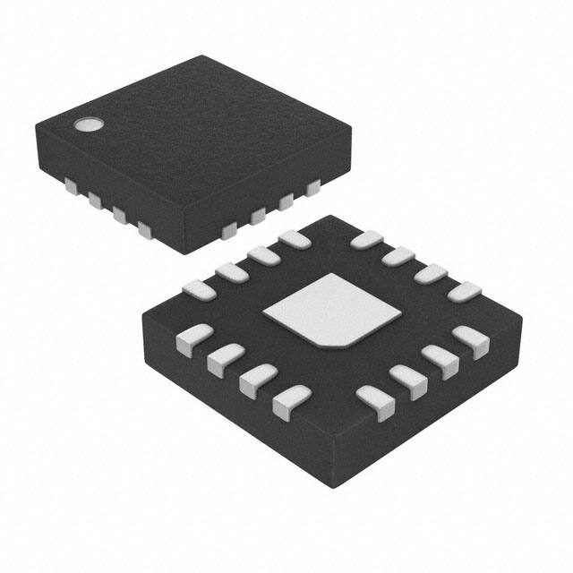
precision current sense resistor. The MAX40016 is offered
in an ultra-tiny, 1.98mm x 1.31mm, 15-bump waferlevel package (WLP), further reducing board space. The
MAX40016 is also available in a 4mm x 4mm 16-pin
TQFN package.
The MAX40016 operates with a supply voltage from 2.5V
to 5.5V. The device features a low-power mode in which
the current-sensing element remains on, but the outputs
are turned off to reduce the total supply current below
10µA (max).
The MAX40016 also includes a committed on-board
amplifier with an internal gain of 1.5V/V. The MAX40016
operates over the -40°C to +125°C temperature range.
Applications
●● Mobile Devices
●● RF Power Monitoring
●● Portable Instruments
19-100232; Rev 2; 11/18
4-Decade Current Sense Amplifier
with Integrated Current Sense Element
Benefits and Features
●● Integrated Current Sense Element Saves The Space
and Cost of Expensive Precision Sense Resistors
●● 4-Decade Measurement Range
• Maintains Accuracy from < 300µA to > 3A
●● Withstands Overloads to 4A
●● Low Voltage Drop Across Sense Element
• 60mV (Active Mode, 3A Load, WLP Package)
• 35mV (Low Power Mode, 3A Load, WLP Package)
●● Three Multiplexed Scaling Resistor Outputs Allow
Full Dynamic Range while Interfaced to 12-bit ADCs
●● +2.5V to +5.5V Input Supply Voltage Range
●● Low Power Mode Reduces Supply Current to 10µA
Max
●● Space-Saving
• Tiny 1.98mm x 1.3mm, 15-Bump WLP
• 4mm x 4mm 16-Pin TQFN
●● -40°C to +125°C Operating Temperature Range
Ordering Information appears at end of data sheet.
�MAX40016
4-Decade Current Sense Amplifier
with Integrated Current Sense Element
Simplified Block Diagram
INPUT 2.5V to 5.5V
MEA SURED
AT UP TO 3A
CURRENT
CIN
MAX40016
LD
VDD
ISH
RISH
CLD
160Ω
ISM
CURRENT
MI RROR
CONTROL
RISM
5.36kΩ
ISL
RISL
160kΩ
SEL0
FROM
CONTROLLER
SEL1
RANGE
SELE CTION
VOUT
GNDS
ROUT
COUT
GND
www.maximintegrated.com
Maxim Integrated │ 2
�MAX40016
4-Decade Current Sense Amplifier
with Integrated Current Sense Element
Absolute Maximum Ratings
VDD to GND.............................................................-0.3V to +6V
GND to GNDS.......................................................-0.3V to +0.3V
SEL0, SEL1, ISL, ISM, ISH, VOUT to GND...-0.3V to VDD+0.3V
VDD to LD................................................................-0.3V to 0.3V
LD to GND.......................................... VDD - 0.3V to VDD + 0.3V
Maximum Current
( All pins except VDD, LD, continuous)............................20mA
Current from VDD to LD (Continuous)......................................4A
Continuous Power Dissipation (TA = +70°C)
15-Bump WLP (derate 14.39mW/°C above +70°C)...... 1151.2mW
16-Pin TQFN (derate 25mW/°C above +70°C)..............2000mW
Operating Temperature Range.......................... -40°C to +125°C
Junction Temperature.......................................................+150°C
Storage Temperature Range............................. -65°C to +150°C
Soldering Temperature (reflow)........................................+260°C
Stresses beyond those listed under “Absolute Maximum Ratings” may cause permanent damage to the device. These are stress ratings only, and functional operation of the device at these
or any other conditions beyond those indicated in the operational sections of the specifications is not implied. Exposure to absolute maximum rating conditions for extended periods may affect
device reliability.
Package Information
15 WLP
PACKAGE CODE
N151B1+1
Outline Number
21-100213
Land Pattern Number
Refer to Application Note 1891
THERMAL RESISTANCE, MULTI-LAYER BOARD:
Junction to Ambient (θJA)
69.5°C/W
Junction to Case (θJC)
N/A
16 TQFN
PACKAGE CODE
T1644+4
Outline Number
21-0139
Land Pattern Number
90-0070
THERMAL RESISTANCE, MULTI-LAYER BOARD:
Junction to Ambient (θJA)
40°C/W
Junction to Case (θJC)
6°C/W
For the latest package outline information and land patterns (footprints), go to www.maximintegrated.com/packages. Note that a “+”,
“#”, or “-” in the package code indicates RoHS status only. Package drawings may show a different suffix character, but the drawing
pertains to the package regardless of RoHS status.
Package thermal resistances were obtained using the method described in JEDEC specification JESD51-7, using a four-layer board.
For detailed information on package thermal considerations, refer to www.maximintegrated.com/thermal-tutorial.
Electrical Characteristics
(VDD = 3.6V, ILD = 300mA, CLD = 10μF, SEL0 = VDD, SEL1 = VDD (ISH range is selected), TA = TMIN to TMAX, unless otherwise noted.
Typical values are at TA = +25°C (Note 1))
PARAMETER
SYMBOL
CONDITIONS
MIN
TYP
MAX
UNITS
CURRENT SENSING
Supply Voltage
VDD
Guaranteed by PSRR
Supply Current (Active)
IDD
No ILD current, VISX = 0V
Supply Current (Low-Power Mode)
IDD_LP
Power-Up Time
Power Supply Rejection Ratio
www.maximintegrated.com
2.5
Low-power mode (SEL0 = 0V, SEL1 =
0V), no ILD current, VISX = 0V
Measure at 50% of VOUT.
PSRR
∆Gain Error/∆VDD, measured at ISX
(Note 2)
5.5
V
0.8
1.2
mA
5
10
µA
100
-0.6
+0.2
µs
+0.6
%/V
Maxim Integrated │ 3
�MAX40016
4-Decade Current Sense Amplifier
with Integrated Current Sense Element
Electrical Characteristics (continued)
(VDD = 3.6V, ILD = 300mA, CLD = 10μF, SEL0 = VDD, SEL1 = VDD (ISH range is selected), TA = TMIN to TMAX, unless otherwise noted.
Typical values are at TA = +25°C (Note 1))
PARAMETER
SYMBOL
CONDITIONS
Active mode,
ILD = 3A
(Note 6)
Voltage Drop (VDD to LD) (WLP)
MIN
-40°C < TA < +85°C
Current Gain
Current Gain Error
Nonlinearity Current Gain Error
www.maximintegrated.com
GI
GI_ERR
GI_ERR(NON)
MAX
60
90
-40°C < TA < +125°C
Active mode,
ILD = 2A
-40°C < TA < +85°C
Low power
mode, ILD = 3A
(Note 6)
-40°C < TA < +85°C
Low power
mode, ILD = 2A
-40°C < TA < +85°C
50
-40°C < TA < +125°C
80
95
35
-40°C < TA < +125°C
50
mV
55
23
35
Active mode,
ILD = 3A (Note 6) -40°C < TA < +125°C
160
230
160
250
Active mode,
ILD = 2A
-40°C < TA < +85°C
120
180
-40°C < TA < +125°C
120
200
Low power
mode, ILD = 3A
(Note 6)
-40°C < TA < +85°C
150
220
-40°C < TA < +125°C
150
230
Low power
mode, ILD = 2A
-40°C < TA < +85°C
100
150
-40°C < TA < +125°C
100
160
-40°C < TA < +125°C
35
IISX/ILD, measured at ISX
2
RISX = 160Ω,
ILD = 3A (Note 6)
-40°C < TA < +85°C
RISX = 160Ω,
ILD = 300mA
-40°C < TA < +125°C
-4
RISX = 5.36kΩ,
ILD = 30mA
-40°C < TA < +85°C
-3.5
-40°C < TA < +125°C
-4
RISX = 160kΩ,
ILD = 3mA
-40°C < TA < +85°C
-6
-40°C < TA < +125°C
-7
RISX = 160kΩ,
ILD = 1mA
-40°C < TA < +85°C
-12
-40°C < TA < +125°C
-15
RISX = 160kΩ,
ILD = 300μA
-40°C < TA < +85°C
-25
-40°C < TA < +125°C
-30
Measured at
ISX
UNITS
100
-40°C < TA < +85°C
Voltage Drop (VDD to LD) (TQFN)
TYP
mV
mA/A
-4
+0.9
+4
-40°C < TA < +125°C
-4
+0.9
+4
-40°C < TA < +85°C
-3.5
+0.9
+3.5
+0.7
+3.5
+4
+4
+1.4
+6
+1.7
+12
%
+7
+15
+2.8
+25
+30
RISX = 160Ω,
ILD = 30mA to 3A
0.4
RISX = 5.36kΩ,
ILD = 3mA to 30mA
0.8
RISX = 160kΩ,
ILD = 300μA to 3mA
1.7
%
Maxim Integrated │ 4
�MAX40016
4-Decade Current Sense Amplifier
with Integrated Current Sense Element
Electrical Characteristics (continued)
(VDD = 3.6V, ILD = 300mA, CLD = 10μF, SEL0 = VDD, SEL1 = VDD (ISH range is selected), TA = TMIN to TMAX, unless otherwise noted.
Typical values are at TA = +25°C (Note 1))
PARAMETER
SYMBOL
CONDITIONS
Measured at
ISX,
0V < VISX <
1.1V
CMRR_ISX (Note 3)
ISX Residual Current
MIN
TYP
RISX = 160Ω,
ILD = 2A
0.02
RISX = 5.36kΩ,
ILD = 100mA
0.02
RISX = 160kΩ,
ILD = 1mA
0.06
ILD = 0
MAX
UNITS
%/V
20
nA
0.01 to
1.0
V
Input referred (Note 4)
20
µV
∆VOUT/∆VDD, VISX = 1.0V,
2.5V < VDD < 5.5V
0.2
mV/V
AMPLIFIER/DC CHARACTERISTICS
Guaranteed by Output Amplifier Gain
Error
Typical Input Voltage
Offset Voltage
VOS
PSRR_VOUT
Output Amplifier Gain
Output Amplifier Gain Error
Output Load Regulation
GV
GV_ERR
1.5
0.01V < VISX < 1V
-1
V/V
+0.2
+1
∆VOUT/∆IOUT, sourcing 0 and 2mA,
VISX = 1.0V,
0.1
1
∆VOUT/∆IOUT, sinking 0 and 500μA,
VISX = 10mV
0.1
1
100
%
Ω
Leakage Current Into VOUT
(Low Power Mode)
SEL0 = 0V, SEL1 = 0V, at VOUT = 1.5V
5
Max Sink Current
VISX = 0V, VOUT = 1.65V, pulsed test
28
mA
Max Source Current
VISX = 1.1V, VOUT = 0V, pulsed test
28
mA
Total Transimpedance Gain
RISX connected to ISX pins
RISX = 160Ω,
ILD = 3A
(Note 6)
Total Transimpedance Gain Error
(Measured at VOUT)
www.maximintegrated.com
nA
0.003
x RISX
-40°C < TA < +85°C
-4
+0.9
+4
-40°C < TA < +125°C
-4
+0.9
+4
RISX = 160Ω,
ILD = 300mA
-40°C < TA < +85°C
-3.5
1
+3.5
-40°C < TA < +125°C
-4
RISX = 5.36kΩ,
ILD = 30mA
-40°C < TA < +85°C
-3.5
+0.8
+3.5
-40°C < TA < +125°C
-4
RISX = 160kΩ,
ILD = 3mA
-40°C < TA < +85°C
-6
-40°C < TA < +125°C
-7
RISX = 160kΩ,
ILD = 1mA
-40°C < TA < +85°C
-12
-40°C < TA < +125°C
-15
RISX = 160kΩ,
ILD = 300μA
-40°C < TA < +85°C
-25
-40°C < TA < +125°C
-30
+4
+4
+1.5
+6
+1.8
+12
%
+7
+15
+3
+25
+30
Maxim Integrated │ 5
�MAX40016
4-Decade Current Sense Amplifier
with Integrated Current Sense Element
Electrical Characteristics (continued)
(VDD = 3.6V, ILD = 300mA, CLD = 10μF, SEL0 = VDD, SEL1 = VDD (ISH range is selected), TA = TMIN to TMAX, unless otherwise noted.
Typical values are at TA = +25°C (Note 1))
PARAMETER
SYMBOL
Nonlinearity Total Transimpedance
Gain Error (Measured at VOUT)
CONDITIONS
MIN
TYP
RISX = 160Ω, ILD = 100mA to 3A
0.4
RISX = 5.36kΩ, ILD = 3mA to 100mA
0.8
RISX = 160kΩ, ILD = 300μA to 3mA
1.7
MAX
UNITS
%
AMPLIFIER/AC CHARACTERISTICS
RISX = 160kΩ, ILD = 3mA DC and
30μAPP, CLD = 0
Small Signal Bandwidth
1
MHz
RISX = 160Ω, ILD = 300mA_DC and
3mAPP, CLD = 0
0.7
RISX = 160Ω, ILD = 2A_DC and 1APP,
CLD = 0
300
kHz
RISX = 160kΩ, ILD = 1mA ↔ 2mA
220
µs
RISX = 5.36kΩ, ILD = 30mA ↔ 60mA
70
μs
RISX = 160Ω, ILD = 1A ↔ 2A
60
µs
Output Noise 1/f
0.1Hz to 10Hz
25
µVPP
Output Integrated Noise
100Hz to 10kHz
11
µVRMS
Large Signal Bandwidth
Load Transient Response Time
RANGE SELECT INPUTS (SEL0, SEL1)
Input High Level
VIH
SEL0 and SEL1
Input Low Level
VIL
SEL0 and SEL1
0.5
IIH
VIH = VVDD, SEL0 and SEL1 have
weak pulldowns
0.5
IIL
VIL = 0V, SEL0 and SEL1 have weak
pulldowns
0.5
Input Current
Low Power Mode, Sleep Delay
Low Power Mode, Waking Delay
Range Control Delay
tDIS
tEN
1
V
V
µA
ILD = 30mA (Note 5)
5
RISX = 160Ω, ILD = 300mA (Note 5)
30
RISX = 5.36kΩ, ILD = 30mA (Note 5)
50
RISX = 160kΩ, ILD = 1mA (Note 6)
550
Measured from 50% level of SEL0
or SEL1 to the 50% rise of the ISX
current
6
μs
μs
μs
Note 1: Limits are 100% tested at TA = +25°C. Limits over the temperature range and relevant supply voltage range are guaranteed
by design and characterization.
Note 2: ISX is any one of the ISL, ISM or ISH pins.
Note 3: CMRR_ISX is calculated as (∆IISX / IISX) / ∆VISX.
Note 4: Guaranteed by circuit architecture.
Note 5: Measured from 50% level of SEL0 or SEL1 edge to 50% reduction in the ISX current.
Note 6: Guaranteed by design.
www.maximintegrated.com
Maxim Integrated │ 6
�MAX40016
4-Decade Current Sense Amplifier
with Integrated Current Sense Element
Typical Operating Characteristics
VDD = 3.6V, ILD = 300mA, CLD = 10μF, ROUT = 10kΩ, COUT = 10pF, RISH = 160Ω, RISM = 5.36kΩ, RISL = 160kΩ (per the MAX40016 EV kit).
Typical values are at TA = +25°C, unless otherwise noted. (ISX is any one of the ISL, ISM or ISH pins.)
IDD vs. VDD vs. TEMPERATURE
(ACTIVE MODE)
1
ILD = 0
0.95
IGND+GNDS vs. VDD vs. TEMPERATURE
(ACTIVE MODE)
toc01
toc02
2
ILD = 300mA
TA = +125°C
7
TA = +125°C
0.75
0.7
0.65
5
1.4
4.5
4
TA = +85°C
TA = +25°C
0.6
1.6
IDD (µA)
IDD (mA)
IDD (mA)
TA = +125°C
5.5
0.8
3.5
1.2
TA = -40°C
TA = -40°C
2.5
3
3.5
4
4.5
VDD (V)
5
IGND+GNDS vs. ILD
0
10
100
ILD (mA)
1000
5
5.5
toc05
70
41.1
41
40.9
40.8
toc6B
5.5
TA = +85°C
30
10
40.5
0
5
TA = +125°C
40
20
4.5
5
50
40.6
4
VDD (V)
4.5
60
40.7
3.5
4
VDD (V)
toc06A
90
41.2
3
3.5
100
80
2.5
3
VDD–VLD DROP vs. ILD
(ACTIVE MODE, WLP)
5.5
TA = +25°C
0.1
VDD-VLD DROP vs. ILD
(LOW-POWER DOWN MODE, WLP)
VDD–VLD DROP vs. ILD
(ACTIVE MODE, TQFN)
toc07A
100
1
TA = -40°C
10
100
ILD (mA)
1000
10000
VDD-VLD DROP vs. ILD
(LOW-POWER DOWN MODE, TQFN)
toc7B
1000
-40°C
-40°C
+125°C
VDD–VLD DROP (mV)
+85°C
1
0.1
0.01
BLUE TA = -40°C, GREEN TA = +25°C,
ORANGE TA = +85°C, RED TA = +125°C
0.001
0.03
ILD (mA)
www.maximintegrated.com
0.3
3
+25°C
100
10
+25°C
0.003
2.5
41.3
10000
VDD–VLD DROP (mV)
260
240
220
200
180
160
140
120
100
80
60
40
20
0
0.0003
1
4.5
VDD–VLD DROP (mV)
VDD-VLD drop(mV)
2
0.1
4
VDD (V)
ILD = 300mA
41.4
4
3.5
41.5
8
6
3
VDD-VLD DROP vs. VDD
(ACTIVE MODE)
toc04
10
TA = -40°C
2
2.5
5.5
TA = +25°C
2.5
1
0.5
TA = +85°C
3
TA = +85°C
TA = +25°C
0.55
IGND+GNDS (mA)
toc03
6
0.85
VDD–VLD DROP (mV)
ILD = 0
6.5
1.8
0.9
IDD vs. VDD vs. TEMPERATURE
(LOW POWER MODE)
0.1
1
10
100
ILD (mA)
1000
10000
+85°C
+125°C
10
1
0.1
0.01
0.001
0.01
0.1
1
10
100
1000
10000
ILD (mA)
Maxim Integrated │ 7
�MAX40016
4-Decade Current Sense Amplifier
with Integrated Current Sense Element
Typical Operating Characteristics (continued)
VDD = 3.6V, ILD = 300mA, CLD = 10μF, ROUT = 10kΩ, COUT = 10pF, RISH = 160Ω, RISM = 5.36kΩ, RISL = 160kΩ (per the MAX40016 EV kit).
Typical values are at TA = +25°C, unless otherwise noted. (ISX is any one of the ISL, ISM or ISH pins.)
PSRR (ΔCURRENT GAIN ERROR/ΔVDD)
vs. TEMPERATURE (AT ISL)
ISX RESIDUAL CURRENT vs. VDD
(ILD = 0)
toc08
0.5
SEL_ VOLTAGE LEVELS vs. VDD
toc9
250
TA = +125°C
ILD = 30mA
0.2
0.1
-25
0
TA = -40°C
TA = +25°C
50
100
2.5
125
9
6
5
4
3.5
4
4.5
5
2.5
2
2.4
2.8
3.2
0.01
UNSTABLE
30
30000
RISX = 5357.7Ω
0.1
VOUT GAIN ERROR (%)
VDD = 5.5V
0.2
100
VISX (mV)
www.maximintegrated.com
0.1
1000
10
100
1000
BUFFER GAIN ERROR vs. VISX
VDD = 3.6V
TA = +25°C
0.3
1
toc14C
0.4
VDD = 2.5V
VDD = 5.5V
0.2
0.1
0.3
RISX = 5357.7Ω
VDD = 2.5V
TA = +85°C
VDD = 5.5V
VDD = 3.6V
0.2
0.1
0
-0.1
-0.1
10
STABLE
RESISTIVE LOAD (kΩ)
0
0
1
100
10
300000
toc14B
0.4
VDD = 3.6V
TA = -40°C
3000
5.5
toc13
BUFFER GAIN ERROR vs. VISX
VDD = 2.5V
RISX = 5357.7Ω
0.3
300
5
1000
CAPACITIVE LOAD (pF)
toc14A
4.5
UNSTABLE
0.1
3.6
4
STABLE
1
BUFFER GAIN ERROR vs. VISX
0.4
3.5
BUFFER STABILITY RESISTIVE LOAD
vs. CAPACITIVE LOAD
VOUT GAIN ERROR (%)
1.6
3
VDD (V)
0.001
1.2
0.6
5.5
toc12
SEL_ VOLTAGE (V)
VOUT GAIN ERROR (%)
3
10
ISOLATION RESISTANCE (kΩ)
7
0.8
0.7
BUFFER STABILITY vs. CAPACITIVE LOAD
AND SERIES ISOLATION RESISTOR
toc11
8
0.4
VIL
VDD (V)
SEL_ INPUT CURRENT
vs. SEL_ INPUT VOLTAGE
0
0.8
0.5
0
25
50
75
TEMPERATURE(°C)
CAPACITIVE LOAD (pF)
-50
TA = +85°C
100
ILD = 1A
0
SEL_ INPUT CURRENT (nA)
150
SEL_ VOLTAGE LEVEL (V)
ISX RESIDUAL CURRENT (nA)
PSRR (% / V)
ILD = 1mA
0.3
VIH
0.9
200
0.4
toc10
1
-0.1
1
10
100
VISX (mV)
1000
1
10
VISX (mV)
100
1000
Maxim Integrated │ 8
�MAX40016
4-Decade Current Sense Amplifier
with Integrated Current Sense Element
Typical Operating Characteristics (continued)
VDD = 3.6V, ILD = 300mA, CLD = 10μF, ROUT = 10kΩ, COUT = 10pF, RISH = 160Ω, RISM = 5.36kΩ, RISL = 160kΩ (per the MAX40016 EV kit).
Typical values are at TA = +25°C, unless otherwise noted. (ISX is any one of the ISL, ISM or ISH pins.)
TA = +125°C
VDD = 5.5V
10
VDD = 3.6V
CURRENT GAIN ERROR (%)
VOUT GAIN ERROR (%)
RISX = 5357.7Ω
VDD = 2.5V
0.2
0.1
0
-0.1
1
10
100
toc15A
9
RISX = 5357.7Ω
8
TA = -40°C
VISX (mV)
VDD = 3.6V
7
6
5
4
3
9
RISX = 5357.7Ω
8
TA = +25°C
4
3
1
0
0.0001
0.1
0.001
RISX = 5357.7Ω
VDD = 2.5V
8
TA = +85°C
VDD = 3.6V
VDD = 5.5V
7
6
5
4
3
2
1
0.001
0.01
0.1
ILD (A)
TOTAL GAIN ERROR vs. ILD
VDD = 3.6V
VDD = 5.5V
TA = +25°C
7
6
5
4
3
9
RISM = 5357.7Ω
8
TA = +85°C
0.01
www.maximintegrated.com
8
TA = -40°C
0.1
VDD = 3.6V
VDD = 5.5V
6
5
4
3
0.001
VDD = 3.6V
VDD = 5.5V
0.01
ILD (A)
0.1
TOTAL GAIN ERROR vs. ILD
toc16C
VDD = 2.5V
0.001
0.01
ILD (A)
3
0
0.0001
toc16A
VDD = 2.5V
7
0
0.0001
0.1
4
1
ILD (A)
0.01
5
2
0.001
9
RISX = 5357.7Ω
1
6
1
0.1
2
7
2
0
0.0001
VDD = 5.5V
10
VDD = 2.5V
RISX = 5357.7Ω
VDD = 3.6V
TOTAL GAIN ERROR vs. ILD
toc16B
TOTAL GAIN ERROR (%)
TOTAL GAIN ERROR (%)
8
VDD = 2.5V
ILD (A)
10
9
10
TOTAL GAIN ERROR (%)
0
0.0001
TOTAL GAIN ERROR vs. ILD
toc15D
14
13
RISX = 5363.7Ω
12
TA = +125°C
11
10
9
8
7
6
5
4
3
2
1
0
0.0001
0.001
TOTAL GAIN ERROR (%)
9
CURRENT GAIN ERROR (%)
10
CURRENT GAIN ERROR (%)
CURRENT GAIN ERROR vs. ILD
toc15c
0.01
ILD (A)
ILD (A)
CURRENT GAIN ERROR vs. ILD
VDD = 5.5V
5
2
0.01
VDD = 3.6V
6
1
0.001
VDD = 2.5V
7
2
0
0.0001
1000
VDD = 2.5V
VDD = 5.5V
toc15B
10
CURRENT GAIN ERROR (%)
toc14D
0.3
CURRENT GAIN ERROR vs. ILD
CURRENT GAIN ERROR vs. ILD
BUFFER GAIN ERROR vs. VISX
0.4
0.1
toc16D
14
13
RISX = 5363.7Ω
12
TA = +125°C
11
10
9
8
7
6
5
4
3
2
1
0
0.0001
0.001
VDD = 2.5V
VDD = 3.6V
VDD = 5.5V
0.01
0.1
ILD (A)
Maxim Integrated │ 9
�MAX40016
4-Decade Current Sense Amplifier
with Integrated Current Sense Element
Typical Operating Characteristics (continued)
VDD = 3.6V, ILD = 300mA, CLD = 10μF, ROUT = 10kΩ, COUT = 10pF, RISH = 160Ω, RISM = 5.36kΩ, RISL = 160kΩ (per the MAX40016 EV kit).
Typical values are at TA = +25°C, unless otherwise noted. (ISX is any one of the ISL, ISM or ISH pins.)
TA = -40°C
VDD = 5.5V
toc17B
0.4
VDD = 3.6V
VOUT GAIN ERROR (%)
0.2
RISX = 160Ω
VDD = 2.5V
TA = +25°C
VDD = 5.5V
0.2
10
100
100
1
1000
0.4
RISX = 160Ω
VDD = 2.5V
TA = +125°C
VDD = 5.5V
3
CURRENT GAIN ERROR (%)
0.1
0
RISX = 160Ω
VDD = 2.5V
100
TA = -40°C
VDD = 5.5V
VDD = 3.6V
2
1
1000
CURRENT GAIN ERROR vs. ILD
VDD = 2.5V
TA = +85°C
0.1
1
VDD = 5.5V
VDD = 5.5V
CURRENT GAIN ERROR (%)
1
0
0.01
0.1
10
1
10
TOTAL GAIN ERROR vs. ILD
toc19A
3
RISX = 160Ω
VDD = 2.5C
VDD = 3.6V
TA = +125°C
VDD = 2.5V
VDD = 3.6V
TA = -40°C
VDD = 5.5V
2
1
VDD = 5.5V
2
1
0
0
1
VDD = 3.6V
1
10
toc18D
RISX = 160Ω
2
www.maximintegrated.com
TA = +25°C
ILD (A)
3
VDD = 3.6V
ILD (A)
VDD = 2.5V
2
CURRENT GAIN ERROR vs. ILD
RISX = 160Ω
0.1
toc18B
RISX = 160Ω
ILD (A)
toc18C
1000
0
0.01
VISX (mV)
3
100
3
0
0.01
10
CURRENT GAIN ERROR vs. ILD
toc18A
VDD = 3.6V
0.2
VDD = 3.6V
VISX (mV)
CURRENT GAIN ERROR vs. ILD
toc17D
10
VDD = 5.5V
VISX (mV)
BUFFER GAIN ERROR vs. VISX
1
TA = +85°C
0
10
VISX (mV)
0.3
VDD = 2.5V
0.1
1
1000
RISX = 160Ω
0.2
CURRENT GAIN ERROR (%)
1
VOUT GAIN ERROR (%)
0.3
0
0
CURRENT GAIN ERROR (%)
VDD = 3.6V
0.3
0.1
0.1
toc17C
0.4
TOTAL GAIN ERROR (%)
VOUT GAIN ERROR (%)
RISX = 160Ω
VDD = 2.5V
0.3
BUFFER GAIN ERROR vs. VISX
BUFFER GAIN ERROR vs. VISX
toc17A
VOUT GAIN ERROR (%)
BUFFER GAIN ERROR vs. VISX
0.4
0.01
0.1
1
ILD (A)
10
0.01
0.1
1
10
ILD (A)
Maxim Integrated │ 10
�MAX40016
4-Decade Current Sense Amplifier
with Integrated Current Sense Element
Typical Operating Characteristics (continued)
VDD = 3.6V, ILD = 300mA, CLD = 10μF, ROUT = 10kΩ, COUT = 10pF, RISH = 160Ω, RISM = 5.36kΩ, RISL = 160kΩ (per the MAX40016 EV kit).
Typical values are at TA = +25°C, unless otherwise noted. (ISX is any one of the ISL, ISM or ISH pins.)
TOTAL GAIN ERROR vs. ILD
VDD = 2.5V
TA = +25°C
VDD = 5.5V
VDD = 2.5V
RISX = 160Ω
VDD = 3.6V
2
1
0
VDD = 3.6V
TA = +85°C
VDD = 5.5V
2
1
0.1
1
10
0.01
0.1
YELLOW TA = -40°C
BLUE TA = +25°C
RED TA = +85°C
BLACK TA = +125°C
1000
10
100
10
1
TA = +125°C
VDD = 5.5V
VDD = 3.6V
2
1
0.01
0.1
1
10
ILD (A)
BUFFER OUTPUT VOTLAGE LOW vs. OUTPUT
SINK CURRENT (VISX = 10mV)
toc21
1000
OUTPUT VOLTAGE (VOUT ) (mV)
VOLTAGE HIGH VARIATION (VOUT(0mA) – VOUT ) (mV)
toc20
10000
1
ILD (A)
ILD (A)
BUFFER OUTPUT VOTLAGE HIGH VARIATION
vs. OUTPUT SOURCE CURRENT AT FULL SCALE
(VISX = 1.1V)
RISX = 160Ω
VDD = 2.5V
0
0
0.01
toc19D
3
TOTAL GAIN ERROR (%)
RISX = 160Ω
TOTAL GAIN ERROR vs. ILD
toc19C
3
TOTAL GAIN ERROR (%)
TOTAL GAIN ERROR (%)
TOTAL GAIN ERROR vs. ILD
toc19B
3
ISH LOAD TRANSIENT RESPONSE
(ILD = 1A TO 3A)
toc22
BLUE TA = -40°C,
GREEN TA = +25°C,
ORANGE TA = +85°C,
RED TA = +125°C
ILD
1A/div
VISH
500mV/div
100
VOUT
500mV/div
0.1
0.01
0
10
20
30
0.01
0.1
1
10
100
SINK CURRENT (mA)
SOURCE CURRENT (mA)
ISL LOAD TRANSIENT RESPONSE
(ILD = 1mA TO 3mA)
10
0.001
ISM LOAD TRANSIENT RESPONSE
(ILD = 30mA TO 100mA)
toc23
20μs/div
ISL-TO-ISM RANGE-SWITCH RESPONSE
(ILD = 3mA)
toc25
toc24
ILD
1mA/div
ILD
100mA/div
VISL
500mV/div
VISM
500mV/div
VISL
500mV/div
VOUT
500mV/div
VOUT
500mV/div
VISM
50mV/div
SEL1
SEL0
5V/div
VOUT
100μs/div
www.maximintegrated.com
20μs/div
200mV/div
4μs/div
Maxim Integrated │ 11
�MAX40016
4-Decade Current Sense Amplifier
with Integrated Current Sense Element
Typical Operating Characteristics (continued)
VDD = 3.6V, ILD = 300mA, CLD = 10μF, ROUT = 10kΩ, COUT = 10pF, RISH = 160Ω, RISM = 5.36kΩ, RISL = 160kΩ (per the MAX40016 EV kit).
Typical values are at TA = +25°C, unless otherwise noted. (ISX is any one of the ISL, ISM or ISH pins.)
ISM-TO-ISL RANGE-SWITCH RESPONSE
(ILD = 3mA)
toc26
SEL0
ISH-TO-ISM RANGE-SWITCH RESPONSE
(ILD = 100mA, SEL1 = VDD)
toc28
ISM-TO-ISH RANGE-SWITCH RESPONSE
(ILD = 100mA, SEL1 = VDD)
toc27
SEL1
5V/div
VISL
500mV/div
VISM
50mV/div
SEL0
5V/div
SEL0
5V/div
VISM
1V/div
VISH
50mV/div
VISM
500mV/div
VISH
50mV/div
VOUT
500mV/div
VOUT
500mV/div
VOUT
500mV/div
ISL ENABLE DELAY
(ILD = 1mA, SEL1 = 0V)
2µs/div
400ns/div
10μs/div
ISL DISABLE DELAY
(ILD = 1mA, SEL1 = 0V)
toc29
SEL0
2V/div
ISM ENABLE DELAY
(ILD = 30mA, SEL0 = 0V)
40µs/div
ISM DISABLE DELAY
(ILD = 30mA, SE0 = 0V)
toc33
VISL
200mV/div
VOUT
200mV/div
VOUT
500mV/div
10µs/div
toc34
SEL1
2V/div
VISM
200mV/div
VISL
500mV/div
www.maximintegrated.com
VOUT
500mV/div
SEL1
2V/div
SEL0
2V/div
10µs/div
VISL
500mV/div
VOUT
200mV/div
10µs/div
toc32
SEL0
2V/div
VISL
200mV/div
VOUT
200mV/div
ISL DISABLE DELAY
(ILD = 3mA, SEL1 = 0V)
toc31
SEL0
2V/div
VISL
200mV/div
100µs/div
ISL ENABLE DELAY
(ILD = 3mA, SEL1 = 0V)
toc30
VOUT
200mV/div
2µs/div
Maxim Integrated │ 12
�MAX40016
4-Decade Current Sense Amplifier
with Integrated Current Sense Element
Typical Operating Characteristics (continued)
VDD = 3.6V, ILD = 300mA, CLD = 10μF, ROUT = 10kΩ, COUT = 10pF, RISH = 160Ω, RISM = 5.36kΩ, RISL = 160kΩ (per the MAX40016 EV kit).
Typical values are at TA = +25°C, unless otherwise noted. (ISX is any one of the ISL, ISM or ISH pins.)
ISM ENABLE DELAY
(ILD = 100mA, SEL0 = 0V)
ISM DISABLE DELAY
(ILD = 100mA, SE0 = 0V)
toc35
toc36
SEL1
2V/div
SEL1
2V/div
VISM
500mV/div
VISM
500mV/div
VOUT
500mV/div
2µs/div
4µs/div
ISH ENABLE DELAY
(ILD = 300mA)
VOUT
500mV/div
ISH DISABLE DELAY
(ILD = 300mA)
toc37
SEL0 = SEL1
2V/div
SEL0 = SEL1
2V/div
VISH
50mV/div
VISH
50mV/div
VOUT
50mV/div
VOUT
100mV/div
2µs/div
20µs/div
ISH ENABLE DELAY
(ILD = 3A)
ISH DISABLE DELAY
(ILD = 3A)
toc39
SEL0 = SEL1
2V/div
VISH
500mV/div
VOUT
500mV/div
VOUT
500mV/div
www.maximintegrated.com
toc40
SEL0 = SEL1
2V/div
VISH
500mV/div
4µs/div
toc38
2µs/div
Maxim Integrated │ 13
�MAX40016
4-Decade Current Sense Amplifier
with Integrated Current Sense Element
Typical Operating Characteristics (continued)
VDD = 3.6V, ILD = 300mA, CLD = 10μF, ROUT = 10kΩ, COUT = 10pF, RISH = 160Ω, RISM = 5.36kΩ, RISL = 160kΩ (per the MAX40016 EV kit).
Typical values are at TA = +25°C, unless otherwise noted. (ISX is any one of the ISL, ISM or ISH pins.)
POWER-DOWN TIME
(ILD = 300mA, ISH SELECTED)
toc41
ISX SMALL SIGNAL BANDWIDTH
toc42
4
VDD
2V/div
VDD
2V/div
VISH
50mV/div
VISH
50mV/div
VOUT
100mV/div
VOUT
100mV/div
0
-2
-4
-6
-8
-10
-12
ILD = 3mADC ±300μAP-P
NORMALIZED TO 2mA/A
NO CLD at LD PIN
-14
-16
ISX SMALL SIGNAL BANDWIDTH
ISX SMALL SIGNAL BANDWIDTH
0
SMALL SIGNAL BANDWIDTH (dB)
SMALL SIGNAL BANDWIDTH (dB)
0
-2
-4
-6
-8
-10
-12
ILD = 30mADC ±3mAP-P
NORMALIZED TO 2mA/A
NO CLD at LD PIN
-14
-16
0.01
1
100
FREQUENCY (kHz)
-2
-4
-6
-8
-10
-12
-14
-16
10000
toc47
5
20
TOTAL OUTPUT NOISE AT VOUT (µVPP)
LARGE SIGNAL BANDWIDTH (dB)
VOUT = 1VP-P
ROUT = 10kΩ
0
-5
-10
-15
-20
15
10
5
0
-5
-10
-15
-20
0.01
0.1
1
10
100 1000 10000 100000
Thousands
FREQUENCY (kHz)
www.maximintegrated.com
MEASURED AT VOUT
ILD = 300mA
2s/div
VOUT = 150mVP-P
ROUT = 10kΩ
5
0
-5
-10
-15
-20
0.01
10000
0.1
Thousands
0.1 TO 10 Hz PEAK TO PEAK
TOTAL OUTPUT NOISE
BUFFER LARGE SIGNAL BANDWIDTH
10
1
100
FREQUENCY (kHz)
10000
Thousands
toc46
10
ILD = 300mADC ±3mAP-P
NORMALIZED TO 2mA/A
NO CLD at LD PIN
0.01
Thousands
1
100
FREQUENCY (kHz)
BUFFER SMALL SIGNAL BANDWIDTH
toc45
SMALL SIGNAL BANDWIDTH (dB)
2
1
10
100
1000 10000 100000
FREQUENCY (kHz)
Thousands
TOTAL OUTPUT VOLTAGE NOISE DENSITY vs.
FREQUENCY
toc48
toc49
2000
TOTAL OUTPUT NOISE DENSITY AT VOUT (nV/√Hz)
toc44
2
0.01
100µs/div
100µs/div
toc43
2
SMALL SIGNAL BANDWIDTH (dB)
POWER-UP TIME
(ILD = 300mA, ISH SELECTED)
MEASURED AT VOUT
ILD = 300mA
1800
1600
1400
1200
1000
800
600
400
200
0
0.001
0.01
0.1
1
10
100
FREQUENCY (kHz)
Maxim Integrated │ 14
�MAX40016
4-Decade Current Sense Amplifier
with Integrated Current Sense Element
2
3
4
5
SEL1
VDD
LD
ISM
ISL
ISL
1
VOUT
TOP VIEW
ISH
TOP VIEW
(BUMP SIDE DOWN)
GNDS
Pin Configuration
12
11
10
9
+
C
VDD
LD
GNDS
LD
VDD
GND
N.C.
14
LD
15
VDD
16
MAX40016
VOUT
ISH
+
1
VDD
WLP
2
3
8
ISM
7
LD
6
LD
5
VDD
4
VDD
VDD
SEL0
13
SEL1
B
GND
SEL0
A
TQFN
4mm x 4mm
Pin Description
PIN
NAME
FUNCTION
WLP
TQFN
C1, A2,
B2, C2
1, 4, 5, 16
VDD
A3, B3, C3
6, 7, 15
LD
C5
11
ISH*
High Current Range Output. Connect a resistor from ISH to GND to scale the VOUT range.
A4
8
ISM*
Middle Current Range Output. Connect a resistor from ISM to GND to scale the VOUT range.
A5
9
ISL*
Low Current Range Output. Connect a resistor from ISL to GND to scale the VOUT range.
Device VDD Supply and Measured Current Input. Bypass VDD to GND with a 0.1μF and a
10μF ceramic capacitors in parallel as close to the device as possible.
Measured Current Output. Connect LD to the load side. Bypass LD to GND with a 10µF
ceramic capacitor.
B4
12
GNDS
C4
13
GND
Ground. Return of the output amplifier's gain setting network. Connect GNDS to GND.
Circuit Ground. All signals are referenced to GND.
B1
2
SEL0
Logic Selection Input 0 (see Table 1).
A1
3
SEL1
Logic Selection Input 1 (see Table 1).
B5
10
VOUT
Amplifier Output Voltage. VOUT is proportional to the VDD to ILD current. The scaling factor
depends on the resistor values on the ISL, ISM, and ISH inputs.
—
14
N.C.
No Connect. Internally not connected.
—
EP
EP
Exposed Pad. Internally connected to GND. Connect to a large ground plane to maximize
thermal performance. Do not use EP as the only ground connection.
*ISL, ISM, and ISH are electrically identical and named to differentiate among the three selectable outputs. Each output when selected
is able to support the full-scale sense current range.
www.maximintegrated.com
Maxim Integrated │ 15
�MAX40016
4-Decade Current Sense Amplifier
with Integrated Current Sense Element
Detailed Description
The three multiplexed scaling current outputs from
MAX40016 allow the span to be divided into three ranges
that are well within a lower-resolution ADC’s capability.
Note that it is the same current that is switched to one
of the three outputs at a time. The ISH, ISM and ISL pin
names are mainly to indicate which output pin is selected.
The MAX40016 has its ranges selected using the SEL0
and SEL1 pins. See Current Sense Range Selection
(SEL0, SEL1) section and (Table 1) for all the modes.
The MAX40016 CSA contains an integrated currentsensing element saving the space and cost of an external
sense resistor. Having an integrated sense element has
the extra advantage that the entire current measuring
path can be factory trimmed, saving the user from having
to calibrate independent sense resistors and CSAs.
The CSA has a low power mode in which the currentsensing element remains on, but the output and internal
circuitry are turned off to bring the total supply current well
below 10μA. In this mode, the pass element is turned fully
on and will therefore drop slightly less voltage than while
it is measuring current. Low power mode is selected by
applying a logic-low to both SEL0 and SEL1 (see Table 1).
Three multiplexed scaling outputs from the wide range
CSA allow the use of different scaling resistors so that
a 12-bit ADC can be sufficient with simple resistor range
selection. If only one output is used, an ADC with at least
15 bits of resolution will be needed to realize the full
dynamic range of the CSA. See the applications section
for details. Each of the scaled outputs are available as a
voltage from the VOUT pin.
The VOUT amplifier output is capable of driving a wide
range of ADCs and has a gain of 1.5V/V to provide a fullscale of 1.5V. Most of the values shown in this document
are for a full-scale output of 1.5V, suited for 1.8V controllers
with embedded 10 to 16-bit ADCs.
The MAX40016 senses from less than 300µA to greater
than 3A current range. The output maintains less than 5%
error specification over a 10,000:1 ratio. In theory, this
requires an ADC with a resolution exceeding 13 bits to
realize its full dynamic range. While such ADCs are readily available, the system microcontroller already has an
embedded 12-bit ADC in many cases.
Scaling Resistors
The multiplexed scaling resistors' values (RISH, RISM,
RISL) should be chosen to suit the ADC’s full-scale, usually
defined by its reference voltage (VREF). Care should be
taken to account for all tolerances to avoid overloading
the ADC. The typical current from the MAX40016’s ISL, or
ISM, or ISH pin is specified as 2mA/A. The internal amplifier has a gain of 1.5V/V. Resistors of 0.1% are readily
available and so the nominal resistance value is given by:
RISX
=
(
VREF / 1.5
IFS × 0.002
)
(Ω)
The RISX determined from the above equation, where the
voltage across the scaling resistor should be limited to 1V,
which corresponds to 1.5V full-scale after the amplifier.
The closest E192 available value is 167Ω which gives
very little over-current margin. A 160Ω RISX value offers a
little more margin towards a conservative design.
Current Sense Range Selection (SEL0, SEL1)
SEL0 and SEL1 are digital inputs decoded to control the
mirroring of the sense current on the VDD to LD path to
one of three scaled current outputs (ISH, ISM, or ISL), as
shown in Table 1. When both SEL0 and SEL1 are at logic
0, the MAX40016 enters its low power operating mode.
Table 1. Current Sense Range Selection
SEL0
SEL1
OPERATING MODE/RANGE
0
0
Low Power Mode is Enabled. VOUT is high impedance. In low power mode, the current-sensing element
still passes current just as an external sense resistor would. There is no capability to turn off the current.
0
1
Middle Current Sense Range (ISM) is Enabled. The resistor RISM connected at this current output terminal defines the full-scale voltage of 1V to the internal amplifier.
1
0
Low Current Sense Range (ISL) is Enabled. The resistor RISL connected at this current output terminal
defines the full-scale voltage of 1V to the internal amplifier.
1
1
High Current Sense Range (ISH) is Enabled. The resistor RISH connected at this current output terminal
defines the full-scale voltage of 1V to the internal amplifier.
Note: ISL, ISM, ISHcan support all current range from low end to high end. The only difference is that they are selected by different
SEL0/SEL1 combination.
www.maximintegrated.com
Maxim Integrated │ 16
�MAX40016
4-Decade Current Sense Amplifier
with Integrated Current Sense Element
Low Power Mode
current input terminal. Pay extra attention to bypassing
and grounding the MAX40016. Peak supply and measured
output currents may exceed 3A when the load side experiences
large current transients with large external capacitive
loads. Supply drops and ground shifts may degrade the
device performance. Ground shifts due to insufficient
device grounding may also disturb other circuits sharing
the same AC ground return path. Any series inductance in
the VDD, LD and/or GND paths can cause oscillations due
to the very high di/dt when switching the MAX40016 with
any capacitive load. Bypass VDD supply to ground with a
0.1µF in parallel with a 10µF ceramic capacitors as close
as possible to the device. Bypass the measured current
output, LD terminal, with a 10µF ceramic capacitor or
larger depending on the sensing load current, additional
bypassing may be needed to keep the device stable
during large load output transitions.
The MAX40016 has a low power mode that is activated
by pulling both SEL0 and SEL1 low. In this mode, all of
the internal circuitry is shut down to save power. The output
amplifier is placed in a high impedance state to allow
multiplexing of the output line with another MAX40016
for example. In low power mode, the current-sensing
element still passes current just as an external sense
resistor would. There is no capability to turn off the current.
ISX Residual Current
When at no load current (ILD = 0), there is a small internal residual current at ISX pin due to the internal current
mirror block mechanism. This residual current is not an
offset current and should not have effect when there is
a load current being sensed. Refer to Typical Operating
Characteristics for the typical information of this residual
current over the the temperature range and VDD supply
voltage range.
Device Power Up
Initially, the MAX40016 powers up in low power mode,
regardless of the state of SEL0 and SEL1. After the
power-up delay time (100µs), the part reverts to the mode
selected by SEL0 and SEL1.
Applications Information
ESD Clamps
The diagram shows the internal ESD clamping diodes that
protect the MAX40016 against electrostatic discharge.
Power Supplies and Bypassing
Layout Guidelines
Due to the high currents that may flow through the
integrated sensing element based on the application, take
care to eliminate solder and parasitic trace resistance
from causing errors. Using thicker copper in the PCB
construction for these high currents is recommended. Use
of Kelvin (force and sense) PCB layout techniques or use
of a multilayer PCB with separate ground, power supply
and load planes is recommended for noisy digital environments (see the MAX40016EVKIT# data sheet for a layout
example). Keep digital signals far away from the sensitive
analog inputs. Unshielded long traces at the input and
output sense terminals of the device can degrade performance due to noise pick-up.
The MAX40016 operates from single supply voltage +2.5V
to +5.5V. The VDD supply input is also the measured
www.maximintegrated.com
Maxim Integrated │ 17
�MAX40016
4-Decade Current Sense Amplifier
with Integrated Current Sense Element
Application Information
VDD
LD
ISH
ISM
CURRENT
MIRROR
CONTROL
ISL
SEL0
SEL1
RANGE
SELECTION
GND
VOUT
GNDS
Figure 1. Functional Diagram Showing ESD Clamps
www.maximintegrated.com
Maxim Integrated │ 18
�MAX40016
4-Decade Current Sense Amplifier
with Integrated Current Sense Element
Typical Application Circuits
Thus, IRSH = IFS/FDV, giving RISH = FDV/IFS.
Determining the nominal value of RISH:
The amplifier has a nominal gain of 1.5V/V and the output
full-scale voltage is optimized to be 1.5V. So the full-scale
voltage across RISH is 1V.
The high sampling rate of the MAX11214 renders an
anti-aliasing filter unnecessary. Only the RISH resistor is
needed to define the gain and the internal programmable
gain amplifier inside the ADC allows the selection of
reference voltages to match with the 1.5V full-scale from
MAX40016. Alternatively, the MAX40016’s output buffer
can be bypassed and the ADC can be connected directly
to the ISH pin, to read the voltage across RISH directly
(see Figure 3). If the PCB layout requires a long distance
between the MAX40016 and the ADC, the current output
from ISH should be run across the PCB and the RISH
terminating resistor placed as close as possible to the
ADC’s input. This helps reduce errors caused by voltage
drops across the PCB.
When the chosen ADC has sufficient resolution to handle
the MAX40016 full dynamic range (4-decade of sensing
range), only the RISH resistor is required (Figure 2). For
a full-scale of 3A the value of RISH is 160Ω for a 1V fullscale at the ISH pin, which corresponds to 1.5V output at
VOUT.
The current division factor FDV (from sensing channel to
ISH) is 500 (i.e., 2mA/A).
The full-scale sensed current (IFS) is divided by FDV and
the divided current flows through RISH.
Example #1: Using a MAX11214 (24-bit at 64ksps).
Figure 2. Using the MAX40016 with MAX11214 24-Bit, 64ksps ADC (Single Scaling Resistor with Internal Buffer)
Figure 3. Using the MAX40016 with MAX11214 24-Bit, 64ksps ADC (Single Scaling Resistor without Internal Buffer)
www.maximintegrated.com
Maxim Integrated │ 19
�MAX40016
4-Decade Current Sense Amplifier
with Integrated Current Sense Element
Implementation with Lower Resolution ADCs
In the idle state, the ADC’s input impedance is high. When
the ADC begins its acquisition phase the input impedance
becomes CIN in series with RIN. The amplifier is thus presented with a transient change in load impedance. Adding
an RC network (RF and CF), as shown in Figure 4, serves
to reduce the load transient seen by the amplifier.
When two or three ranges are required, as in the case of
a 10-bit to 12-bit ADC, the higher range resistor (RISH)
is calculated as described above. Calculating RISM and
or RISL follows the same method with the only difference
being the full-scale current is now the lower-range fullscale current. Exactly where it is optimum to arrange this
current will depend on the system. Typically splitting the
ranges in the region of 30:1 is suitable for most applications.
Using RISH = 160Ω, RISM = 5.3kΩ, and RISL = 160kΩ to
split the range up equally (Figure 4). However, this range
transition value can be chosen such that the most
commonly expected readings would have the better
resolution. Selecting too low a transition point leads to
more, presumably unnecessary, quantization noise in the
higher range.
Example #2: Using an Embedded 12-bit ADC
The following example uses a typical moderate-speed
SAR ADC with a 25pF sampling capacitor (CIN) and
1.5us acquisition time (TACQ).
Begin by selecting the value of CF which serves as a
“charge reservoir” for the ADC’s input stage. When the
ADC begins its acquisition phase, CF should be able
to provide the charge required by the internal sampling
capacitor (CIN) without excessive droop. A sufficiently
large CF therefore reduces the load transient seen by the
amplifier. It is generally appropriate to target between 2%
and 5% droop at ADC input. This then results in a value
of CF that is between 20 and 50 times the value of CIN.
For the capacitor type use a C0G (or NP0) ceramic chip
capacitor and place it between ADC input and the ground
plane, as close as possible to the ADC. In this example,
with CIN = 25pF, the external capacitance value should
be between 500pF and 1,250pF and a good choice is a
1.2nF C0G capacitor.
Figure 4. Using the MAX40016 with an Embedded 12-Bit ADC
www.maximintegrated.com
Maxim Integrated │ 20
�MAX40016
4-Decade Current Sense Amplifier
with Integrated Current Sense Element
The next step is to choose the value of RF. Two characteristics of the ADC should be considered when calculating RF: the acquisition time of converter (TACQ) and the
ADC sampling capacitance (CIN). In addition, the RC
network will require several time constants to settle once
the sampling switch is closed. If the ADC’s resolution is
12 bits, and the input needs to settle to less than 0.5LSB,
then 9 time constants will be required. Because settling
must occur during the acquisition period, RF * CF * 9 must
be less than or equal to TACQ if the error introduced by
the external RC network is to be less than 0.5LSB. This
results in a value of 139Ω or less for RF.
Finally, to ensure stability, the cutoff frequency of the
RF-CF low-pass filter should be smaller than the gainbandwidth product of the amplifier. Choosing 130Ω
and 1.2nF yields about 1MHz which is smaller than the
1.5MHz gain-bandwidth product of the amplifier. Note
that Voltage at ISH, ISM, ISL pins should not exceed
1.1V for proper operation (see Input Voltage Range Under
Amplifier section of the Electrical Characteristics table).
Ordering Information
PINPACKAGE
TOP
MARK
-40°C to +125°C
15 WLP
+AAB
-40°C to +125°C
16 TQFN
—
PART
TEMP RANGE
MAX40016ANL+T
MAX40016ATE+T
+Denotes a lead(Pb)-free/RoHS-compliant package.
T = Denotes tape-and-reel.
www.maximintegrated.com
Maxim Integrated │ 21
�MAX40016
4-Decade Current Sense Amplifier
with Integrated Current Sense Element
Revision History
REVISION
NUMBER
REVISION
DATE
PAGES
CHANGED
0
1/18
Initial release
1
8/18
Updated Benefits and Features, Absolute Maximum Ratings, Package Information,
Electrical Characteristics, Typical Operating Characteristics, Pin Description, and
Ordering Information
1, 3–5, 7–15,
22
2
11/18
Updated General Description, Benefits and Features, data sheet title, Simplified Block
Diagram, Typical Operating Characteristics global conditions and graphs, and Typical
Application Circuits
1, 2, 7, 14, 21
DESCRIPTION
—
For pricing, delivery, and ordering information, please visit Maxim Integrated’s online storefront at https://www.maximintegrated.com/en/storefront/storefront.html.
Maxim Integrated cannot assume responsibility for use of any circuitry other than circuitry entirely embodied in a Maxim Integrated product. No circuit patent licenses
are implied. Maxim Integrated reserves the right to change the circuitry and specifications without notice at any time. The parametric values (min and max limits)
shown in the Electrical Characteristics table are guaranteed. Other parametric values quoted in this data sheet are provided for guidance.
Maxim Integrated and the Maxim Integrated logo are trademarks of Maxim Integrated Products, Inc.
© 2018 Maxim Integrated Products, Inc. │ 22
�


 工商网监
湘ICP备2023018690号
工商网监
湘ICP备2023018690号
