Click here to ask about the production status of specific part numbers.
MAX40100
Precision, Low-Power and Low-Noise Op Amp
with RRIO
General Description
Benefits and Features
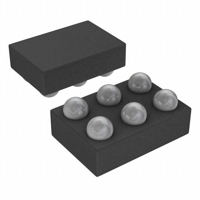
The MAX40100 is a low-power, zero-drift operational amplifier available in a space-saving, 6-bump, wafer-level
package (WLP).
● Low 66μA Quiescent Current
● Low Input Noise:
• 42nV/√Hz at 1kHz
• 0.42μVP-P from 0.1Hz to 10Hz
Designed for use in portable consumer, medical, and industrial applications, the MAX40100 features rail-to-rail
CMOS inputs and outputs, a 1.5MHz GBW at just 66μA
supply current, and 10μV (max) “zero-drift” input voltage
offset over time and temperature.
The zero-drift feature of the MAX40100 reduces the high
1/f noise typically found in CMOS input operational amplifiers, making it useful for a wide variety of low-frequency
measurement applications.
●
●
●
●
●
●
●
Rail-to-Rail Inputs and Outputs (RRIO)
1.5MHz GBW
Ultra-Low 10pA Input Bias Current
Single 1.6V to 5.5V Supply Voltage Range
Unity Gain Stable
Power-Saving Shutdown Mode
Tiny, 1.1mm x 0.76mm, 6-bump WLP
Ordering Information appears at end of data sheet.
The MAX40100 is available in a space-saving, 1.1 x
0.76mm, 6-bump WLP with 0.35mm bump pitch.
The MAX40100 is specified over the -40°C to +125°C extended automotive operating temperature range.
Applications
●
●
●
●
●
Cell Phones
Sensor Interfaces
Loop-Powered Systems
Portable Medical Devices
Battery-Powered Devices
Typical Application Circuit
VCC = 1.8V TO 5.5V
MAX40100
VIN+
VIN-
MAX40100
VOUT
R1
R2
R3
R4
HIGH INPUT IMPEDANCE 2-OP AMP INSTRUMENTATION AMPLIFIER
IF R1 = R4, R2 = R3, VOUT = (VIN+ - VIN-) X (1 + R4/R3)
R1, R2, R3, R4 ARE LOWER TOLERANCE (0.01%) FOR BETTER CMRR PERFORMANCE
19-8539; Rev 5; 2/21
�MAX40100
Precision, Low-Power and Low-Noise Op Amp with
RRIO
Absolute Maximum Ratings
IN+, IN-, Supply Voltage, SHDN (VDD to GND) ....... -0.3V to +6V
OUT ................................................(GND - 0.3V) to (VDD + 0.3V)
Short-Circuit Duration to Either Supply Rail,
OUT, OUTA, OUTB .............................................................10s
Continuous Input Current (Any Pins)................................. ±20mA
Continuous Power Dissipation (TA = +70°C)................................
6-Bump WLP (Derate 10.19mW/°C above +70°C)........... 816mW
Package Thermal Characteristics (multilayer board)
Junction-to-Ambient Thermal Resistance (θJA) ...... 98.06°C/W
Operating Temperature Range ...........................-40°C to +125°C
Junction Temperature ....................................................... +150°C
Storage Temperature Range .............................. -65ºC to +150ºC
Lead Temperature (soldering 10s).................................... +300ºC
Note 1: Package thermal resistances were obtained using the method described in JEDEC specification JESD51-7, using a four-layer
board. For detailed information on package thermal considerations, refer to www.maximintegrated.com/thermal-tutorial.
Stresses beyond those listed under “Absolute Maximum Ratings” may cause permanent damage to the device. These are stress ratings only, and functional operation of the
device at these or any other conditions beyond those indicated in the operational sections of the specifications is not implied. Exposure to absolute maximum rating conditions for
extended periods may affect device reliability.
Package Information
6 WLP
Package Code
N60D1+1
Outline Number
21-100086
Land Pattern Number
Refer to Application Note 1891
For the latest package outline information and land patterns (footprints), go to www.maximintegrated.com/packages.
Note that a “+”, “#”, or “-” in the package code indicates RoHS status only. Package drawings may show a different
suffix character, but the drawing pertains to the package regardless of RoHS status.
Package thermal resistances were obtained using the method described in JEDEC specification JESD51-7, using a
four-layer board. For detailed information on package thermal considerations, refer to www.maximintegrated.com/
thermal-tutorial.
www.maximintegrated.com
Maxim Integrated | 2
�MAX40100
Precision, Low-Power and Low-Noise Op Amp with
RRIO
Package Outline Drawing
www.maximintegrated.com
Maxim Integrated | 3
�MAX40100
Precision, Low-Power and Low-Noise Op Amp with
RRIO
Electrical Characteristics
(VDD = +3.3V, GND = 0, AV = 1V/V, VOUT = VDD/2, CL = 20pF, RL = 100kΩ to VDD/2, VSHDN = VDD, TA = -40°C to +125°C unless
otherwise noted. Typical values are at +25°C) (Note 2)
PARAMETER
SYMBOL
CONDITIONS
MIN
TYP
MAX
Guaranteed by PSRR, 0°C ≤ TA ≤ +70°C
1.6
5.5
Guaranteed by PSRR, -40°C ≤ TA ≤
+125°C
1.8
5.5
UNITS
POWER SUPPLY
Supply Voltage Range
VDD
Quiescent Supply
Current
IDD
Power-Supply Rejection
Ratio
PSRR
TA = +25°C
66
-40°C ≤ TA ≤ +125°C
VDD = 1.8V to 5.5V
124
TA = +25°C
116
-40°C ≤ TA ≤
+125°C
107
0°C ≤ TA ≤ +70°C, VDD = 1.6V to 5.5V
Power-Up Time
tON
Shutdown Supply
Current
ISHDN
Turn-On Time from
Shutdown
tOSD
92
V
μA
135
dB
107
VDD = 0 to 3V step, AV = 1V/V
20
μs
300
VDD = 3.3V, VSHDN = 0 to 3.3V step in <
1μs
50
TA = +25°C
0.8
nA
μs
DC SPECIFICATIONS
Input Offset Voltage
Input Offset Voltage Drift
Input Bias Current (Note
3)
Input Offset Current
Input Common-Mode
Range
Common-Mode
Rejection Ratio
Open-Loop Gain
Input Resistance
www.maximintegrated.com
VOS
-40°C ≤ TA ≤ +125°C
25
∆VOS
5
TA = +25°C
IB
±0.031
CMRR
AVOL
RIN
nV/°C
±4.6
-40°C ≤ TA ≤ +125°C
±28
±0.005
Guaranteed by
CMRR test
TA = +25°C
-0.1
-40°C ≤ TA ≤
+125°C
-0.1
VDD +
0.05
122
-0.1 ≤ VCM ≤ VDD + 0.05,
-40°C ≤ TA ≤ +125°C
116
20mV ≤ VOUT ≤ VDD - 20mV,
RL = 100kΩ to VDD/2
120
150mV ≤ VOUT ≤ VDD - 150mV,
RL = 5kΩ to VDD/2
123
nA
nA
VDD +
0.1
-0.1 ≤ VCM ≤ VDD + 0.1, TA = +25°C
μV
±0.160
-40°C ≤ TA ≤ +85°C
IOS
VCM
10
V
135
dB
138
dB
160
Differential
50
Common-mode
200
MΩ
Maxim Integrated | 4
�MAX40100
Precision, Low-Power and Low-Noise Op Amp with
RRIO
Electrical Characteristics (continued)
(VDD = +3.3V, GND = 0, AV = 1V/V, VOUT = VDD/2, CL = 20pF, RL = 100kΩ to VDD/2, VSHDN = VDD, TA = -40°C to +125°C unless
otherwise noted. Typical values are at +25°C) (Note 2)
PARAMETER
SYMBOL
VOH
CONDITIONS
VDD - VOUT
MIN
VOL
VOUT
RL = 50kΩ to
VDD/2
22
UNITS
50
mV
RL = 100kΩ to
VDD/2
11
RL = 50kΩ to
VDD/2
18
RL = 600Ω to
VDD/2
Short-Circuit Current
MAX
12
RL = 600Ω to
VDD/2
Output Voltage Swing
TYP
RL = 100kΩ to
VDD/2
50
ISC
50
mA
AC SPECIFICATIONS
Gain-Bandwidth Product
1.5
MHz
Slew Rate
GBWP
SR
0 ≤ VOUT ≤ 2V
0.7
V/µs
Input Voltage Noise
Density
En
fSW = 1kHz
42
nV/√Hz
Input Voltage Noise
0.1Hz ≤ fSW ≤ 10Hz
0.42
μVP-P
Input Current Noise
Density
fSW = 1kHz
100
fA/√Hz
Phase Margin
CL = 20pF
60
°
No sustained oscillation, AV = 1V/V
400
pF
Capacitive Loading
CL
LOGIC INPUT
Shutdown Input Low
VIL
Shutdown Input High
VIH
Shutdown Input
Leakage Current
IIL/IIH
0.5
1.3
V
V
100
nA
Note 2: Specifications are 100% tested at TA = +25°C (exceptions noted). All temperature limits are guaranteed by design.
Note 3: Guaranteed by design.
www.maximintegrated.com
Maxim Integrated | 5
�MAX40100
Precision, Low-Power and Low-Noise Op Amp with
RRIO
Typical Operating Characteristics
(VDD = +3.3V, GND = 0, AV = 1V/V, VOUT = VDD/2, CL = 20pF, RL = 100kΩ to VDD/2, VSHDN = VDD, TA = -40°C to +125°C unless
otherwise noted. Typical values are at +25°C)
www.maximintegrated.com
Maxim Integrated | 6
�MAX40100
Precision, Low-Power and Low-Noise Op Amp with
RRIO
Typical Operating Characteristics (continued)
(VDD = +3.3V, GND = 0, AV = 1V/V, VOUT = VDD/2, CL = 20pF, RL = 100kΩ to VDD/2, VSHDN = VDD, TA = -40°C to +125°C unless
otherwise noted. Typical values are at +25°C)
140
A C PSRR v s . FREQUENCY
toc10
120
AC PSRR (dB)
100
80
60
40
20
0
0.0001 0.001 0.01
0.1
1
10
100 1000 10000
INPUT FREQUENCY (kHz)
OPEN-L OOP GA IN v s . FREQUENCY
toc14
160
OPEN-LOOP GAIN (dB)
140
120
100
80
60
40
20
0
-20
0.001
0.1
10
1000
100000 10000000
INPUT FREQUENCY (Hz)
www.maximintegrated.com
Maxim Integrated | 7
�MAX40100
Precision, Low-Power and Low-Noise Op Amp with
RRIO
Typical Operating Characteristics (continued)
(VDD = +3.3V, GND = 0, AV = 1V/V, VOUT = VDD/2, CL = 20pF, RL = 100kΩ to VDD/2, VSHDN = VDD, TA = -40°C to +125°C unless
otherwise noted. Typical values are at +25°C)
Bump Configuration
TOP VIEW
MAX40100
2
3
A
VSS
VDD
SHDN
B
IN+
IN-
OUT
+
1
WLP
Bump Descriptions
PIN
NAME
FUNCTION
A1
VSS
Negative Supply Voltage
A2
VDD
Positive Supply Voltage. Bypass to GND with a 0.1μF capacitor.
A3
SHDN
www.maximintegrated.com
Shutdown. Pull to VSS to activate shutdown mode.
Maxim Integrated | 8
�MAX40100
Precision, Low-Power and Low-Noise Op Amp with
RRIO
Bump Descriptions (continued)
PIN
NAME
B1
IN+
Positive Input
B2
IN-
Negative Input
B3
OUT
www.maximintegrated.com
FUNCTION
Output
Maxim Integrated | 9
�MAX40100
Precision, Low-Power and Low-Noise Op Amp with
RRIO
Detailed Description
The MAX40100 is a precision, low-power op-amps ideal for signal processing applications. This device use an innovative
auto-zero technique that allows precision and low-noise with a minimum amount of power. The low input offset voltage,
CMOS inputs, and the absence of 1/f noise allows for optimization of active-filter designs.
The MAX40100 achieves rail-to-rail performance at the input through the use of a low-noise charge pump. This ensures
a glitch-free, common-mode input voltage range extending from the negative supply rail up to the positive supply
rail, eliminating cross over distortion common to traditional N-channel/P-channel CMOS pair inputs, reducing harmonic
distortion at the output.
The device features a shutdown mode that greatly reduces quiescent current while the device is not operational.
Auto-Zero
The MAX40100 features an auto-zero circuit that allows the device to achieve less than 10μV of input offset voltage and
eliminates the 1/f noise.
Internal Charge Pump
An internal charge pump provides an internal supply typically 1V beyond the upper rail. This internal rail allows the
MAX40100 to achieve true rail-to-rail inputs and outputs, while providing excellent common-mode rejection, powersupply rejection ratios, and gain linearity.
The charge pump requires no external components, and in most applications is entirely transparent to the user. The
operating frequency is well beyond the unity-gain frequency of the amplifier, avoiding aliasing or other signal integrity
issues in sensitive applications.
Shutdown Operation
The device features an active-low shutdown mode that lowers the quiescent current to less than 1µA. In shutdown mode
the inputs and output are high impedance. This allows multiple devices to be multiplexed onto a single line without the
use of external buffers. Pull SHDN high for normal operation.
The shutdown high (VIH) and low (VIL) threshold voltages are designed for ease of integration with digital controls like
microcontroller outputs. These thresholds are independent of supply, eliminating the need for external pulldown circuitry.
www.maximintegrated.com
Maxim Integrated | 10
�MAX40100
Precision, Low-Power and Low-Noise Op Amp with
RRIO
Applications Information
The MAX40100 is a low-power, low-noise, precision operational amplifier designed for applications in the portable
medical (such as ECG and Pulse Oximetry), portable consumer, and industrial markets.
The MAX40100 is also ideal for loop-powered systems that interface with pressure sensors or strain-gauges.
Capacitive Load Stability
Driving large capacitive loads can cause instability in many op amps. MAX40100 is stable with capacitive loads up
to 400pF. Stability with higher capacitive loads can be improved by adding an isolation resistor in series with the opamp output. This resistor improves the circuit’s phase margin by isolating the load capacitor from the amplifier’s output.
The graph in the Typical Operating Characteristics gives the stable operation region for capacitive load versus isolation
resistors.
Power Supplies and Layout
The MAX40100 operate either with a single supply from +1.6V to +5.5V with respect to ground or with dual supplies from
±0.8V to ±2.75V. When used with dual supplies, bypass both supplies with their own 0.1μF capacitor to ground. When
used with a single supply, bypass VDD with a 0.1μF capacitor to ground.
Careful layout technique helps optimize performance by decreasing the amount of stray capacitance at the op amp’s
inputs and outputs. To decrease stray capacitance, minimize trace lengths by placing external components close to the
op amp’s pins.
Typical Application Circuit
VCC = 1.8V TO 5.5V
MAX40100
VIN+
VIN-
MAX40100
VOUT
R1
R2
R3
R4
HIGH INPUT IMPEDANCE 2-OP AMP INSTRUMENTATION AMPLIFIER
IF R1 = R4, R2 = R3, VOUT = (VIN+ - VIN-) X (1 + R4/R3)
R1, R2, R3, R4 ARE LOWER TOLERANCE (0.01%) FOR BETTER CMRR PERFORMANCE
Ordering Information
PART
MAX40100ANT+
TEMP RANGE
PIN-PACKAGE
-40°C to +125°C
6 WLP
+Denotes lead(Pb)-free/RoHS compliant package.
www.maximintegrated.com
Maxim Integrated | 11
�MAX40100
Precision, Low-Power and Low-Noise Op Amp with
RRIO
Revision History
REVISION
NUMBER
REVISION
DATE
0
5/16
Initial release
1
6/17
Updated units in Electrical Characteristics table
2
3/18
Updated Absolute Maximum Ratings sections
2
3
3/20
Updated TOC02
4
4
1/21
Updated Benefits and Features, added Package Outline Drawing
5
2/21
Added Typical Application Circuit
DESCRIPTION
PAGES
CHANGED
—
2, 3
1, 3
1
For pricing, delivery, and ordering information, please visit Maxim Integrated’s online storefront at https://www.maximintegrated.com/en/storefront/storefront.html.
Maxim Integrated cannot assume responsibility for use of any circuitry other than circuitry entirely embodied in a Maxim Integrated product. No circuit patent
licenses are implied. Maxim Integrated reserves the right to change the circuitry and specifications without notice at any time. The parametric values (min and max
limits) shown in the Electrical Characteristics table are guaranteed. Other parametric values quoted in this data sheet are provided for guidance.
Maxim Integrated and the Maxim Integrated logo are trademarks of Maxim Integrated Products, Inc.
© 2021 Maxim Integrated Products, Inc.
�


 工商网监
湘ICP备2023018690号
工商网监
湘ICP备2023018690号
