19-1221; Rev 3; 8/01
Single/Dual/Quad, 270MHz, 1mA, SOT23,
Current-Feedback Amplifiers with Shutdown
The MAX4180–MAX4187 feature 0.08%/0.03° differential gain and phase errors, a 20ns settling time to 0.1%,
and a 450V/µs slew rate, making them ideal for highperformance video applications. The MAX4180/
MAX4181/MAX4183/MAX4185 have a low-power shutdown mode that reduces power-supply current to 135µA
and places the outputs in a high-impedance state. This
feature makes them ideal for multiplexing applications.
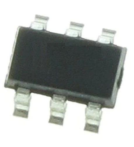
The single MAX4180/MAX4181 are offered in spacesaving 6-pin SOT23 packages.
Features
♦ Ultra-Low Supply Current: 1mA per Amplifier
♦ Shutdown Mode
Outputs Placed in High-Z
Supply Current Reduced to 135µA
♦ Operate from a Single +5V Supply or
Dual ±5V Supplies
♦ Wide Bandwidth
270MHz -3dB Small-Signal Bandwidth
(MAX4181/MAX4184/MAX4185/MAX4187)
♦ 450V/µs Slew Rate
♦ Fast, 20ns Settling Time to 0.1%
♦ Excellent Video Specifications
Gain Flatness to 70MHz
(MAX4180/MAX4182/MAX4183/MAX4186)
0.08%/0.03° Differential Gain/Phase
♦ Low Distortion:
-73dBc SFDR (fC = 5MHz, VOUT = 2Vp-p)
♦ Available in Tiny Surface-Mount Packages
6-Pin SOT23 (MAX4180/MAX4181)
10-Pin µMAX (MAX4183/MAX4185)
16-Pin QSOP (MAX4186/MAX4187)
Ordering Information
________________________Applications
Portable/Battery-Powered
Video/Multimedia Systems
High-Definition
Surveillance Video
Broadcast and High-Definition
TV Systems
Professional
Cameras
High-Speed A/D Buffers
CCD Imaging Systems
Video Switching/
Multiplexing
PART
TEMP
RANGE
PINPACKAGE
TOP
MARK
MAX4180EUT-T
-40°C to +85°C
6 SOT23-6
AAAB
MAX4180ESA
-40°C to +85°C
8 SO
Pin Configurations
Medical Imaging
Selector Guide
NO. OF
AMPS
SHUTDOWN
MODE
OPTIMIZED
FOR
MAX4180
1
Yes
AV ≥ 2
MAX4181
1
Yes
AV ≥ 1
MAX4182
2
No
AV ≥ 2
MAX4183
2
Yes
AV ≥ 2
MAX4184
2
No
AV ≥ 1
MAX4185
2
Yes
AV ≥ 1
MAX4186
4
No
AV ≥ 2
MAX4187
4
No
AV ≥ 1
PART
—
Ordering Information continued at end of data sheet.
TOP VIEW
SINGLE
OUT 1
VEE 2
MAX4180
MAX4181
IN+ 3
6
VCC
5
SHDN
4
IN-
SOT23-6
Pin Configurations continued at end of data sheet.
________________________________________________________________ Maxim Integrated Products
For pricing, delivery, and ordering information, please contact Maxim/Dallas Direct! at
1-888-629-4642, or visit Maxim’s website at www.maxim-ic.com.
1
MAX4180–MAX4187
General Description
The MAX4180 family of current-feedback amplifiers
combines high-speed performance, low distortion,
and excellent video specifications with ultra-low-power
operation in miniature packages. They operate from
±2.25V to ±5.5V dual supplies, or from a single +5V
supply. They require only 1mA of supply current per amplifier while delivering up to ±60mA of output current
drive. The MAX4180/MAX4182/MAX4183/MAX4186
are compensated for applications with a closed-loop
gain of +2 (6dB) or greater, and provide a -3dB bandwidth of 240MHz and a 0.1dB bandwidth of 70MHz.
The MAX4181/MAX4184/MAX4185/MAX4187 are compensated for applications with a +1 (0dB) or greater
gain, and provide a -3dB bandwidth of 270MHz and a
0.1dB bandwidth of 60MHz.
�MAX4180–MAX4187
Single/Dual/Quad, 270MHz, 1mA, SOT23,
Current-Feedback Amplifiers with Shutdown
ABSOLUTE MAXIMUM RATINGS
Supply Voltage (VCC to VEE) .................................................12V
Analog Input Voltage.......................(VEE - 0.3V) to (VCC + 0.3V)
Differential Input Voltage.......................................................±2V
SHDN Input Voltage ........................(VEE - 0.3V) to (VCC + 0.3V)
Short-Circuit Duration (OUT to GND, VCC or VEE).....Continuous
Continuous Power Dissipation (TA = +70°C)
6-Pin SOT23 (derate 7.10mW/°C above +70°C)...........571mW
8-Pin SO (derate 5.88mW/°C above +70°C).................471mW
10-Pin µMAX (derate 5.60mW/°C above +70°C) ..........444mW
14-Pin SO (derate 8.33mW/°C above +70°C)...............667mW
16-Pin QSOP (derate 8.30mW/°C above +70°C)..........667mW
Operating Temperature Range ...........................-40°C to +85°C
Storage Temperature Range .............................-65°C to +150°C
Lead Temperature (soldering, 10s) .................................+300°C
Stresses beyond those listed under “Absolute Maximum Ratings” may cause permanent damage to the device. These are stress ratings only, and functional
operation of the device at these or any other conditions beyond those indicated in the operational sections of the specifications is not implied. Exposure to
absolute maximum rating conditions for extended periods may affect device reliability.
DC ELECTRICAL CHARACTERISTICS—Dual Supplies
(VCC = +5V, VEE = -5V, VIN+ = 0, SHDN ≥ 3V; TA = TMIN to TMAX, unless otherwise noted. Typical values are at TA = +25°C.) (Note 1)
PARAMETER
Input Voltage Range
Input Offset Voltage
Input Offset-Voltage Drift
SYMBOL
CONDITIONS
VCM
Guaranteed by CMRR test
VOS
VCM = 0
MIN
TYP
±3.6
±3.9
±1.5
TCVOS
Input Offset-Voltage Matching
MAX4182–MAX4187
MAX
UNITS
V
±7
mV
±12
µV/°C
±1
mV
Input Bias Current
(Positive Input)
IB+
±1
±7
µA
Input Bias Current
(Negative Input)
IB-
±1
±12
µA
Input Resistance
(Positive Input)
RIN+
Input Resistance
(Negative Input)
RIN-
Common-Mode Rejection Ratio
Open-Loop Transresistance
CMRR
TR
Output Voltage Swing
VSW
Output Current
IOUT
-3.6V ≤ VIN+ ≤ 3.6V, -1V ≤ (VIN+ - VIN-) ≤ 1V
250
Output Resistance
Disabled Output Leakage
Current
160
Ω
dB
-50
-58
RL = 1kΩ, VOUT = ±3.6V
0.8
3.0
RL = 150Ω, VOUT = ±2.5V
0.3
0.9
RL = 1kΩ
±3.75
±4.0
RL = 150Ω
±3.0
±3.3
MΩ
V
±3.0
±60
mA
ISC
±80
mA
ROUT
0.2
Ω
IOUT(OFF)
RL = 30Ω
±32
SHDN ≤ VIL, VOUT ≤ ±3V (Notes 2, 4)
SHDN Logic Low Threshold
VIL
(Notes 3, 4)
SHDN Logic High Threshold
VIH
(Notes 3, 4)
2
kΩ
-3.6V ≤ VCM ≤ 3.6V
RL = 100Ω
Output Short-Circuit Current
800
±0.1
±6.0
µA
VCC - 3.0
V
VCC - 2.0
_______________________________________________________________________________________
V
TOP VIEW
SING
OUT 1
�Single/Dual/Quad, 270MHz, 1mA, SOT23,
Current-Feedback Amplifiers with Shutdown
(VCC = +5V, VEE = -5V, VIN+ = 0, SHDN ≥ 3V; TA = TMIN to TMAX, unless otherwise noted. Typical values are at TA = +25°C.) (Note 1)
PARAMETER
SYMBOL
SHDN Logic Input Bias Current
IIN
CONDITIONS
MIN
VEE ≤ SHDN ≤ VCC (Note 4)
TYP
MAX
UNITS
±0.1
±2.0
µA
Positive Power-Supply
Rejection Ratio
PSRR+
VEE = -5V, VCC = 4.5V to 5.5V
60
71
dB
Negative Power-Supply
Rejection Ratio
PSRR-
VCC = 5V, VEE = -4.5V to -5.5V
53
62
dB
Operating Supply Voltage
VCC/VEE
Quiescent Supply Current
per Amplifier
IS
Shutdown Supply Current
per Amplifier
IS(OFF)
±2.25
RL = ∞
±5.50
MAX418_EUT
1.0
1.3
All other packages
1.0
1.2
135
180
SHDN = 0, RL = ∞ (Note 4)
V
mA
µA
DC ELECTRICAL CHARACTERISTICS—Single Supply
(VCC = +5V, VEE = 0, VIN+ = 2.5V, SHDN ≥ 3V, RL to VCC/2; TA = TMIN to TMAX, unless otherwise noted. Typical values are at
TA = +25°C.) (Note 1)
PARAMETER
Input Voltage Range
Input Offset Voltage
Input Offset Voltage Drift
SYMBOL
CONDITIONS
VCM
VOS
MIN
TYP
1.3 to
3.7
1.1 to
3.9
VCM = 2.5V
±1.5
TCVOS
Input Offset Voltage Matching
MAX4182–MAX4187
MAX
UNITS
V
±7
mV
±12
µV/°C
±1
mV
Input Bias Current
(Positive Input)
IB+
±1
±7
µA
Input Bias Current
(Negative Input)
IB-
±1
±12
µA
Input Resistance
(Positive Input)
RIN+
Input Resistance
(Negative Input)
RIN-
Common-Mode
Rejection Ratio
CMRR
Open-Loop
Transresistance
TR
1.3V ≤ VIN+ ≤ 3.7V, -1V ≤ (VIN+ - VIN-) ≤ 1V
800
kΩ
160
Ω
-50
-58
dB
RL = 1kΩ, VOUT = 1.2V to 3.8V
0.8
2.5
RL = 150Ω, VOUT = 1.4V to 3.6V
0.275
0.9
1.15 to
3.85
1.35 to
3.65
1.0 to
4.0
1.2 to
3.8
1.3 to
3.7
1.3V ≤ VCM ≤ 3.7V
RL = 1kΩ
Output Voltage Swing
VSW
RL = 150Ω
RL = 100Ω
250
MΩ
V
V
_______________________________________________________________________________________
3
MAX4180–MAX4187
DC ELECTRICAL CHARACTERISTICS—Dual Supplies (continued)
�MAX4180–MAX4187
Single/Dual/Quad, 270MHz, 1mA, SOT23,
Current-Feedback Amplifiers with Shutdown
DC ELECTRICAL CHARACTERISTICS—Single Supply (continued)
(VCC = +5V, VEE = 0, VIN+ = 2.5V, SHDN ≥ 3V, RL to VCC/2; TA = TMIN to TMAX, unless otherwise noted. Typical values are at
TA = +25°C.) (Note 1)
PARAMETER
Output Current
Output Short-Circuit Current
Output Resistance
Disabled Output
Leakage Current
SYMBOL
MIN
TYP
±18
±30
mA
ISC
±50
mA
ROUT
0.2
Ω
IOUT
IOUT(OFF)
CONDITIONS
RL = 30Ω
SHDN ≤ VIL, 1.2V ≤ VOUT ≤ 3.8V
(Notes 2, 4)
SHDN Logic-Low Threshold
VIL
(Notes 3, 4)
SHDN Logic-High Threshold
VIH
(Notes 3, 4)
SHDN Logic Input Bias Current
IIN
0 ≤ SHDN ≤ VCC (Note 4)
Power-Supply Rejection Ratio
Operating Supply Voltage
PSRR
IS
Shutdown Supply Current
per Amplifier
IS(OFF)
µA
VCC 3.0
V
V
±0.1
VCC = 4.5V to 5.5V
60
±2.0
71
4.5
RL = ∞
µA
dB
5.5
MAX418_EUT
1.0
1.25
All other packages
1.0
1.2
135
180
SHDN = 0, RL = ∞ (Note 4)
UNITS
±4.0
VCC 2.0
VCC
Quiescent Supply Current
per Amplifier
±0.1
MAX
V
mA
µA
AC ELECTRICAL CHARACTERISTICS—Dual Supplies (MAX4180/4182/4183/4186)
(VCC = +5V, VEE = -5V, VIN = 0, SHDN ≥ 3V, AV = +2V/V; see Table 1 for RF and RG values; TA = +25°C, unless otherwise noted.)
PARAMETER
SYMBOL
CONDITIONS
Small-Signal -3dB Bandwidth
(Note 5)
BWSS