19-2279; Rev 4; 3/06
SOT23, 3V/5V, Single-Supply, Rail-to-Rail
Instrumentation Amplifiers
The MAX4460/MAX4461/MAX4462 are instrumentation
amplifiers with precision specifications, low-power consumption, and excellent gain-bandwidth product.
Proprietary design techniques allow ground-sensing
capability combined with ultra-low input current and
increased common-mode rejection performance. These
rail-to-rail output instrumentation amplifiers are offered in
fixed or adjustable gains and the option for either a shutdown mode or a pin to set the output voltage relative to
an external reference (see the Ordering Information and
Selector Guide).
The MAX4460 has an adjustable gain and uses ground
as its reference voltage. The MAX4461 is offered in fixed
gains of 1, 10, and 100, uses ground as its reference voltage, and has a logic-controlled shutdown input. The
MAX4462 is offered in fixed gains of 1, 10, and 100 and
has a reference input pin (REF). REF sets the output voltage for zero differential input to allow bipolar signals in
single-supply applications.
The MAX4460/MAX4461/MAX4462 have high-impedance
inputs optimized for small-signal differential voltages. The
MAX4461/MAX4462 are factory trimmed to gains of 1, 10,
or 100 (suffixed U, T, and H) with ±0.1% accuracy. The
typical offset of the MAX4460/MAX4461/MAX4462 is
100µV. All devices have a gain-bandwidth product of
2.5MHz.
These amplifiers operate with a single-supply voltage
from 2.85V to 5.25V and with a quiescent current of only
700µA (less than 1µA in shutdown for the MAX4461). The
MAX4462 can also be operated with dual supplies.
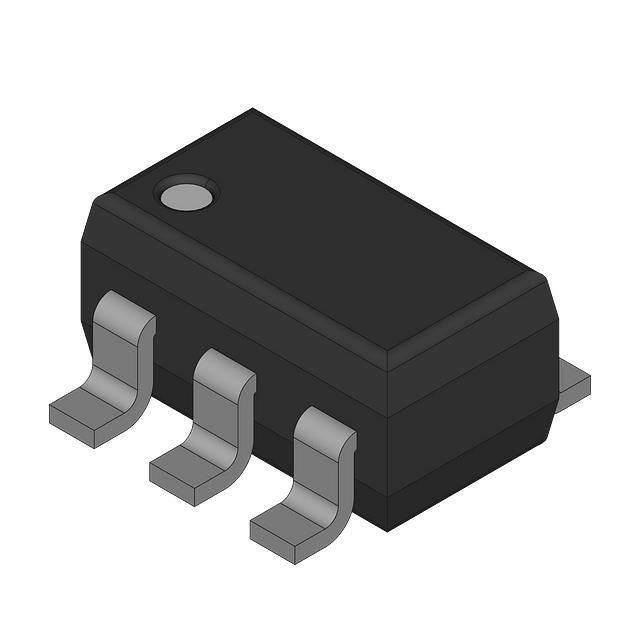
Smaller than most competitors, the MAX4460/
MAX4461/MAX4462 are available in space-saving 6-pin
SOT23 and TDFN packages.
________________________Applications
Industrial Process Control
Strain-Gauge Amplifiers
Transducer Interface
Features
♦
♦
♦
♦
♦
♦
♦
♦
♦
♦
Tiny 6-Pin SOT23 and TDFN Packages
Input Negative Rail Sensing
1pA (typ) Input Bias Current
100µV Input Offset Voltage
Rail-to-Rail Output
2.85V to 5.25V Single Supply
700µA Supply Current
±0.1% Gain Error
2.5MHz Gain-Bandwidth Product
18nV/√Hz Input-Referred Noise
Ordering Information
TEMP
RANGE
PINPACKAGE
TOP
MARK
MAX4460ETT+T
-40°C to +85°C
6 TDFN-EP*
+ANI
MAX4460EUT-T
-40°C to +85°C
6 SOT23-6
AASS
MAX4460ESA
-40°C to +85°C
8 SO
MAX4461UETT+T
-40°C to +85°C
6 TDFN-EP*
+ANJ
MAX4461UEUT-T
-40°C to +85°C
6 SOT23-6
AAST
MAX4461UESA
-40°C to +85°C
8 SO
MAX4461TETT+T
-40°C to +85°C
6 TDFN-EP*
+ANK
MAX4461TEUT-T
-40°C to +85°C
6 SOT23-6
AASU
MAX4461TESA
-40°C to +85°C
8 SO
MAX4461HETT+T
-40°C to +85°C
6 TDFN-EP*
+ANL
MAX4461HEUT-T
-40°C to +85°C
6 SOT23-6
AASV
MAX4461HESA
-40°C to +85°C
8 SO
PART
—
—
—
—
+Denotes lead-free package.
*EP = Exposed paddle.
Ordering Information continued at end of data sheet.
Typical Application Circuits
Precision Low-Side Current Sense
VCC
Low-Noise Microphone Preamplifier
Differential Voltage Amplification
Battery-Powered Medical Equipment
Selector Guide appears at end of data sheet.
VCM + ∆V
3
5
MAX4462
1
VCM - ∆V
OUT
6
4
2
REF
Pin Configurations appear at end of data sheet.
Typical Application Circuits continued at end of data sheet.
________________________________________________________________ Maxim Integrated Products
For pricing, delivery, and ordering information, please contact Maxim/Dallas Direct! at
1-888-629-4642, or visit Maxim’s website at www.maxim-ic.com.
1
MAX4460/MAX4461/MAX4462
General Description
�MAX4460/MAX4461/MAX4462
SOT23, 3V/5V, Single-Supply, Rail-to-Rail
Instrumentation Amplifiers
ABSOLUTE MAXIMUM RATINGS
Supply Voltage (VDD to VSS) ...................................-0.3V to +6V
All Other Pins ...................................(VSS - 0.3V) to (VDD + 0.3V)
Output Short-Circuit Duration to Either Supply.........................1s
Continuous Power Dissipation (TA = +70°C)
6-Pin SOT23 (derate 8.7mW/°C above +70°C)............695mW
6-Pin TDFN-EP (derate 18.2mW/°C above +70°C) ....1454mW
8-Pin SO (derate 5.9mW/°C above +70°C)..................470mW
Operating Temperature Range ...........................-40°C to +85°C
Junction Temperature ......................................................+150°C
Storage Temperature Range .............................-65°C to +150°C
Lead Temperature (soldering, 10s)....................................300°C
Stresses beyond those listed under “Absolute Maximum Ratings” may cause permanent damage to the device. These are stress ratings only, and functional
operation of the device at these or any other conditions beyond those indicated in the operational sections of the specifications is not implied. Exposure to
absolute maximum rating conditions for extended periods may affect device reliability.
ELECTRICAL CHARACTERISTICS—MAX4460/MAX4461
(VDD = 5V, VCM = 0V, VDIFF = VIN+ - VIN- = 50mV to 100mV for G = 1, 20mV to 100mV for G = 10, 2mV to 48mV for G =100,
MAX4460 is configured for G = 10, RL = 200kΩ to GND, TA = +25°C, unless otherwise noted.)
PARAMETER
Supply Voltage
SYMBOL
VDD
Supply Current
CONDITIONS
Guaranteed by PSRR test
VOS
0.68
0.9
VDD = 5V
0.1
1
±50
±425
MAX4461ESA
±50
±300
MAX446_EUT/MAX446_ETT
±100
±600
Differential mode
2
Common mode
2
VCM = VDD/2
Input Common-Mode Range
VCM
Guaranteed by CMRR test
-0.1
Input Common-Mode
Rejection Ratio
CMRR
VCM = -0.1V to (VDD - 1.7V)
90
120
Power-Supply Rejection Ratio
PSRR
VDD = 2.85V to 5.25V
80
100
FB Input Current
VOL
Short-Circuit Current
2
ISC
VDD 1.7
V
dB
dB
pA
1
100
pA
MAX4461
Output Voltage Swing
GΩ
MAX4460 (Note 2)
VIL
VOH
µV
100
MAX4461
en
µA
1
0.7 X
VDD
SHDN Logic Levels
Input Voltage Noise
mA
(Note 2)
VIH
SHDN Input Current
V
VDD = 3V, VDIFF = 0V
RIN
IB
UNITS
5.25
1.1
Input Resistance
Input Bias Current
MAX
0.80
MAX4460ESA
Input Offset Voltage (Note 1)
TYP
VDD = 5V, VDIFF = 0V
MAX4461, SHDN = GND
Shutdown Supply Current
MIN
2.85
V
0.3 X
VDD
MAX4461, V SHDN = 0V or VDD (Note 2)
1
f = 10kHz
18
f = 1kHz
38
VDD - VOH (Note 3)
RL = 200kΩ
RL = 20kΩ
(Note 4)
100
nV/√Hz
RL = 200kΩ
1
2.5
RL = 20kΩ
3
5
0
0.2
0
0.2
±150
_______________________________________________________________________________________
pA
mV
mA
�SOT23, 3V/5V, Single-Supply, Rail-to-Rail
Instrumentation Amplifiers
(VDD = 5V, VCM = 0V, VDIFF = VIN+ - VIN- = 50mV to 100mV for G = 1, 20mV to 100mV for G = 10, 2mV to 48mV for G =100,
MAX4460 is configured for G = 10, RL = 200kΩ to GND, TA = +25°C, unless otherwise noted.)
PARAMETER
SYMBOL
CONDITIONS
MIN
TYP
MAX
0.1
0.3
G = 10V/V, MAX4461TESA
0.12
0.35
G = 100V/V, MAX4461HESA
0.15
0.6
G = 10V/V, MAX4460ESA
0.15
0.35
G = 1V/V, MAX4461UESA
Gain Error
RL = 20kΩ
MAX446_EUT/MAX446_ETT
Nonlinearity (Note 1)
Maximum Capacitive Load
-3dB Bandwidth
CL
BW-3dB
Gain-Bandwidth Product
Slew Rate
GBWP
SR
0.15
0.6
RL = 20kΩ
0.05
0.15
No sustained oscillations
100
CL = 100pF
G = 1V/V, MAX4461U
2500
G = 10V/V, MAX4461T
250
G = 100V/V, MAX4461H
25
CL = 100pF
CL = 100pF
0.5
G = 10V/V
0.5
G = 100V/V
0.25
G = 1V/V
Settling Time
tS
%
%
pF
kHz
2.5
G = 1V/V
UNITS
MHz
V/µs
15
CL = 100pF,
within 0.1% of G = 10V/V
final value
G = 100V/V
75
µs
250
ELECTRICAL CHARACTERISTICS—MAX4460/MAX4461
(VDD = 5V, VCM = 0V, VDIFF = VIN+ - VIN- = 50mV to 100mV for G = 1, 20mV to 100mV for G = 10, 2mV to 48mV for G = 100,
MAX4460 is configured for G = 10, RL = 200kΩ to GND, TA = TMIN to TMAX, unless otherwise noted.)
PARAMETER
Supply Voltage
SYMBOL
VDD
Supply Current
CONDITIONS
Guaranteed by PSRR test
VDD = 5V
V
1
TA = 0°C to +85°C
±750
TA = -40°C to +85°C
±950
MAX4461ESA
G=1
±750
G = 10
±500
G = 100
±500
G=1
±950
G = 10
±750
(Note 1)
mA
µA
µV
±750
G = 100
MAX446_EUT/
MAX446_ETT
TCVOS
5.25
1.15
TA = -40°C to
+85°C
Input Offset-Voltage Drift
UNITS
VDD = 3V, VDIFF = 0V
TA = 0°C to
+85°C
VOS
2.85
MAX
1.4
MAX4460ESA
Input Offset Voltage (Note 1)
TYP
VDD = 5V, VDIFF = 0V
MAX4461,
SHDN = GND
Shutdown Supply Current
MIN
TA = 0°C to +85°C
±1400
TA = -40°C to +85°C
±1900
1.5
µV/°C
_______________________________________________________________________________________
3
MAX4460/MAX4461/MAX4462
ELECTRICAL CHARACTERISTICS—MAX4460/MAX4461 (continued)
�MAX4460/MAX4461/MAX4462
SOT23, 3V/5V, Single-Supply, Rail-to-Rail
Instrumentation Amplifiers
ELECTRICAL CHARACTERISTICS—MAX4460/MAX4461 (continued)
(VDD = 5V, VCM = 0V, VDIFF = VIN+ - VIN- = 50mV to 100mV for G = 1, 20mV to 100mV for G = 10, 2mV to 48mV for G = 100,
MAX4460 is configured for G = 10, RL = 200kΩ to GND, TA = TMIN to TMAX, unless otherwise noted.)
PARAMETER
Input Common-Mode Range
SYMBOL
VCM
CONDITIONS
Guaranteed by CMRR test
MIN
-0.1
Input Common-Mode Rejection
Ratio
CMRR
VCM = -0.1V to (VDD - 1.85V)
80
Power-Supply Rejection Ratio
PSRR
VDD = 2.85V to 5.25V
75
Input Bias Current
IB
FB Input Current
(Note 2)
MAX4460 (Note 2)
VIH
MAX4461
VIL
MAX4461
VOH
VDD - VOH
(Note 3)
SHDN Input Current
VOL
4
V
dB
dB
100
pA
100
pA
V
100
4
RL = 20kΩ
8
0.25
RL = 20kΩ
pA
mV
0.25
TA = 0°C to +85°C
0.8
TA = -40°C to +85°C
1.6
TA = 0°C to +85°C
0.8
TA = -40°C to +85°C
1.7
TA = 0°C to +85°C
1.0
MAX4461TESA,
RL = 20kΩ
MAX4461HESA,
RL = 20kΩ
TA = -40°C to +85°C
2.0
TA = 0°C to +85°C
0.8
TA = -40°C to +85°C
2.0
MAX4460ESA,
RL = 20kΩ
Nonlinearity
VDD 1.85
RL = 200kΩ
RL = 200kΩ
MAX4461UESA,
RL = 20kΩ
UNITS
0.3 X
VDD
MAX4461, V SHDN = 0V or VDD (Note 2)
Output Voltage Swing
MAX
0.7 X
VDD
SHDN Logic Levels
Gain Error
TYP
MAX446_EUT/
MAX446_ETT,
RL = 20kΩ
TA = 0°C to +85°C
1.8
TA = -40°C to +85°C
3.0
RL = 20kΩ
(Note 1)
TA = 0°C to +85°C
0.20
TA = -40°C to +85°C
0.25
_______________________________________________________________________________________
%
%
�SOT23, 3V/5V, Single-Supply, Rail-to-Rail
Instrumentation Amplifiers
(VDD = 5V, VSS = 0V, VCM = VREF = VDD/2, RL = 100kΩ to VDD/2, TA = +25°C, unless otherwise noted. VDIFF = VIN+ - VIN- = -100mV
to +100mV for G = 1 and G = 10, -20mV to +20mV for G = 100.)
PARAMETER
Supply Voltage
SYMBOL
VDD
Supply Current
CONDITIONS
Guaranteed by PSRR test
MIN
TYP
2.85
MAX
UNITS
5.25
V
VDD = 5V, VDIFF = 0V
0.8
1.1
VDD = 3V, VDIFF = 0V
0.68
0.9
MAX4462_ESA
±50
±250
MAX4462_EUT/MAX4462_ETT
±100
±500
mA
Input Offset Voltage (Note 1)
VOS
Input Resistance
RIN
VCM = VDD/2
Input Common-Mode Range
VCM
Guaranteed by Input CMRR test
VSS 0.1
VDD 1.7
V
Guaranteed by REF rejection test
VSS +
0.1
VDD 1.7
V
VCM = (VSS - 0.1V) to (VDD - 1.7V)
90
120
dB
VCM = (VSS + 0.1V) to (VDD - 1.7V)
85
100
dB
VDD = 2.85V to 5.25V
80
100
dB
REF Input Range
Input Common-Mode
Rejection Ratio
CMRR
REF Input Rejection Ratio
Power-Supply Rejection Ratio
Input Bias Current
PSRR
IB
Input Voltage Noise
eN
VOH
Gain Error
Nonlinearity
2
Common mode
2
(Note 2)
1
f = 10kHz
18
f = 1kHz
38
VDD - VOH
(Note 3)
Output Voltage Swing
Short-Circuit Current
Differential mode
VOL
VOL - VSS
(Note 3)
ISC
(Note 4)
RL = 10kΩ
RL = 10kΩ
GΩ
100
pA
nV/√Hz
RL = 100kΩ
1
2.5
RL = 10kΩ
3
5
RL = 100kΩ
2
4
6
12
RL = 10kΩ
µV
±150
mV
mA
G = 1V/V, MAX4462UESA
0.1
0.30
G = 10V/V, MAX4462TESA
0.12
0.35
G = 100V/V, MAX4462HESA
0.15
0.5
MAX4462_EUT/MAX4462_ETT
0.15
0.5
0.05
0.15
%
%
_______________________________________________________________________________________
5
MAX4460/MAX4461/MAX4462
ELECTRICAL CHARACTERISTICS—MAX4462
�MAX4460/MAX4461/MAX4462
SOT23, 3V/5V, Single-Supply, Rail-to-Rail
Instrumentation Amplifiers
ELECTRICAL CHARACTERISTICS—MAX4462 (continued)
(VDD = 5V, VSS = 0V, VCM = VREF = VDD/2, RL = 100kΩ to VDD/2, TA = +25°C, unless otherwise noted. VDIFF = VIN+ - VIN- = -100mV
to +100mV for G = 1 and G = 10, -20mV to +20mV for G = 100.)
PARAMETER
Maximum Capacitive Load
-3dB Bandwidth
Gain-Bandwidth Product
Slew Rate
Settling Time
SYMBOL
CL
BW-3dB
GBWP
SR
tS
CONDITIONS
MIN
No sustained oscillations
CL = 100pF
TYP
MAX
100
G = 1V/V, MAX4462U
2500
G = 10V/V, MAX4462T
250
G = 100V/V, MAX4462H
25
CL = 100pF
pF
kHz
2.5
CL = 100pF
CL = 100pF,
within 0.1% of
final value
G = 1V/V, MAX4462U
0.5
G = 10V/V, MAX4462T
0.5
G = 100V/V, MAX4462H
0.25
G = 1V/V, MAX4462U
15
G = 10V/V, MAX4462T
75
G = 100V/V, MAX4462H
250
UNITS
MHz
V/µs
µs
ELECTRICAL CHARACTERISTICS—MAX4462
(V DD = 5V, V SS = 0V, V CM = V REF = V DD /2, R L = 100kΩ to V DD /2, T A = T MIN to T MAX , unless otherwise noted. V DIFF =
VIN+ - VIN- = -100mV to +100mV for G = 1 and G = 10, -20mV to +20mV for G = 100.) (Note 5)
PARAMETER
Supply Voltage
SYMBOL
VDD
Supply Current
CONDITIONS
Guaranteed by PSRR test
Input Offset Voltage Drift
Input Common-Mode Range
VOS
TCVOS
VCM
REF Input Range
Input Common-Mode
Rejection Ratio
CMRR
REF Input Rejection Ratio
Power-Supply Rejection Ratio
Input Bias Current
6
PSRR
IB
TYP
2.85
MAX
UNITS
5.25
V
VDD = 5V, VDIFF = 0V
1.4
VDD = 3V, VDIFF = 0V
1.15
MAX4462_ESA
Input Offset Voltage (Note 1)
MIN
MAX4462_EUT/
MAX4462_ETT
TA = 0°C to +85°C
±500
TA = -40°C to +85°C
±750
TA = 0°C to +85°C
±1100
TA = -40°C to +85°C
±1300
(Note 1)
1.5
mA
µV
µV/°C
Guaranteed by input CMRR test
VSS 0.1
VDD 1.85
V
Guaranteed by REF rejection test
VSS +
0.1
VDD 1.85
V
VCM = (VSS – 0.1V) to (VDD - 1.85V)
80
dB
VCM = (VSS + 0.1V) to (VDD - 1.85V)
75
dB
VDD = 2.85V to 5.25V
75
dB
(Note 2)
_______________________________________________________________________________________
100
pA
�SOT23, 3V/5V, Single-Supply, Rail-to-Rail
Instrumentation Amplifiers
(V DD = 5V, V SS = 0V, V CM = V REF = V DD /2, R L = 100kΩ to V DD /2, T A = T MIN to T MAX , unless otherwise noted. V DIFF =
VIN+ - VIN- = -100mV to +100mV for G = 1 and G = 10, -20mV to +20mV for G = 100.) (Note 5)
PARAMETER
SYMBOL
CONDITIONS
Nonlinearity
TYP
MAX
VOH
RL = 100kΩ
4
RL = 10kΩ
8
VOL
VOL - VSS
(Note 3)
RL = 100kΩ
8
RL = 10kΩ
16
RL = 10kΩ,
MAX4462UESA
TA = 0°C to +85°C
0.8
TA = -40°C to +85°C
1.6
RL = 10kΩ,
MAX4462TESA
TA = 0°C to +85°C
0.8
TA = -40°C to +85°C
1.7
RL = 10kΩ,
MAX4462HESA
TA = 0°C to +85°C
0.8
TA = -40°C to +85°C
1.7
RL = 10kΩ,
MAX4462_EUT/
MAX4462_ETT
TA = 0°C to +85°C
1.8
TA = -40°C to +85°C
3.0
TA = 0°C to +85°C
0.2
TA = -40°C to +85°C
0.25
Output Voltage Swing
Gain Error
MIN
VDD - VOH
(Note 3)
GE
NL
RL = 10kΩ
UNITS
mV
%
%
Note 1: Offset Voltage is measured with a best straight-line (BSL) method (see A User Guide to Instrumentation Amplifier Accuracy
Specifications section).
Note 2: IN+ and IN- are gates to CMOS transistors with typical input bias current of 1pA. CMOS leakage is so small that it is
impractical to test and guarantee in production. Limits shown are guaranteed by design. However, devices are functionally
screened during production testing to eliminate defective units.
Note 3: Output swing high is measured only on G = 100 devices. Devices with G = 1 and G = 10 have output swing high limited by
the range of VREF, VCM, and VDIFF (see Output Swing section).
Note 4: Short-circuit duration limited to 1s (see Absolute Maximum Ratings).
Note 5: SOT23 and TDFN units are 100% production tested at +25°C. Limits over temperature are guaranteed by design.
_______________________________________________________________________________________
7
MAX4460/MAX4461/MAX4462
ELECTRICAL CHARACTERISTICS—MAX4462 (continued)
�Typical Operating Characteristics
(VDD = 5V, VSS = 0V, VIN+ = VIN- = VREF = VDD/2, RL = 100kΩ to VDD/2, TA = +25°C, unless otherwise noted. VDIFF = VIN+ - VIN- =
-100mV to +100mV for G = 1 and G = 10, -20mV to +20mV for G = 100.)
14
6
8
6
300
200
250
100
150
0
50
-50
0
-100
0
-200
2
-150
2
-300
4
4
-4 -3
GAIN-LINEARITY HISTOGRAM
0
1
2
3
4
MAX4460 toc04
-90
-100
0.3 0.4 0.5
0
AV = 1V/V
-20
-40
-60
-80
-100
-120
0
-120
-130
0.1
0.01 0.02 0.03 0.04 0.05 0.06 0.07 0.08 0.09 0.10
1
10
100
1k
10k
0.01
0.1
1
10
100
1k
LINEARITY (%)
FREQUENCY (Hz)
FREQUENCY (Hz)
INPUT VOLTAGE NOISE
vs. FREQUENCY
PEAK-TO-PEAK NOISE (0.1Hz TO 10Hz)
TOTAL HARMONIC DISTORTION
PLUS NOISE vs. FREQUENCY
INPUT REFERRED
G = 1, 10, OR 100
0.045
0.040
0.035
100
THD + N (%)
1000
2µV/div
10k
MAX4460 toc09
MAX4460 toc07
10,000
MAX4460 toc08
0
0.030
0.025
0.020
0.015
10
0.010
VOUT = 100mVP-P
G=1
RL = 100kΩ
0.005
0
1
0.1
1
10
100
1k
FREQUENCY (Hz)
8
0.2
POWER-SUPPLY REJECTION RATIO
VS. FREQUENCY
-110
2
0.1
COMMON-MODE REJECTION RATIO
vs. FREQUENCY
-80
4
0
GAIN ERROR (%)
-70
6
-0.1
VOLTAGE OFFSET DRIFT (µV/°C)
PSRR (dB)
-60
-0.5 -0.4 -0.3 -0.2
5
-40
CMRR (dB)
PERCENTAGE OF UNITS
-1
AV = 1V/V
-30
-50
8
-2
-20
10
4
0
-5
12
6
2
VOLTAGE OFFSET (µV)
14
8
MAX4460 toc06
8
10
AV = 100
10
MAX4460 toc05
10
12
PERCENTAGE OF UNITS
PERCENTAGE OF UNITS
12
12
MAX4460 toc02
MAX4460 toc01
14
-250
PERCENTAGE OF UNITS
16
16
GAIN ERROR HISTOGRAM
VOLTAGE OFFSET DRIFT HISTOGRAM
16
MAX4460 toc03
VOLTAGE OFFSET HISTOGRAM
18
INPUT VOLTAGE NOISE (nV/√Hz)
MAX4460/MAX4461/MAX4462
SOT23, 3V/5V, Single-Supply, Rail-to-Rail
Instrumentation Amplifiers
10k
100k
1s/div
10
100
1k
FREQUENCY (Hz)
_______________________________________________________________________________________
10k
100k
�SOT23, 3V/5V, Single-Supply, Rail-to-Rail
Instrumentation Amplifiers
TA = +25°C
TA = -40°C
10
8
6
4
MAX4462H
NORMALIZED OUTPUT ERROR
vs. COMMON-MODE VOLTAGE
VS. OUTPUT CURRENT
0.12
0.10
0.08
0.06
0.04
0
0.1 0.2 0.3 0.4 0.5 0.6 0.7 0.8 0.9 1.0
VCM (V)
OUTPUT SWING HIGH
OUTPUT SWING LOW
vs. OUTPUT CURRENT
VDD = 3.3V
140
120
VDD = 2.85V
80
60
1
2
VCM (V)
3
4
5
6
7
8
9
VDD = 5.0V
0
1
2
3
4
5
6
7
8
OUTPUT CURRENT (mA)
GAIN BANDWIDTH vs. TEMPERATURE
SETTLING TIME (GAIN = 100)
9
10
MAX4460 toc18
MAX4460 toc17
26
-3dB BANDWIDTH (kHz)
10
25
INPUT
10mV/div
OUTPUT
500mV/div
24
OUTPUT
10mV/div
23
0
200
OUTPUT CURRENT (mA)
27
MAX4460 toc16
AV = 10V/V
10
VDD = 3.3V
250
0
0
20
300
50
0
AV = 100V/V
VDD = 2.85V
350
100
20
GAIN vs. FREQUENCY
400
150
VDD = 5.0V
40
-2.7 -2.4 -2.1 -1.8 -1.5 -1.2 -0.9 -0.6 -0.3 0
450
VOUT - VSS (mV)
VDD - VOUT (mV)
160
100
500
MAX4460 toc15
180
MAX4460 toc14
200
MAX4460 toc13
VDD = +2.5V, VEE = -2.5V
VDIFF = 20mV
VOUT = 2V
G = 100V/V
VREF = 0V
30
0.14
0
SUPPLY VOLTAGE (V)
40
0.16
0.02
2.75 3.00 3.25 3.50 3.75 4.00 4.25 4.50 4.75 5.00
SUPPLY VOLTAGE (V)
50
VDD = +2.5V, VEE = -2.5V
VDIFF = 20mV
VOUT = 2V
G = 100V/V
VREF = 0V
0.18
0
0
-0.02
-0.04
-0.06
-0.08
-0.10
-0.12
-0.14
-0.16
-0.18
-0.20
-0.22
-0.24
-0.26
-0.28
-0.30
GAIN (dB)
TA = +25°C
TA = -40°C
2
2.75 3.00 3.25 3.50 3.75 4.00 4.25 4.50 4.75 5.00
NORMALIZED OUTPUT ERROR (%)
TA = +85°C
MAX4460 toc12
12
0.20
NORMALIZED OUTPUT ERROR (%)
TA = +85°C
MAX4460 toc11
14
MAX4460 toc10
1000
950
900
850
800
750
700
650
600
550
500
450
400
350
300
MAX4462H
NORMALIZED OUTPUT ERROR
vs. COMMON-MODE VOLTAGE
SHUTDOWN CURRENT
VS. SUPPLY VOLTAGE
SUPPLY CURRENT (nA)
SUPPLY CURRENT (µA)
SUPPLY CURRENT
VS. SUPPLY VOLTAGE
AV = 1V/V
AV = 100V/V
22
-10
10
100
1k
10k
100k
FREQUENCY (Hz)
1M
10M
-40
-15
10
35
60
85
40µs/div
TEMPERATURE (°C)
_______________________________________________________________________________________
9
MAX4460/MAX4461/MAX4462
Typical Operating Characteristics (continued)
(VDD = 5V, VSS = 0V, VIN+ = VIN- = VREF = VDD/2, RL = 100kΩ to VDD/2, TA = +25°C, unless otherwise noted. VDIFF = VIN+ - VIN- =
-100mV to +100mV for G = 1 and G = 10, -20mV to +20mV for G = 100.)
�Typical Operating Characteristics (continued)
(VDD = 5V, VSS = 0V, VIN+ = VIN- = VREF = VDD/2, RL = 100kΩ to VDD/2, TA = +25°C, unless otherwise noted. VDIFF = VIN+ - VIN- =
-100mV to +100mV for G = 1 and G = 10, -20mV to +20mV for G = 100.)
LARGE-SIGNAL PULSE RESPONSE
(GAIN = 1V/V)
SMALL-SIGNAL PULSE RESPONSE
(GAIN = 1V/V)
LARGE-SIGNAL PULSE RESPONSE
(GAIN = 100V/V)
MAX4460 toc19
MAX4460 toc21
MAX4460 toc20
INPUT
10mV/div
INPUT
INPUT
10mV/div
50mV/div
OUTPUT
1V/div
OUTPUT
OUTPUT
1µs/div
1µs/div
20µs/div
SMALL-SIGNAL PULSE RESPONSE
(GAIN = 100V/V)
SMALL-SIGNAL PULSE RESPONSE
(GAIN = 1V/V)
SMALL-SIGNAL PULSE RESPONSE
(GAIN = 100V/V)
CL = 100pF
CL == 100pF
GAIN
+100V/V
CL = 100pF
INPUT
1mV/div
INPUT
1mV/div
OUTPUT
100mV/div
OUTPUT
100mV/div
INPUT
10mV/div
OUTPUT
1µs/div
10
20µs/div
______________________________________________________________________________________
20µs/div
MAX4460 toc24
MAX4460 toc23
MAX4460 toc22
MAX4460/MAX4461/MAX4462
SOT23, 3V/5V, Single-Supply, Rail-to-Rail
Instrumentation Amplifiers
�SOT23, 3V/5V, Single-Supply, Rail-to-Rail
Instrumentation Amplifiers
PIN
NAME
MAX4460
FUNCTION
SOT23/TDFN
SO
1
1
OUT
2
2
GND
Negative Supply Voltage
3
3
IN+
Positive Differential Input
—
4, 5
N.C.
No Connection. Not internally connected.
4
6
IN-
Negative Differential Input
5
7
VDD
Positive Supply Voltage
6
8
FB
Feedback Input. Connect FB to the center tap of a resistive divider from
OUT to GND to set the gain.
EP
—
EP
Exposed Pad. TDFN only. Connect to GND.
Output
PIN
NAME
MAX4461
FUNCTION
SOT23/TDFN
SO
1
1
OUT
2
2
GND
Negative Supply Voltage
3
3
IN+
Positive Differential Input
—
4, 5
N.C.
4
6
IN-
Negative Differential Input
5
7
VDD
Positive Supply Voltage
6
8
SHDN
EP
—
EP
Output
No Connection. Not internally connected.
Shutdown Control. Drive SHDN high for normal operation.
Exposed Pad. TDFN only. Connect to GND.
PIN
NAME
MAX4462
FUNCTION
SOT23/TDFN
SO
1
1
OUT
Output
2
2
VSS
Negative Supply Voltage
3
3
IN+
Positive Differential Input
—
4, 5
N.C.
No Connection. Not internally connected.
4
6
IN-
Negative Differential Input
5
7
VDD
Positive Supply Voltage
6
8
REF
Output Reference Level. Connect REF to an external, lowimpedance reference voltage. REF sets the OUT voltage for zero
differential inputs.
EP
—
EP
Exposed Pad. TDFN only. Connect to VSS.
______________________________________________________________________________________
11
MAX4460/MAX4461/MAX4462
Pin Descriptions
�MAX4460/MAX4461/MAX4462
SOT23, 3V/5V, Single-Supply, Rail-to-Rail
Instrumentation Amplifiers
Functional Diagrams
VDD
VDD
VDD
MAX4462
MAX4461
MAX4460
OUT
OUT
OUT
SHDN
FB
gM
gM
gM
gM
gM
gM
REF
VSS
Figure 1. Functional Diagrams
Detailed Description
The MAX4460/MAX4461/MAX4462 family of instrumentation amplifiers implements Maxim’s proprietary indirect current-feedback design to achieve a precision
specification and excellent gain-bandwidth product.
These new techniques allow ground-sensing capability
combined with an ultra-low input current and an
increased common-mode rejection.
The differential input signal is converted to a current by
an input transconductance stage. An output transconductance stage converts a portion of the output voltage
(equal to the output voltage divided by the gain) into
another precision current. These two currents are subtracted and the result is fed to a loop amplifier with a
class AB output stage with sufficient gain to minimize
errors (Figure 1).
The MAX4461U/T/H and MAX4462U/T/H have factorytrimmed gains of 1, 10, and 100, respectively. The
MAX4460 has an adjustable gain, set with an external
pair of resistors between pins OUT, FB, and GND
(Figure 2).
The MAX4462U/T/H has a reference input (REF) which
is connected to an external reference for bipolar operation of the device. The range for VREF is 0.1V to (VDD 1.7V). For full output-swing capability, optimal performance is usually obtained with VREF = VDD/2.
The MAX4460/MAX4461/MAX4462 operate with singlesupply voltages of 2.85V to 5.25V. It is possible to use the
MAX4462U/T/H in a dual-supply configuration with up to
±2.6V at VDD and VSS, with REF connected to ground.
12
VDD
MAX4460
OUT
R2
FB
gM
gM
R1
Figure 2. MAX4460 External Resistor Configuration
The MAX4461U/T/H has a shutdown feature to reduce
the supply current to less than 1µA. The MAX4461U/
T/H output is internally referenced to ground, making
the part suitable for unipolar operations.
The MAX4460 has an FB pin that can be used to externally set the gain through a pair of resistors (see Setting
the Gain (MAX4460) section). The MAX4460 output is
internally referenced to ground, making the part suitable
for unipolar operations.
______________________________________________________________________________________
�SOT23, 3V/5V, Single-Supply, Rail-to-Rail
Instrumentation Amplifiers
MAX4460/MAX4461/MAX4462 have an input commonmode range of 100mV below the negative supply to
1.7V below the positive supply.
The output reference voltage of MAX4462U/T/H is set by
REF and ranges from 100mV above the negative supply
to 1.7V below the positive supply. For maximum voltage
swing in a bipolar operation, connect REF to VDD/2.
The output voltages of the MAX4460 and MAX4461U/
T/H are referenced to ground. Unlike the traditional
three-op-amp configuration of common instrumentation
amplifiers, the MAX4460/MAX4461/MAX4462 have
ground-sensing capability (or to V SS in dual-supply
configuration) in addition to the extremely high input
impedances of MOS input differential pairs.
levels. In these cases, as the output approaches either
supply, accuracy may degrade, especially under heavy
output loading.
Shutdown Mode
The MAX4461U/T/H features a low-power shutdown
mode. When the SHDN pin is pulled low, the internal
transconductance and amplifier blocks are switched off
and supply current drops to typically less than 0.1µA
(Figure 1).
In shutdown, the amplifier output is high impedance.
The output transistors are turned off, but the feedback
resistor network remains connected. If the external load
is referenced to GND, the output drops to approximately GND in shutdown. The output impedance in shutdown is typically greater than 100kΩ. Drive SHDN high
or connect to VCC for normal operation.
Input Differential Signal Range
The MAX4460/MAX4461/MAX4462 feature a proprietary
input structure optimized for small differential signals.
The unipolar output of the MAX4460/MAX4461 is nominally zero-for-zero differential input. However, these
devices are specified for inputs of 50mV to 100mV for
the unity-gain devices, 20mV to 100mV for gain of 10
devices, and 2mV to 48mV for gain of 100 devices. The
MAX4460/MAX4461 can be used with differential inputs
approaching zero, albeit with reduced accuracy.
The bipolar output of the MAX4462 allows bipolar input
ranges. The output voltage is equal to the reference
voltage for zero differential input. The MAX4462 is
specified for inputs of ±100mV for the unity gain and
gain of 10 devices, and ±20mV for gain of 100 devices.
The gain of 100 devices (MAX4462H) can be operated
beyond 20mV signal provided the reference is chosen
for unsymmetrical swing.
Output Swing
The MAX4460/MAX4461/MAX4462 are designed to
have rail-to-rail output voltage swings. However,
depending on the selected gain and supply voltage
(and output reference level of the MAX4462), the rail-torail output swing is not required.
For example, consider the MAX4461U, a unity-gain
device with its ground pin as the output reference level.
The input voltage range is 0 to 100mV (50mV minimum
to meet accuracy specifications). Because the device
is unity gain and the output reference level is ground,
the output only sees excursions from ground to 100mV.
Devices with higher gain and with bipolar output such
as the MAX4462, can be configured to swing to higher
A User Guide to Instrumentation
Amplifier Accuracy Specifications
As with any other electronic component, a complete
understanding of instrumentation amplifier specifications is essential to successfully employ these devices
in their application circuits. Most of the specifications
for these differential closed-loop gain blocks are similar
to the well-known specifications of operational amplifiers. However, there are a few accuracy specifications
that could be confusing to first-time users. Therefore,
some explanations and examples may be helpful.
Accuracy specifications are measurements of closeness of an actual output response to its ideal
expected value. There are three main specifications
in this category:
●
●
Gain error
Gain nonlinearity error
Offset error
In order to understand these terms, we must look at the
transfer function of an ideal instrumentation amplifier. As
expected, this must be a straight line passing through
origin with a slope equal to the ideal gain (Figure 3). If
the ideal gain is equal to 10 and the extreme applied
input voltages are -100mV and +100mV, then the value
of the output voltages are -1V and +1V, respectively.
Note that the line passes through the origin and therefore
a zero input voltage gives a zero output response.
The transfer function of a real instrumentation amplifier
is quite different from the ideal line pictured in Figure 3.
Rather, it is a curve such as the one indicated as the
typical curve in Figure 4, connecting end points A and B.
●
______________________________________________________________________________________
13
MAX4460/MAX4461/MAX4462
Input Common-Mode and Output
Reference Ranges
�MAX4460/MAX4461/MAX4462
SOT23, 3V/5V, Single-Supply, Rail-to-Rail
Instrumentation Amplifiers
VOUT
END-POINT LINE
IDEAL TRANSFER
FUNCTION (LINE)
VOUT
B
VOUT2
Z
IDEAL LINE
ACTUAL CURVE
VIN1
0
VIN2
E
VIN
VIN
0
VOUT1
A
Figure 3. Transfer Function of an Ideal Instrumentation
Amplifier (Straight Line Passing Through the Origin)
Looking at this curve, one can immediately identify
three types of errors.
First, there is an obvious nonlinearity (curvature) when
this transfer function is compared to a straight line.
More deviation is measured as greater nonlinearity
error. This is explained in more detail below.
Second, even if there was no nonlinearity error, i.e., the
actual curve in Figure 4 was a straight line connecting
end points A and B, there exists an obvious slope deviation from that of an ideal gain slope (drawn as the
“ideal” line in Figure 4). This rotational error (delta
slope) is a measure of how different the actual gain
(GA) is from the expected ideal gain (GI) and is called
gain error (GE) (see the equation below).
Third, even if the actual curve between points A and B
was a straight line (no nonlinearity error) and had the
same slope as the ideal gain line (no gain error), there
is still another error called the end-point offset error (OE
on vertical axis), since the line is not passing through
the origin.
Figure 5 is the same as Figure 4, but the ideal line (CD)
is shifted up to pass through point E (the Y intercept of
end-points line AB).
This is done to better visualize the rotational error (GE),
which is the difference between the slopes of end
points line AB and the shifted ideal line CD.
Mathematically:
GE (%) = 100 x (GA - GI) / GI
14
Figure 4. Typical Transfer Function for a Real Instrumentation
Amplifier
ACTUAL CURVE
VOUT
B
END-POINT LINE
D
Z
IDEAL LINE SHIFT
NL+
E
0
C
VIN
NL-
A
SLOPE(CD) = IDEAL GAIN = GI
SLOPE(AB) = ACTUAL GAIN = GA
GAIN ERROR (%) = GE (%) = 100 X (GA - GI) / GI
OFFSET(END POINT) = OE
NL- = NL+
Figure 5. Typical Transfer Function for a Real Instrumentation
Amplifier (Ideal Line (CD) Is Shifted by the End-Points Offset
(OE) to Visualize Gain Error)
______________________________________________________________________________________
�SOT23, 3V/5V, Single-Supply, Rail-to-Rail
Instrumentation Amplifiers
Generally, NL+ and NL- have different values and this
remains the case if the device is calibrated (trimmed)
for end-points errors (which means changing the gain
of the instrumentation amplifier in such a way that the
slope of line AB becomes equal to that of CD, and the
offset becomes trimmed such that OE vanishes to
zero). This is an undesirable situation when nonlinearity
is of prime interest.
The straight line shown in Figure 6 is in parallel to endpoints line AB and has a Y intercept of OS on the vertical axis. This line is a shifted end-points line such that
the positive and negative nonlinearity errors with
respect to this line are equal. For this reason, the line is
called the best straight line (BSL). Maxim internally
trims the MAX4460/MAX4461/MAX4462 with respect to
this line (changing the gain slope to be as close as
possible to the slope of the ideal line and trimming the
offset such that OS gets as close to the origin as possible) to minimize all the errors. The total accuracy error
is still the summation of the gain error, nonlinearity, and
offset errors.
As an example, assume the following specification for
an instrumentation amplifier:
Gain = 10
GE = 0.15%
Offset (BSL) = 250µV
NL = 0.05%
VDIF (input) = -100mV to +100mV
What is the maximum total error associated with the
GE, offset (BSL), and NL? With a differential input range
of -0.1V to +0.1V and a gain of 10, the output voltage
assumes a range of -1V to +1V, i.e., a total full-scale
range of 2V.
ACTUAL CURVE
B
VOUT
END-POINT LINE
Z
BSL LINE
NL+
S
E
0
VIN
NL-
A
NL+ = NL- = NL
NLBSL (%) = (NL / FULL-SCALE OUTPUT RANGE) X 100
OFFSET (BSL) = OSL
GAIN AND OFFSET WILL BE FACTORY-TRIMMED FOR BEST STRAIGHT LINE
Figure 6. To Minimize Nonlinearity Error, the MAX4460/MAX4461/
MAX4462 are Internally Trimmed to Adjust Gain and Offset for the
Best Straight Line so NL- = NL+
The individual errors are as follows:
GE = (0.15%) (10) (100mV) = 1.5mV
Offset (BSL) = (250µV) (10) = 2.5mV
NL = (0.05%) (2V) = 1mV
Maximum Total Error = 1.5mV + 2.5mV + 1mV
= 5mV
So, the absolute value of the output voltage, considering the above errors, would be at worst case between
0.995V to 1.005V. Note that other important parameters
such as PSRR, CMRR, and noise also contribute to the
total error in instrumentation applications. They are not
considered here.
______________________________________________________________________________________
15
MAX4460/MAX4461/MAX4462
The rotational nature of gain error, and the fact that it is
pivoted around point E in Figure 5, shows that gainerror contribution to the total output voltage error is
directly proportional to the input voltage. At zero input
voltage, the error contribution of gain error is zero, i.e.,
the total deviation from the origin (the expected zero
output value) is only due to end-points OE and nonlinearity error at zero value of input (segment EZ on the
vertical axis).
The nonlinearity is the maximum deviation from a
straight line, and the end-point nonlinearity is the deviation from the end-point line. As shown in Figure 5, it is
likely that two nonlinearities are encountered, one positive and the other a negative nonlinearity error, shown
as NL+ and NL- in Figure 5.
�MAX4460/MAX4461/MAX4462
SOT23, 3V/5V, Single-Supply, Rail-to-Rail
Instrumentation Amplifiers
Applications Information
Setting the Gain (MAX4460)
The MAX4460 gain is set by connecting a resistivedivider from OUT to GND, with the center tap connected to FB (Figure 2). The gain is calculated by:
Gain = 1 + R2 / R1
Because FB has less than 100pA IB, high-valued resistors can be used without significantly affecting the gain
accuracy. The sum of resistors (R1 + R2) near 100kΩ is
a good compromise. Resistor accuracy directly affects
gain accuracy. Resistor sum less than 20kΩ should not
be used because their loading can slightly affect output
accuracy.
Capacitive-Load Stability
The MAX4460/MAX4461/MAX4462 are capable of driving capacitive loads up to 100pF.
Applications needing higher capacitive drive capability
may use an isolation resistor between OUT and the
load to reduce ringing on the output signal. However
this reduces the gain accuracy due to the voltage drop
across the isolation resistor.
Output Loading
For best performance, the output loading should be to
the potential seen at REF for the MAX4462 or to ground
for the MAX4460/MAX4461.
Power-Supply Bypass and Layout
Good layout technique optimizes performance by
decreasing the amount of stray capacitance at the
instrumentation amplifier’s gain-setting pins. Excess
capacitance produces peaking in the amplifier’s frequency response. To decrease stray capacitance, minimize trace lengths by placing external components as
close to the instrumentation amplifier as possible. For
best performance, bypass each power supply to
ground with a separate 0.1µF capacitor.
Microphone Amplifier
The MAX4462’s bipolar output, along with its excellent
common-mode rejection ratio, makes it suitable for precision microphone amplifier applications. Figure 7 illustrates one such circuit. In this case, the electret
microphone is resistively biased to the supply voltage
through a 2.2kΩ pullup resistor. The MAX4462 directly
senses the output voltage at its noninverting input, and
indirectly senses the microphone’s ground through an
AC-coupling capacitor. This technique provides excellent rejection of common-mode noise picked up by the
microphone lead wires. Furthermore, ground noise from
distantly located microphones is reduced.
The single-ended output of the MAX4462 is converted to
differential through a single op amp, the MAX4335. The
op amp forces the midpoint between OUT+ and OUT- to
be equal to the reference voltage. The configuration
does not change the MAX4662T’s fixed gain of 10.
REF Input (MAX4462)
The REF input of the MAX4462 can be connected to any
voltage from (VSS + 0.1V) to (VDD - 1.7V). A buffered
voltage-divider with sink and source capability works
well to center the output swing at VDD/2. Unbuffered
resistive dividers should be avoided because the 100kΩ
(typ) input impedance of REF causes amplitude-dependent variations in the divider’s output.
Bandgap references, either series or shunt, can be
used to drive REF. This provides a voltage and temperature invariant reference. This same reference voltage
can be used to bias bridge sensors to eliminate supply
voltage ratiometricity. For proper operation, the reference must be able to sink and source at least 25µA.
In many applications, the MAX4462 is connected to a
CODEC or other device with a reference voltage output. In this case, the receiving device’s reference output makes an ideal reference voltage. Verify the
reference output of the device is capable of driving the
MAX4462’s REF input.
16
______________________________________________________________________________________
�SOT23, 3V/5V, Single-Supply, Rail-to-Rail
Instrumentation Amplifiers
4.7µF
MAX4462TEUT
2.2kΩ
3
5
1
OUT+
100kΩ
4
2
20kΩ
6
20kΩ
6
3
MIC
4
MAX4335
1
VREF
2
0.1µF
OUT-
Figure 7. Differential I/O Microphone Amplifier
Typical Application Circuits
(continued)
Ordering Information (continued)
TEMP
RANGE
PINPACKAGE
MAX4462UETT+T
-40°C to +85°C
6 TDFN-EP*
+ANM
MAX4462UEUT-T
-40°C to +85°C
6 SOT23-6
AASW
MAX4462UESA
-40°C to +85°C
8 SO
MAX4462TETT+T
-40°C to +85°C
6 TDFN-EP*
+ANN
MAX4462TEUT-T
-40°C to +85°C
6 SOT23-6
AASX
MAX4462TESA
-40°C to +85°C
8 SO
MAX4462HETT+T
-40°C to +85°C
6 TDFN-EP*
+ANO
MAX4462HEUT-T
-40°C to +85°C
6 SOT23-6
AASY
MAX4462HESA
-40°C to +85°C
8 SO
PART
VCC
VCM + ∆V
∆V > 0
∆V
3
5
MAX4461
1
VCM
OUT
6
4
2
SHDN
Selector Guide
PART
GAIN
REF
SHUTDOWN
Adjustable
GND
NO
MAX4461U
1
GND
YES
MAX4461T
10
GND
YES
MAX4461H
100
GND
YES
MAX4462U
1
EXT
NO
MAX4462T
10
EXT
NO
MAX4462H
100
EXT
NO
MAX4460
TOP
MARK
—
—
—
+Denotes lead-free package.
*EP = Exposed paddle.
Chip Information
TRANSISTOR COUNT: 421
PROCESS: BiCMOS
______________________________________________________________________________________
17
MAX4460/MAX4461/MAX4462
VDD
3.3kΩ
�SOT23, 3V/5V, Single-Supply, Rail-to-Rail
Instrumentation Amplifiers
MAX4460/MAX4461/MAX4462
Pin Configurations
TOP VIEW
OUT 1
GND 2
6
MAX4460
IN+ 3
5
4
FB
VDD
IN-
OUT 1
8
FB
GND 2
7
VDD
3
6
IN-
N.C. 4
5
N.C.
MAX4460
IN+
+
OUT
1
GND
2
IN+
3
MAX4460
*EP
6
FB
5
VDD
4
IN-
6
SHDN
5
VDD
4
IN-
6
REF
5
VDD
4
IN-
SO
SOT23
TDFN
OUT 1
GND 2
6
MAX4461
IN+ 3
5
4
SHDN
VDD
IN-
OUT 1
8 SHDN
GND 2
7
VDD
3
6
IN-
N.C. 4
5
N.C.
MAX4461
IN+
+
OUT
1
GND
2
IN+
3
MAX4461
*EP
SO
SOT23
TDFN
OUT 1
VSS 2
6
MAX4462
IN+ 3
5
4
SOT23
REF
VDD
IN-
OUT 1
8
REF
VSS
2
7
VDD
IN+
3
6
IN-
N.C. 4
5
N.C.
MAX4462
+
OUT
1
VSS
2
IN+
3
MAX4462
*EP
SO
TDFN
+ DENOTES LEAD-FREE PACKAGING
18
______________________________________________________________________________________
�SOT23, 3V/5V, Single-Supply, Rail-to-Rail
Instrumentation Amplifiers
6, 8, &10L, DFN THIN.EPS
D2
D
A2
PIN 1 ID
N
0.35x0.35
b
PIN 1
INDEX
AREA
E
[(N/2)-1] x e
REF.
E2
DETAIL A
e
k
A1
CL
CL
A
L
L
e
e
PACKAGE OUTLINE, 6,8,10 & 14L,
TDFN, EXPOSED PAD, 3x3x0.80 mm
-DRAWING NOT TO SCALE-
21-0137
G
1
2
COMMON DIMENSIONS
MIN.
MAX.
D
0.70
2.90
0.80
3.10
E
A1
2.90
0.00
3.10
0.05
L
k
0.20
0.40
0.25 MIN.
A2
0.20 REF.
SYMBOL
A
PACKAGE VARIATIONS
PKG. CODE
N
D2
E2
e
JEDEC SPEC
b
[(N/2)-1] x e
DOWNBONDS
ALLOWED
T633-1
6
1.50±0.10
2.30±0.10
0.95 BSC
MO229 / WEEA
0.40±0.05
1.90 REF
NO
T633-2
6
1.50±0.10
2.30±0.10
0.95 BSC
MO229 / WEEA
0.40±0.05
1.90 REF
NO
0.65 BSC
MO229 / WEEC
0.30±0.05
1.95 REF
1.95 REF
NO
YES
T833-1
8
1.50±0.10
2.30±0.10
T833-2
8
1.50±0.10
2.30±0.10
0.65 BSC
MO229 / WEEC
0.30±0.05
T833-3
8
1.50±0.10
2.30±0.10
0.65 BSC
MO229 / WEEC
0.30±0.05
1.95 REF
T1033-1
10
1.50±0.10
2.30±0.10
0.50 BSC
MO229 / WEED-3
0.25±0.05
2.00 REF
NO
T1433-1
14
1.70±0.10
2.30±0.10
0.40 BSC
----
0.20±0.05
2.40 REF
YES
T1433-2
14
1.70±0.10
2.30±0.10
0.40 BSC
----
0.20±0.05
2.40 REF
NO
NO
PACKAGE OUTLINE, 6,8,10 & 14L,
TDFN, EXPOSED PAD, 3x3x0.80 mm
-DRAWING NOT TO SCALE-
21-0137
G
2
2
Note: MAX446_ _ETT+T uses TDFN package option T633-2.
______________________________________________________________________________________
19
MAX4460/MAX4461/MAX4462
Package Information
(The package drawing(s) in this data sheet may not reflect the most current specifications. For the latest package outline information,
go to www.maxim-ic.com/packages.)
�Package Information (continued)
6LSOT.EPS
(The package drawing(s) in this data sheet may not reflect the most current specifications. For the latest package outline information,
go to www.maxim-ic.com/packages.)
PACKAGE OUTLINE, SOT 6L BODY
21-0058
DIM
A
A1
B
C
e
E
H
L
N
E
H
INCHES
MILLIMETERS
MAX
MIN
0.053
0.069
0.004
0.010
0.014
0.019
0.007
0.010
0.050 BSC
0.150
0.157
0.228
0.244
0.016
0.050
MAX
MIN
1.75
1.35
0.25
0.10
0.49
0.35
0.19
0.25
1.27 BSC
3.80
4.00
5.80
6.20
0.40
G
1
1
SOICN .EPS
MAX4460/MAX4461/MAX4462
SOT23, 3V/5V, Single-Supply, Rail-to-Rail
Instrumentation Amplifiers
1.27
VARIATIONS:
1
INCHES
TOP VIEW
DIM
D
D
D
MIN
0.189
0.337
0.386
MAX
0.197
0.344
0.394
MILLIMETERS
MIN
4.80
8.55
9.80
MAX
5.00
8.75
10.00
N MS012
8
AA
14
AB
16
AC
D
A
B
e
C
0∞-8∞
A1
L
FRONT VIEW
SIDE VIEW
PROPRIETARY INFORMATION
TITLE:
PACKAGE OUTLINE, .150" SOIC
APPROVAL
DOCUMENT CONTROL NO.
21-0041
REV.
B
1
1
Maxim cannot assume responsibility for use of any circuitry other than circuitry entirely embodied in a Maxim product. No circuit patent licenses are
implied. Maxim reserves the right to change the circuitry and specifications without notice at any time.
20 ____________________Maxim Integrated Products, 120 San Gabriel Drive, Sunnyvale, CA 94086 408-737-7600
© 2006 Maxim Integrated Products
Printed USA
is a registered trademark of Maxim Integrated Products, Inc.
�


 工商网监
湘ICP备2023018690号
工商网监
湘ICP备2023018690号
