EVALUATION KIT AVAILABLE
MAX5087
45V, 400mA, Low-Quiescent-Current
Linear Regulator with Adjustable Reset Delay
General Description
The MAX5087 high-voltage linear regulator operates
from an input voltage of 6.5V to 45V and delivers up
to 400mA of output current. The device consumes only
70μA of quiescent current with no load and 11μA in
shutdown. The device includes a SET input, that when
connected to ground, selects a preset output voltage of
3.3V (MAX5087A) or 5.0V (MAX5087B). Alternatively, the
output voltage can be adjusted from 2.5V to 11V by simply
connecting SET to the regulator’s output through a resistive divider network. The MAX5087 also provides an opendrain, active-low microprocessor (μP) reset output that
asserts when the regulator output drops below the preset
output voltage threshold. An external capacitor programs
the reset timeout period. Other features include an enable
input, thermal shutdown, and short-circuit protection.
The MAX5087 operates over the automotive temperature
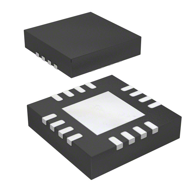
range of -40°C to +125°C and is available in a 16-pin
TQFN thermally enhanced package.
Applications
●● Industrial
●● Home Security/Safety
●● Networking
Features
●● Wide Operating Input Voltage Range (6.5V to 45V)
●● Thermally Enhanced Package Dissipates
2.6W at TA = +70°C (16-Pin TQFN)
●● Guaranteed 400mA Output Current
●● 70μA Quiescent Supply Current
●● Preset 3.3V, 5.0V, or Adjustable 2.5V to 11V Output
Voltage
●● Remote Load Sense Capability
●● Enable Input
●● Integrated μP Reset Circuit with Programmable
Timeout Period
●● Thermal and Short-Circuit Protection
●● -40°C to +125°C Operating Temperature Range
Ordering Information
PART
OUTPUT
VOLTAGE (V)
PIN-PACKAGE
MAX5087AATE+
16 TQFN-EP*
3.3
MAX5087BATE+
16 TQFN-EP*
5.0
MAX5087BATE/V+
16 TQFN-EP*
5.0
Note: All devices are specified over the -40°C to +125°C operating temperature range.
*EP = Exposed paddle.
+Denotes lead-free package.
Pin Configuration
N.C.
13
N.C.
14
N.C.
N.C.
N.C.
CT
RESET
SET
TOP VIEW
12
11
10
9
8
GND
7
OUTSENSE
15
6
OUT
16
5
OUT
1
2
3
4
EN
IN
IN
+
N.C.
MAX5087
TQFN
19-3964; Rev 6; 5/14
�MAX5087
45V, 400mA, Low-Quiescent-Current
Linear Regulator with Adjustable Reset Delay
Absolute Maximum Ratings
IN to GND (do not exceed package power
dissipation)..........................................................-0.3V to +50V
IN to GND (T ≤ 300ms, IOUT ≤ 250mA)..................-0.3V to +42V
EN to GND..............................................................-0.3V to +50V
RESET, OUT, OUTSENSE to GND.........................-0.3V to +12V
IN to OUT................................................................-0.3V to +50V
CT, SET TO GND....................................................-0.3V to +35V
Short-Circuit Duration (VIN ≤ 14V)..............................Continuous
Maximum Current into Any Pin (Except IN, OUT).............±20mA
Continuous Power Dissipation (TA = +70°C)
16-Pin TQFN (derate 33.3mW/°C above +70°C).......2666mW
Operating Temperature Range...........................-40°C to +125°C
Junction Temperature.......................................................+150°C
Storage Temperature Range..............................-60°C to +150°C
Lead Temperature (soldering, 10s)...................................+300°C
Stresses beyond those listed under “Absolute Maximum Ratings” may cause permanent damage to the device. These are stress ratings only, and functional operation of the device at these
or any other conditions beyond those indicated in the operational sections of the specifications is not implied. Exposure to absolute maximum rating conditions for extended periods may affect
device reliability.
Package Thermal Characteristics (Note 1)
TQFN
Junction-to-Ambient Thermal Resistance (θJA)........30.0°C/W
Junction-to-Case Thermal Resistance (θJC)..................2°C/W
Note 1: Package thermal resistances were obtained using the method described in JEDEC specification JESD51-7, using a four-layer
board. For detailed information on package thermal considerations, refer to www.maximintegrated.com/thermal-tutorial.
Electrical Characteristics
(VIN = 14V, IOUT = 1mA, CIN = 47μF (low ESR), COUT = 15μF, VEN = 2.4V, 10kΩ from RESET to OUT, TA = TJ = -40°C to +125°C,
unless otherwise noted. Typical specifications are at TA = +25°C.) (Note 2)
PARAMETER
Input Voltage Range
Supply Current
Shutdown Supply Current
SYMBOL
CONDITIONS
VIN
VIN ≥ VOUT + 1.5V
IQ
Measured at GND, IOUT = 0
SET = GND
IOUT = 400mA
ISHDN
MIN
TYP
6.5
70
MAX
UNITS
45.0
V
150
5300
VEN P 0.4V
11
21
µA
µA
REGULATOR
Guaranteed Output Current
IOUT
VIN = 6.5V, VOUT = 5.0V
SET = GND,
5V version
Output Voltage (Note 3)
VOUT
SET = GND,
3.3V version
ΔVDO
Startup Response Time
Line Regulation
ΔVOUT /
ΔVIN
Enable Voltage
VEN
www.maximintegrated.com
mA
6.5V P VIN ≤ 25V,
5mA P IOUT ≤ 400mA
4.87
5
5.13
6.5V P VIN ≤ 45V,
5mA P IOUT ≤ 100mA
4.850
5
5.150
6.5V P VIN ≤ 25V,
5mA P IOUT ≤ 400mA
3.208
3.3
3.392
6.5V P VIN ≤ 45V,
5mA P IOUT ≤ 100mA
3.208
3.3
3.392
IOUT = 5mA, adjustable range
Dropout Voltage
400
2.5
11.0
IOUT = 400mA, VOUT = 5V (Note 4)
0.9
Rising edge of VIN to VOUT,
RL = 500Ω, SET = GND (Note 5)
400
8V ≤ VIN ≤ 45V
5V version
3.3V version
VEN = high, regulator on
VEN = low, regulator off
V
2.2
V
µs
-1
+1
-0.5
+0.5
2.4
0.4
mV/V
V
Maxim Integrated │ 2
�MAX5087
45V, 400mA, Low-Quiescent-Current
Linear Regulator with Adjustable Reset Delay
Electrical Characteristics (continued)
(VIN = 14V, IOUT = 1mA, CIN = 47μF (low ESR), COUT = 15μF, VEN = 2.4V, 10kΩ from RESET to OUT, TA = TJ = -40°C to +125°C,
unless otherwise noted. Typical specifications are at TA = +25°C.) (Note 2)
PARAMETER
Enable Input Current
SYMBOL
IEN
CONDITIONS
MIN
TYP
VEN = 2.4V
0.35
VEN = 14V
3.4
MAX
UNITS
µA
SET Reference Voltage
VSET
1.200
1.235
1.260
V
SET Input Leakage Current
ISET
-100
+0.5
+100
nA
IOUT = 1mA to 400mA (Note 3)
0.1
0.35
Ω
IOUT = 10mA, f = 100Hz, 500mVP-P,
VOUT = 5V
70
dB
VIN < 14V (Note 6)
640
mA
175
°C
Load Regulation
Power-Supply Rejection Ratio
Short-Circuit Current
Thermal Shutdown Temperature
Thermal Shutdown Hysteresis
ΔVOUT /
ΔIOUT
PSRR
ISC
TJ(SHDN)
ΔTJ(SHDN)
RESET Voltage Threshold
VRESET
RESET Threshold Hysteresis
VRHYST
25
89
92
°C
94
2
% VOUT
% VOUT
RESET Output Low Voltage
VRL
ISINK = 1mA
0.4
V
RESET Output Leakage Current
IRH
VRESET = 5V
1
µA
RESET Output Minimum Timeout
Period
When VOUT reaches RESET threshold,
CCT = Open
15
µs
ENABLE to RESET Minimum
Timeout Period
When EN goes high, CCT = open
170
µs
Delay Comparator Threshold
(Rising)
1.196
Delay Comparator Threshold
Hysteresis
CT Charge Current
CT Discharge Current
Note
Note
Note
Note
Note
2:
3:
4:
5:
6:
1.230
1.264
100
1
2
V
mV
4
5
µA
mA
Limits at TA = -40°C are guaranteed by design.
Output voltage is tested using a pulsed load current of less than 50ms duration.
Dropout voltage is defined as (VIN - VOUT) when VOUT is 100mV below the value of VOUT for VIN = VOUT + 3V.
Startup time measured from 50% of VIN to 90% of VOUT.
Continuous short-circuit protection for VIN > 14V not guaranteed.
www.maximintegrated.com
Maxim Integrated │ 3
�MAX5087
45V, 400mA, Low-Quiescent-Current
Linear Regulator with Adjustable Reset Delay
Typical Operating Characteristics
(VIN = VEN = 14V, CIN = 47μF (low ESR), COUT = 15μF, VOUT = 5V, SET = GND, TA = +25°C, unless otherwise specified.)
4.5
IGND (A)
3.0
2.5
2.0
1.5
1.0
IOUT = 0
0.5
15
20
25
30
35
40
45
-40 -25 -10 5 20 35 50 65 80 95 110 125
6
VIN = +6.5V
5
5.05
5.00
4.95
IOUT = 400mA
3
2
4.85
IOUT = 50mA
IOUT = 5mA
0
-40 -25 -10 5 20 35 50 65 80 95 110 125 140
VIN = +6.5V
5.15
IOUT = 100mA
5.05
IOUT = 50mA
5.00
4.95
IOUT = 400mA
4.85
4.80
-40 -25 -10 5 20 35 50 65 80 95 110 125 140
4.75
-40 -25 -10 5 20 35 50 65 80 95 110 125 140
TEMPERATURE (°C)
TEMPERATURE (°C)
TEMPERATURE (°C)
DROPOUT VOLTAGE
vs. LOAD CURRENT
POWER-SUPPLY REJECTION RATIO
vs. FREQUENCY
LOAD-TRANSIENT RESPONSE
0
MAX5087 toc07
1.35
1.20
0.75
0.60
0.45
0.30
0.15
VOUT = +5V
100 150 200 250 300 350 400
IOUT (mA)
www.maximintegrated.com
MAX5087 toc09
IOUT = 5mA
VOUT
200mV/div
AC-COUPLED
-20
PSRR (dB)
0.90
COUT = 15F
IOUT = 10mA
-10
1.05
50
5.20
4.90
IOUT = 100mA
1
4.80
5.25
5.10
4
0
-40 -25 -10 5 20 35 50 65 80 95 110 125 140
OUTPUT VOLTAGE
vs. LOAD CURRENT AND TEMPERATURE
IGND (mA)
VOUT (V)
2
0
GROUND CURRENT
vs. TEMPERATURE (PULSED LOAD)
4.90
VDROPOUT (V)
4
OUTPUT VOLTAGE
vs. TEMPERATURE
5.10
0
6
TEMPERATURE (°C)
5.15
1.50
8
TEMPERATURE (°C)
5.20
4.75
10
VIN (V)
MAX5087 toc04
5.25
10
VIN = +6.5V
12
MAX5087 toc06
5
16
MAX5087 toc05
0
VIN = +14V
50
40
30
20
10
0
18
VOUT (V)
0
SHUTDOWN SUPPLY CURRENT
vs. TEMPERATURE
14
80
70
60
MAX5087 toc08
VOUT (V)
4.0
3.5
VIN = +45V
100
90
20
ISHDN (A)
5.0
MAX5087 toc02
120
110
MAX5087 toc01
5.5
NO-LOAD SUPPLY CURRENT
vs. TEMPERATURE
MAX5087 toc03
OUTPUT VOLTAGE vs.
INPUT VOLTAGE
-30
-40
-50
400mA
-60
IOUT
200mA/div
-70
5mA
-80
0.1
1
10
100
1000
400s/div
FREQUENCY (kHz)
Maxim Integrated │ 4
�MAX5087
45V, 400mA, Low-Quiescent-Current
Linear Regulator with Adjustable Reset Delay
Typical Operating Characteristics (continued)
(VIN = VEN = 14V, CIN = 47μF (low ESR), COUT = 15μF, VOUT = 5V, SET = GND, TA = +25°C, unless otherwise specified.)
INPUT VOLTAGE STEP RESPONSE
STARTUP RESPONSE
MAX5087 toc10
IOUT = 50mA
ENABLE STARTUP RESPONSE
MAX5087 toc11
MAX5087 toc12
IOUT = 5mA
VOUT
AC-COUPLED
500mV/div
EN
1V/div
VOUT
2V/div
0V
0V
0V
400s/div
VOUT
2V/div
VIN
10V/div
400s/div
100s/div
ENABLE STARTUP RESPONSE
ENABLE STARTUP RESPONSE
ENABLE STARTUP RESPONSE
MAX5087 toc14
MAX5087 toc13
EN
1V/div
MAX5087 toc15
EN
1V/div
0V
EN
1V/div
0V
0V
VOUT
2V/div
VOUT
2V/div
VIN = 14V
IOUT = 400mA
0V
VIN = 14V
IOUT = 0
0V
VOUT
2V/div
VIN = 45V
IOUT = 0
0V
VIN = 45V
IOUT = 400mA
0V
100s/div
100s/div
100s/div
SHUTDOWN RESPONSE
GROUND CURRENT DISTRIBUTION
(TA = -40°C)
GROUND CURRENT DISTRIBUTION
(TA = +125°C)
40
0V
VOUT
2V/div
20ms/div
30
25
20
15
30
25
20
15
10
5
5
0
51 52 53 54 55 56 57 58 59 60 61 62 63 64 65
150 UNITS
TESTED
35
10
IGND (A)
www.maximintegrated.com
40
NUMBER OF UNITS
EN
1V/div
150 UNITS
TESTED
35
NUMBER OF UNITS
0V
MAX5087 toc17
MAX5087 toc16
IOUT = 5mA
MAX5087 toc18
26V
VIN
10V/div
6.5V
0
63 65 66 67 68 69 70 71 72 73 74 75 76
IGND (A)
Maxim Integrated │ 5
�MAX5087
45V, 400mA, Low-Quiescent-Current
Linear Regulator with Adjustable Reset Delay
Pin Description
PIN
NAME
1, 12–16
N.C.
2
EN
Enable Input. Drive EN high to turn on the regulator. Force EN low to place the device in shutdown mode.
3, 4
IN
Regulator Input. Supply voltage ranges from 6.5V to 45V. Bypass IN to GND with a low-ESR 47µF
electrolytic capacitor.
5, 6
OUT
7
OUTSENSE
8
GND
Ground
9
SET
Feedback Regulation Set Point. Connect SET to GND for a fixed 3.3V output (MAX5087A) or 5.0V
output (MAX5087B). Connect an external resistive divider network from OUTSENSE to SET to GND to
adjust the output voltage from 2.5V to 11V.
10
RESET
11
CT
Reset Timeout Setting Connection. A 2µA charging current is available at CT. Connect a capacitor from
CT to GND to set the reset timeout period (see the Adjustable Reset Timeout Period (CT) section).
—
EP
Exposed Paddle. Connect externally to a large ground plane to aid heat dissipation. Do not use EP as a
ground connection.
www.maximintegrated.com
FUNCTION
No Connection. Not internally connected.
Regulator Output. Connect at least a 15µF low-ESR capacitor from OUT to GND.
Regulator Output Feedback Point. OUTSENSE must be connected to OUT for fixed output voltage
versions. Leave OUTSENSE open for adjustable output voltage version.
Open-Drain Active-Low Reset Output. Connect a 10kΩ pullup resistor from RESET to any supply
voltage up to 11V to create a logic output.
Maxim Integrated │ 6
�MAX5087
45V, 400mA, Low-Quiescent-Current
Linear Regulator with Adjustable Reset Delay
IN
ERROR
AMPLIFIER
MAX5087
VREF
1.235V
CONTROL LOGIC,
THERMAL SHUTDOWN,
AND
OVERCURRENT
PROTECTION
OUTSENSE
MUX
EN
OUT
INTERNAL
SUPPLY VOLTAGE
SET
2µA
CT
DELAY
COMPARATOR
CT
COMPARATOR
RESET
0.92 x VREF
GND
Figure 1. Functional Diagram
www.maximintegrated.com
Maxim Integrated │ 7
�MAX5087
45V, 400mA, Low-Quiescent-Current
Linear Regulator with Adjustable Reset Delay
Detailed Description
The MAX5087 high-voltage linear regulator includes
an integrated μP reset circuit with an adjustable reset
timeout period (see the Adjustable Reset Timeout Period
(CT) section). The device guarantees a 400mA load current and is available with a preset output voltage of 3.3V
(MAX5087A) or 5V (MAX5087B). Both devices can be
configured to provide an adjustable output voltage from
2.5V to 11V. The internal reset circuit monitors the regulator output voltage and asserts RESET low when the regulator output falls below the reset threshold voltage. Other
features include an enable (regulator control input), 21μA
(max) shutdown current, short-circuit protection (see the
Output Short-Circuit Current Limit section), and thermal
shutdown (see the Thermal Protection section).
Regulator
The MAX5087 accepts an input voltage range from 6.5V
to 45V and offers a fixed output voltage of 3.3V or 5V. For
an adjustable output voltage operation, use an external
resistive divider network connected between OUT, SET,
and GND (see Figure 2).
Enable Input (EN)
EN is a logic-level enable input that turns the device on/
off. Drive EN high to turn on the device and drive EN low
to place the device in shutdown. The MAX5087 draws
11μA (typ) of supply current when in shutdown. EN withstands voltages up to +45V, allowing EN to be connected
to IN for an always-on operation.
Remote Sensing (OUTSENSE)
The 3.3V (MAX5087A) and 5V (MAX5087B) output
voltage versions connect OUTSENSE for load voltage
sensing. Leave OUTSENSE open when using adjustable
output voltage version.
Reset Output (RESET)
A supervisor circuit is fully integrated in the MAX5087 and
uses the same reference voltage as the regulator. RESET
goes low if VOUT drops below the preset output voltage
threshold, and remains low at least for the timeout period
after VOUT rises above the reset voltage threshold.
www.maximintegrated.com
6.5V TO 45V
47µF
2.5V TO 11V
OUT
IN
15µF
MAX5087
R1
ON
EN
OFF
TO µP
CCT
OUTSENSE
RESET
CT
GND
SET
R2
VOUT = VSET (1 + R1 / R2)
VSET = 1.235V
Figure 2. Setting the Adjustable Output Voltage
Adjustable Reset Timeout Period (CT)
The MAX5087 features a user-adjustable reset timeout.
Connect a capacitor from CT to GND to set the reset timeout period (see Figure 2) and use the following equation
to calculate the timeout period:
tRP = CCT x 0.6175 x 10⁶ (s)
where CCT is the value of the external capacitor connected from CT to GND.
Thermal Protection
When the junction temperature exceeds TJ = +175°C, an
internal thermal sensor signals the shutdown logic, which
turns off the pass transistor, allowing the IC to cool. The
thermal sensor turns the pass transistor on again after
the IC’s junction temperature cools by 25°C, resulting in
a cycled output during continuous thermaloverload conditions. Thermal protection protects the MAX5087 in the
event of fault conditions. During continuous operation, do
not exceed the absolute maximum junction temperature
rating of TJ = +150°C.
Output Short-Circuit Current Limit
The MAX5087 features a current limit. The output can be
shorted to GND for an indefinite period of time (for VIN <
14V) without damage to the device. Continuous output
short-circuit protection is only guaranteed for VIN < 14V.
Maxim Integrated │ 8
�MAX5087
45V, 400mA, Low-Quiescent-Current
Linear Regulator with Adjustable Reset Delay
Applications Information
VOUT
=
3.5
3.0
2.5
PD (W)
The MAX5087 features a Dual ModeTM operation, in
either a preset-voltage mode or an adjustable mode. In
preset-voltage mode, internal feedback resistors set the
MAX5087’s output voltage to +3.3V or +5V. Select presetvoltage mode by connecting SET to ground. In adjustable
mode, select an output between +2.5V and +11V using
two external resistors connected as a voltage-divider to
SET (Figure 2). Set the output voltage using the following
equation:
Available Output-Current Calculation
The MAX5087 high-voltage regulator provides up to
400mA of output current. The input voltage extends to
+45V. Package power dissipation limits the amount of output current available for a given input/output voltage and
ambient temperature. Figure 3 shows the maximum power
dissipation curve for these devices. The graph assumes
that the exposed paddle of the MAX5087 package is set
up per JEDEC 51 (multilayer board) specifications.
Use Figure 3 to determine the allowable package dissipation (PD) for a given ambient temperature. Alternately,
use the following formulas to calculate the allowable
package dissipation. Note that for the examples shown
below, the electrical characteristic limits are guaranteed
up to TJ = +125°C (max).
2.666W for TA ≤ + 70°C
W
PD 2.666W − 0.0333 × (TA − 70°C)
=
C
°
for + 70°C < TA ≤ + 125°C
After determining the allowable package dissipation calculate the maximum output current using the following
formula:
PD
I OUT(MAX) ≅
≤ 400mA
VIN − VOUT
2.666W
(16-PIN TQFN)
2.0
1.5
DERATE
33.3mW/°C
1.0
0.5
0
R1
VSET × 1 +
R2
where VSET = 1.235V and R2 is chosen to be < 100kΩ.
MAX5087 fig03
4.0
Output-Voltage Selection
0
20
40
60
80
100 120 140
TEMPERATURE (°C)
Figure 3. Calculated Maximum Power Dissipation vs.
Temperature
The above equations do not include the negligible power
dissipation from self-heating due to the IC ground current.
Example 1:
TA = +95°C
VIN = +14V
VOUT = +5V
Find the maximum allowable output current. First calculate package dissipation at the given temperature as
follows:
=
PD 2.666W − 0.0333
W
(95°C − 70
=
°C) 1.8335W
°C
Then determine the maximum output current:
=
I OUT(MAX)
(1.8335W)
= 203mA
(14V) − (5V)
Example 2:
TA = +125°C
VIN = +14V
VOUT = +5V
Dual Mode is a trademark of Maxim Integrated Products, Inc.
www.maximintegrated.com
Maxim Integrated │ 9
�45V, 400mA, Low-Quiescent-Current
Linear Regulator with Adjustable Reset Delay
Calculate package dissipation at the given temperature
as follows:
°
(125°C − 70
=
°C) 0.8345W
And establish the maximum current:
(1.191W)
= 92.7mA
(14V) − (5V)
=
I OUT(MAX)
0.40
TA = +70°C
TA = +85°C
TA = +125°C
0.35
0.30
0.25
0.20
0.15
0.10
Example 3:
0.05
TA = +50°C
0
VIN = +14V
VOUT = +5V
0.45
IOUT(MAX) (A)
=
P
2.666W − 0.0333
0.50
MAX5087 fig04
MAX5087
0
5
10
15
20
25
30
35
40
45
VIN (V)
VOUT = +10V
Calculate package dissipation at the given temperature
as follows:
PD = 2.666W
And find the maximum output current:
(2.666W)
I OUT(MAX) =
666mA ⇒ I OUT(MAX) =
400mA
=
(14V) − (10V)
In example 3 the maximum output current is calculated
as 666mA, however, the maximum output current cannot
exceed 400mA.
Use Figure 4 to quickly determine maximum allowable
output current for selected ambient temperatures.
www.maximintegrated.com
Figure 4. Maximum Output Current vs. Input Voltage (16-Pin
TQFN)
Output-Capacitor Selection and
Regulator Stability
For stable operation over the full temperature range and
with load currents up to 400mA, use a 15μF (min) output
capacitor with an ESR < 0.25Ω. To reduce noise and
improve load-transient response, stability, and powersupply rejection use larger output capacitor values such
as 22μF.
Some ceramic capacitor dielectrics exhibit large capacitance and ESR variation with temperature. For capacitor
dielectrics such as Y5V, use 22μF or more to ensure
stability at temperatures below -10°C. With X7R or X5R
dielectrics, 15μF should be sufficient at all operating temperatures. To improve power supply rejection and transient response, use a minimum 47μF low-ESR capacitor
from IN to GND.
Maxim Integrated │ 10
�MAX5087
Chip Information
PROCESS: BiCMOS
www.maximintegrated.com
45V, 400mA, Low-Quiescent-Current
Linear Regulator with Adjustable Reset Delay
Package Information
For the latest package outline information and land patterns
(footprints), go to www.maximintegrated.com/packages. Note
that a “+”, “#”, or “-” in the package code indicates RoHS status
only. Package drawings may show a different suffix character, but
the drawing pertains to the package regardless of RoHS status.
PACKAGE
TYPE
PACKAGE
CODE
OUTLINE
NO.
LAND
PATTERN NO.
16 TQFN-EP
T1655+3
21-0140
90-0073
Maxim Integrated │ 11
�MAX5087
45V, 400mA, Low-Quiescent-Current
Linear Regulator with Adjustable Reset Delay
Revision History
REVISION
NUMBER
REVISION
DATE
PAGES
CHANGED
0
2/06
Initial release
1
4/06
Updated Ordering Information and Electrical Characteristics tables.
2
7/06
Updated Electrical Characteristics table.
3
2/08
Corrected errors in data sheet, reduced operating range, and removed
products from Ordering Information table.
4
4/13
Added /V variant to Ordering Information
1
5
7/13
Changed package code to T1655+3
11
6
5/14
Updated Applications.
1
DESCRIPTION
—
1–3
2
1–13
For pricing, delivery, and ordering information, please contact Maxim Direct at 1-888-629-4642, or visit Maxim Integrated’s website at www.maximintegrated.com.
Maxim Integrated cannot assume responsibility for use of any circuitry other than circuitry entirely embodied in a Maxim Integrated product. No circuit patent licenses
are implied. Maxim Integrated reserves the right to change the circuitry and specifications without notice at any time. The parametric values (min and max limits)
shown in the Electrical Characteristics table are guaranteed. Other parametric values quoted in this data sheet are provided for guidance.
Maxim Integrated and the Maxim Integrated logo are trademarks of Maxim Integrated Products, Inc.
© 2014 Maxim Integrated Products, Inc. │ 12
�