19-2658; Rev 1; 10/04
Low-Cost, Voltage-Output, 16-Bit DACs in µMAX
The MAX5204–MAX5207 serial input, voltage-output 16bit digital-to-analog converters (DACs) provide monotonic
16-bit output over temperature without any adjustments.
The MAX5204/MAX5205 operate from a +5V single
power supply and use an external reference ranging
from +4V to VDD, while the MAX5206/MAX5207 operate
from a +3V or +3.3V single power supply and use an
external reference ranging from +2V to V DD . The
MAX5204–MAX5207 DAC output range is typically from
0 to VDD.
The MAX5204–MAX5207 feature a hardware reset input
(CLR) that when pulled low clears the output to zero
code 0000 hex (MAX5205/MAX5207) or resets the output to midscale code 8000 hex (MAX5204/MAX5206).
The 3-wire serial interface is compatible with
SPI™/QSPI™/MICROWIRE™. All devices have a lowpower shutdown mode that reduces the supply current
consumption to 1µA.
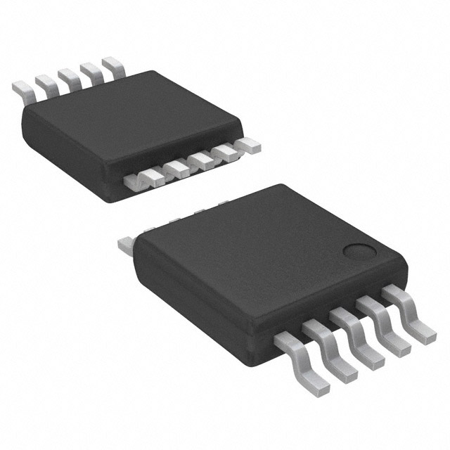
The MAX5204–MAX5207 are available in a space-saving 10-pin µMAX® package and are guaranteed over
the extended temperature range (-40°C to +105°C).
Refer to the MAX5200–MAX5203 data sheet for internal
reference versions.
Applications
Low-Cost VCO/VCXO Frequency Control
Industrial Process Control
High-Resolution Offset Adjustment
Pin Configuration
TOP VIEW
CLR 1
10 DGND
REF
2
AGND
3
VDD
4
7
LDAC
OUT
5
6
CS
MAX5204–
MAX5207
µMAX
9
SCLK
8
DIN
Features
♦ Guaranteed 16-Bit Monotonic
♦ 10-Pin 5mm ✕ 3mm µMAX Package
♦ Rail-to-Rail Output Amplifier
♦ Single-Supply Operation
+5V (MAX5204/MAX5205)
+3V, +3.3V (MAX5206/MAX5207)
♦ Low Power Consumption: 0.5mA
♦ Shutdown Mode Reduces Supply Current to 1µA
♦ SPI/QSPI/MICROWIRE-Compatible 3-Wire Serial
Interface
♦ Power-On-Reset Sets Output to
Midscale (MAX5204/MAX5206)
Zero-Scale (MAX5205/MAX5207)
Ordering Information
PART
TEMP RANGE
PIN-PACKAGE
MAX5204AEUB
-40°C to +105°C
10 µMAX
MAX5204BEUB
-40°C to +105°C
10 µMAX
MAX5204ACUB
0°C to +70°C
10 µMAX
MAX5205AEUB
-40°C to +105°C
10 µMAX
MAX5205BEUB
-40°C to +105°C
10 µMAX
MAX5205ACUB
0°C to +70°C
10 µMAX
MAX5206AEUB
-40°C to +105°C
10 µMAX
MAX5206BEUB
-40°C to +105°C
10 µMAX
MAX5206ACUB
0°C to +70°C
10 µMAX
MAX5207AEUB
-40°C to +105°C
10 µMAX
MAX5207BEUB
-40°C to +105°C
10 µMAX
MAX5207ACUB
0°C to +70°C
10 µMAX
Selector Guide appears at end of data sheet.
SPI/QSPI are trademarks of Motorola, Inc.
MICROWIRE is a trademark of National Semiconductor Corp.
µMAX is a registered trademark of Maxim Integrated Products, Inc.
________________________________________________________________ Maxim Integrated Products
For pricing, delivery, and ordering information, please contact Maxim/Dallas Direct! at
1-888-629-4642, or visit Maxim’s website at www.maxim-ic.com.
1
MAX5204–MAX5207
General Description
�MAX5204–MAX5207
Low-Cost, Voltage-Output, 16-Bit DACs in µMAX
ABSOLUTE MAXIMUM RATINGS
VDD to AGND, DGND ...............................................-0.3V to +6V
AGND to DGND.........................................……….-0.3V to +0.3V
REF, OUT to AGND.................................…-0.3V to (VDD + 0.3V)
CLR, LDAC, SCLK, DIN, CS to DGND .......-0.3V to (VDD + 0.3V)
Maximum Current into Any Pin............................................50mA
Continuous Power Dissipation (TA = +70°C)
10-Pin µMAX (derate 5.6mW/°C above +70°C) .........444.4mW
Operating Temperature Ranges
MAX520_CUB ......................................................0°C to +70°C
MAX520_EUB .........................................…….-40°C to +105°C
Junction Temperature ......................................................+150°C
Storage Temperature Range .............................-60°C to +150°C
Lead Temperature (soldering, 10s) .................................+300°C
Stresses beyond those listed under “Absolute Maximum Ratings” may cause permanent damage to the device. These are stress ratings only, and functional
operation of the device at these or any other conditions beyond those indicated in the operational sections of the specifications is not implied. Exposure to
absolute maximum rating conditions for extended periods may affect device reliability.
ELECTRICAL CHARACTERISTICS—MAX5204/MAX5205
(VDD = +4.75V to +5.25V, fSCLK = 10MHz (50% duty cycle), VREF = 4.096V, output load = 10kΩ in parallel with 250pF, TA = TMIN to
TMAX, unless otherwise noted. Typical values are at TA = +25°C.)
PARAMETER
SYMBOL
CONDITIONS
MIN
TYP
MAX
MAX520_AEUB
±10
±20
MAX520_ACUB
±10
±20
MAX520_BEUB
±20
±40
UNITS
STATIC PERFORMANCE (Note 1)
Resolution
Integral Nonlinearity (Note 2)
Differential Nonlinearity
(Note 2)
N
INL
DNL
GE
Bits
MAX520_A_UB (Note 3)
±1
MAX520_BEUB (0°C to +105°C) (Note 3)
±1
MAX520_BEUB (-40°C to 0°C)
±2
Inferred from measurement at 1C00 hex
and FFFF hex
Offset Error
Gain Error
16
Within DAC output range (Note 4)
LSB
LSB
±3
±25
mV
±0.01
±1
%FSR
Offset Temperature Coefficient
1.5
µV/°C
Gain Temperature Coefficient
3
ppm of
FSR/°C
Power-Supply Rejection
PSR
VDD = 5V ±5%, midscale input
±0.06
±0.5
mV/V
DYNAMIC PERFORMANCE
DAC Output Range
Output-Voltage Slew Rate
(Note 2)
V
0.6
V/µs
To ±1LSB of FS,
VSTEP = 0.25 × VREF to 0.75 × VREF
25
µs
Output Noise
DAC code = 8400 hex, 10kHz
120
nV/√Hz
DAC Glitch Impulse
Major carry transition (code 7FFF hex to
code 8000 hex)
10
nV⋅s
Digital Feedthrough
Code = 0000 hex; CS = VDD;
LDAC = 0; SCLK, DIN = 0 or VDD
10
nV⋅s
Wake-Up Time
From software shutdown to 90% of output
code = FFFF hex
50
µs
Power-Up Time
From power applied to 90% of output
code = FFFF hex
10
ms
Output Settling Time
2
SR
0 to
VDD
_______________________________________________________________________________________
�Low-Cost, Voltage-Output, 16-Bit DACs in µMAX
(VDD = +4.75V to +5.25V, fSCLK = 10MHz (50% duty cycle), VREF = 4.096V, output load = 10kΩ in parallel with 250pF, TA = TMIN to
TMAX, unless otherwise noted. Typical values are at TA = +25°C.)
PARAMETER
SYMBOL
CONDITIONS
MIN
TYP
MAX
UNITS
REFERENCE INPUT
VREF Input Range
4.0
VDD
V
VREF Input Current
40
µA
VREF Input Resistance
100
kΩ
Input Capacitance
18
pF
DIGITAL INPUTS (DIN, SCLK, CS, CLR, LDAC)
Input High Voltage
VIH
Input Low Voltage
VIL
Input Hysteresis
2.4
VHYST
Input Leakage
IIN
Input Capacitance
CIN
V
0.8
200
Digital inputs = 0 or VDD
V
mV
±1
15
µA
pF
POWER REQUIREMENTS
Positive Power Supply
VDD
Positive Supply Current
IDD
Shutdown Supply Current
ISHDN
4.75
All digital inputs at 0 or VDD (Note 5)
All digital inputs at 0 or VDD
5.25
V
0.8
1.5
mA
1
10
µA
10
MHz
TIMING CHARACTERISTICS
SCLK Frequency
fSCLK
SCLK Clock Period
tCP
100
ns
SCLK Pulse Width High
tCH
40
ns
SCLK Pulse Width Low
tCL
40
ns
DIN Setup Time
tDS
40
ns
ns
DIN Hold Time
tDH
0
CS Fall to SCLK Rise Setup Time
tCSS
40
ns
SCLK Rise to CS Rise Hold Time
tCSH
0
ns
SCLK Rise to CS Fall Ignore
tCS0
10
ns
CS Rise to SCLK Rise Ignore
tCS1
40
ns
LDAC Pulse Width
tLDAC
40
ns
CS Rise to LDAC Low Setup
tLDACS
40
ns
SCLK Fall to CS Fall Ignore
tCSOL
10
ns
CS Pulse Width Low for Shutdown
tCSWL
40
ns
CS Pulse Width High
tCSWH
100
ns
_______________________________________________________________________________________
3
MAX5204–MAX5207
ELECTRICAL CHARACTERISTICS—MAX5204/MAX5205 (continued)
�MAX5204–MAX5207
Low-Cost, Voltage-Output, 16-Bit DACs in µMAX
ELECTRICAL CHARACTERISTICS—MAX5206/MAX5207
(VDD = +2.7V to +3.6V, fSCLK = 10MHz (50% duty cycle), VREF = 2.048V, output load = 10kΩ in parallel with 250pF, TA = TMIN to TMAX,
unless otherwise noted. Typical values are at TA = +25°C.)
PARAMETER
SYMBOL
CONDITIONS
MIN
TYP
MAX
UNITS
STATIC PERFORMANCE (Note 1)
Resolution
Integral Nonlinearity (Note 2)
Differential Nonlinearity (Note 2)
N
INL
DNL
GE
Bits
MAX520_AEUB
±10
±20
MAX520_ACUB
±10
±20
MAX520_BEUB
±20
±40
MAX520_A_UB (Note 3)
±1
MAX520_BEUB (0°C to +105°C) (Note 3)
±1
MAX520_BEUB (-40°C to 0°C)
±2
Inferred from measurement at 3800 hex and
FFFF hex
Offset Error
Gain Error
16
Within DAC output range (Note 4)
LSB
LSB
±3
±25
mV
±0.01
±1.0
%FSR
Offset Temperature Coefficient
1.5
µV/°C
Gain Temperature Coefficient
3
ppm of
FSR/°C
Power-Supply Rejection
PSR
VDD = 3V ±10%, midscale input
±0.06
±0.5
mV/V
DYNAMIC PERFORMANCE
DAC Output Range
Voltage-Output Slew Rate
(Note 2)
SR
0 to
VDD
V
0.6
V/µs
Output Settling Time
To ±1LSB of FS,
VSTEP = 0.25 ✕ VREF to 0.75 ✕ VREF
25
µs
Output Noise
Code = 8400 hex, 10kHz
120
nV/√Hz
DAC Glitch Impulse
Major carry transition (code 7FFF hex to
code 8000 hex)
10
nV⋅s
Digital Feedthrough
Code = 0000 hex; CS = VDD;
LDAC = 0; SCLK, DIN = 0 or VDD
10
nV⋅s
Wake-Up Time
From software shutdown to 90% of output
code = FFFF hex
50
µs
Power-Up Time
From power boosting to 90% of output
code = FFFF hex
10
ms
REFERENCE INPUT
VREF Input Range
2.0
VDD
V
VREF Input Current
20
µA
VREF Input Resistance
100
kΩ
Input Capacitance
18
pF
4
_______________________________________________________________________________________
�Low-Cost, Voltage-Output, 16-Bit DACs in µMAX
(VDD = +2.7V to +3.6V, fSCLK = 10MHz (50% duty cycle), VREF = 2.048V, output load = 10kΩ in parallel with 250pF, TA = TMIN to TMAX,
unless otherwise noted. Typical values are at TA = +25°C.)
PARAMETER
SYMBOL
CONDITIONS
MIN
TYP
MAX
UNITS
DIGITAL INPUTS (DIN, SCLK, CS, CLR, LDAC)
Input High Voltage
VIH
Input Low Voltage
VIL
Input Hysteresis
2.1
VHYST
Input Leakage
IIN
Input Capacitance
CIN
V
0.6
200
Digital inputs = 0 or VDD
V
mV
±1
15
µA
pF
POWER REQUIREMENTS
Positive Power Supply
VDD
Positive Supply Current
IDD
Shutdown Supply Current
ISHDN
2.7
All digital inputs at 0 or VDD (Note 5)
All digital inputs at 0 or VDD
3.6
V
0.5
1.5
mA
1
10
µA
10
MHz
TIMING CHARACTERISTICS
SCLK Frequency
fSCLK
SCLK Clock Period
tCP
100
ns
SCLK Pulse Width High
tCH
40
ns
SCLK Pulse Width Low
tCL
40
ns
DIN Setup Time
tDS
40
ns
DIN Hold Time
tDH
0
ns
CS Fall to SCLK Rise Setup Time
tCSS
40
ns
SCLK Rise to CS Rise Hold Time
tCSH
0
ns
SCLK Rise to CS Fall Ignore
tCS0
10
ns
CS Rise to SCLK Rise Ignore
tCS1
40
ns
LDAC Pulse Width
tLDAC
40
ns
CS Rise to LDAC Low Setup
tLDACS
40
ns
SCLK Fall to CS Fall Ignore
tCSOL
10
ns
CS Pulse Width Low for Shutdown
tCSWL
40
ns
CS Pulse Width High
tCSWH
100
ns
Note 1:
Note 2:
Note 3:
Note 4:
Note 5:
Static performance tested at VDD = +5.0V (MAX5204/MAX5205) and at VDD = +3.0V (MAX5206/MAX5207).
INL and DNL are guaranteed for outputs between 0.5V to (VDD - 0.5V).
Guaranteed monotonic.
VREF = 4.096V (MAX5204/MAX5205) and VREF = 2.048V (MAX5206/MAX5207).
RL = ∞, digital inputs are at VDD or DGND.
_______________________________________________________________________________________
5
MAX5204–MAX5207
ELECTRICAL CHARACTERISTICS—MAX5206/MAX5207 (continued)
�Typical Operating Characteristics
(VDD = +5V, VREF = 4.096V, TA = +25°C, unless otherwise noted.)
0.6
0.5
0.75
8
0.50
4
0.25
DNL (LSB)
0.7
0
0
25
50
0
-4
-0.25
-8
-0.50
-12
-0.75
-16
-40 -25
75 85
-1.00
0
10000 20000 30000 40000 50000 60000 70000
TEMPERATURE (°C)
0
DAC CODE
OFFSET ERROR
vs. TEMPERATURE
GAIN ERROR
vs. TEMPERATURE
0.30
OFFSET ERROR (mV)
0.06
0.04
0.02
0
-0.02
-0.04
MAX5204 toc06
MAX5204 toc05
0.08
10000 20000 30000 40000 50000 60000 70000
DAC CODE
HALF-SCALE OUTPUT SETTLING TIME
(CODE FROM 4000H TO C000H)
0.40
MAX5204 toc04
0.10
MAX5204 toc03
12
INL (LSB)
0.8
1.00
MAX5204 toc02
0.9
SUPPLY CURRENT (mA)
16
MAX5204 toc01
1.0
DIFFERENTIAL NONLINEARITY
vs. CODE
INTEGRAL NONLINEARITY
vs. CODE (A GRADE)
SUPPLY CURRENT vs. TEMPERATURE
GAIN ERROR (%FSR)
0.20
LARGE SIGNAL
(1V/div)
0.10
0
-0.10
SMALL SIGNAL
(1mV/div)
-0.20
-0.06
-0.30
-0.08
-0.10
-20
0
20
40
60
80
-0.40
-40
-20
0
20
40
60
80
4µs/div
TEMPERATURE (°C)
TEMPERATURE (°C)
OUTPUT NOISE DENSITY
vs. FREQUENCY
HALF-SCALE OUTPUT SETTLING TIME
(CODE FROM C000H TO 4000H)
700
MAX5204 toc07
DAC CODE = 8400 HEX
LARGE SIGNAL
(1V/div)
OUT
1V/div
OUT
1mV/div
SMALL SIGNAL
(1mV/div)
RLOAD = 10kΩ
CLOAD = 250pF
600
500
400
300
200
100
0
100
4µs/div
6
MAX5204 toc08
-40
RLOAD = 10kΩ
CLOAD = 250pF
VOLTAGE NOISE DENSITY (nV/√Hz)
MAX5204–MAX5207
Low-Cost, Voltage-Output, 16-Bit DACs in µMAX
1000
10,000
100,000
FREQUENCY (Hz)
_______________________________________________________________________________________
OUT
1V/div
OUT
1mV/div
�Low-Cost, Voltage-Output, 16-Bit DACs in µMAX
CODE = FFFF HEX
CODE = C000 HEX
2.5
2.0
CODE = 8000 HEX
1.5
4.0
3.5
OUTPUT VOLTAGE (V)
3.0
2.5
2.0
OUT
(AC-COUPLED,
5mV/div)
CODE = 4000 HEX
1.5
1.0
1.0
0.5
0.5
CODE = 0000 HEX
0
0
10
20
30
40
0
3
6
9
15
12
1µs/div
SINK CURRENT (mA)
SOURCE CURRENT (mA)
SHUTDOWN CURRENT
vs. TEMPERATURE
MAJOR-CARRY OUTPUT GLITCH
(CODE FROM 7FFFH TO 8000H)
MAX5204 toc12
1.00
MAX5204 toc13
0
0.75
OUT
(AC-COUPLED,
5mV/div)
SHUTDOWN CURRENT (µA)
OUTPUT VOLTAGE (V)
3.5
MAX5204 toc11
MAX5204 toc10
4.0
3.0
4.5
MAX5204 toc09
4.5
MAJOR-CARRY OUTPUT GLITCH
(CODE FROM 8000H TO 7FFFH)
SINK-CURRENT CAPABILITY
SOURCE-CURRENT CAPABILITY
0.50
0.25
0
-0.25
-0.50
-0.75
-1.00
1µs/div
-40
-20
0
20
40
60
80
TEMPERATURE (°C)
_______________________________________________________________________________________
7
MAX5204–MAX5207
Typical Operating Characteristics (continued)
(VDD = +5V, VREF = 4.096V, TA = +25°C, unless otherwise noted.)
�Low-Cost, Voltage-Output, 16-Bit DACs in µMAX
MAX5204–MAX5207
Pin Description
PIN
NAME
1
CLR
2
REF
3
AGND
FUNCTION
Reset DAC Active-Low Input. Pull CLR low to reset the DAC output to midscale output (8000 hex) for
MAX5204/MAX5206 and to zero-scale output (0000 hex) for MAX5205/MAX5207. For normal operation,
connect CLR to VDD.
External Reference Voltage Input
Analog Ground
4
VDD
5
OUT
Positive Supply Voltage. Bypass VDD to AGND with a 10µF capacitor in parallel with a 0.1µF capacitor.
6
CS
7
LDAC
Load DAC Input
8
DIN
Serial Data Input
9
SCLK
Serial Clock Input. Duty cycle must be 40% to 60%.
10
DGND
Digital Ground
DAC Output Voltage
Active-Low Chip-Select Input
Detailed Description
The MAX5204–MAX5207 serial 16-bit, voltage-output
DACs are easily configured with a 3-wire serial interface.
These devices offer full 16-bit performance with less than
±20LSB integral linearity error and less than ±1LSB differential linearity error, thus ensuring monotonic performance. Serial data transfer minimizes the number of
package pins required. The MAX5204–MAX5207 include
control-logic circuitry, a 16-bit data-in shift register, and
a DAC register. The MAX5204–MAX5207 output is
buffered and the full-scale output voltage is VREF (typ).
The MAX5204–MAX5207 feature a hardware reset input
(CLR) that when pulled low clears the DAC output to
zero code 0000 hex (MAX5205/MAX5207) or resets the
DAC output to midscale code 8000 hex (MAX5204/
MAX5206). For normal operation, connect CLR to VDD.
Reference Input
The MAX5204/MAX5205 (+5V supply) use an external
reference between 4V to V DD , while the MAX5206/
MAX5207 (+3V supply) use an external reference from
2V to VDD. The DAC output range is from 0 to VREF.
8
VDD
MAX5204–
MAX5207
REF
BUFFER
16-BIT DAC
OUT
CLR
16-BIT DATA LATCH
CS
SCLK
DIN
LDAC
CONTROL
LOGIC
SERIAL INPUT REGISTER
DGND
AGND
Figure 1. MAX5204–MAX5207 Simplified Functional Diagram
Digital Interface
The MAX5204–MAX5207 digital interface is a standard
3-wire connection compatible with SPI/QSPI/
MICROWIRE and most DSP interfaces. All of the digital
input pins (CS, SCLK, DIN, CLR, and LDAC) are TTL
compatible. SCLK can accept clock frequencies as
high as 10MHz for a +5V supply and 10MHz for a +3V
or +3.3V supply.
One of two methods can be used when interfacing and
updating the MAX5204–MAX5207. The first requires
_______________________________________________________________________________________
�Low-Cost, Voltage-Output, 16-Bit DACs in µMAX
MAX5204–MAX5207
tCP
tCH
SCLK
tCL
tCS1
tCSS
tCSH
tDH
tDS
CS
tCS0
tCSWH
D15
DIN
D14
D0
NOTE: LDAC IS LOGIC LOW.
Figure 2. 3-Wire Interface Timing Diagram
three digital inputs: CS, DIN, and SCLK (Figure 2). The
active-low chip-select input (CS) enables the serial
data loading at the data input (DIN). Pull CS low and
clock in each bit of the 16-bit digital word on the rising
edge of the serial clock (SCLK). Two eight-bit bytes
can be used, and do not require any additional time
between them. Pulling CS high after loading the 16-bit
word transfers that code into the DAC register and then
updates the output. If CS is not kept low during the
entire loading of the 16-bit word, data will be corrupted.
In this case, a new 16-bit word must be loaded. LDAC
must be kept low at all times for the above instructions.
An alternate method of interfacing and updating the
MAX5204–MAX5207 can be done with a fourth digital
input, the active-low load DAC (LDAC). LDAC allows
the output to update asynchronously after CS goes
high. It is useful when updating multiple MAX5204–
MAX5207s synchronously when sharing a single LDAC
and CS line. LDAC must be kept high at all times during the data loading sequence and must only be
asserted when CS is high. Asserting LDAC when CS is
low can cause corrupted data. To operate the
MAX5204–MAX5207 using LDAC, pull LDAC high, pull
CS low, load the 16-bit word as described in the previous paragraph, and pull CS high again. Following these
commands, the DAC output only updates when LDAC
is asserted low (Figure 3).
Shutdown Mode
The low-power shutdown mode reduces supply current
to typically 1µA and a maximum of 10µA. Shutdown
mode is not activated through command words, as is
common among D/A converters. These devices require
careful manipulation of CS and SCLK (Figure 4).
Shutting Down
To shut down the MAX5204–MAX5207, change the
state of SCLK (either a high to low or low to high transition can be used) and pulse two falling CS edges. In
order to keep the device in shutdown mode, SCLK
must not change state. SCLK must remain in the state
it is in after the two CS pulses.
Waking Up
There are two methods to wake up the MAX5204–
MAX5207. Pulse one falling CS edge or transition SCLK.
It takes 50µs typically from the CS falling edge or SCLK
transition for the DAC to return to normal operation.
Power-On Reset
The MAX5204–MAX5207 have a power-on reset circuit
to set the DAC’s output to a known state when VDD is
first applied. The MAX5204/MAX5206 reset to midscale
(code 8000 hex) upon power-up. The MAX5205/
MAX5207 reset to zero-scale (code 0000 hex) upon
power-up. This ensures that unwanted output voltages
do not occur immediately following a system power-up,
such as a loss of power. It is required to apply VDD first
before any other input (DIN, SCLK, CLR, LDAC, CS,
and REF).
_______________________________________________________________________________________
9
�MAX5204–MAX5207
Low-Cost, Voltage-Output, 16-Bit DACs in µMAX
tCP
tCH
SCLK
tCL
tCS1
tCSS
tCSH
tDH
tDS
CS
tCS0
tCSWH
D15
DIN
D14
D0
tLDACS
tLDAC
LDAC
Figure 3. 4-Wire Interface Timing Diagram
tCS0L
SHUTDOWN
WAKE-UP
SCLK
tCSWL
CS
tCSWH
A. WAKING UP USING A THIRD FALLING EDGE ON CS.
SHUTDOWN
tCS0L
WAKE-UP
SCLK
CS
tCSWL
tCSWH
B. WAKING UP USING A TRANSITION ON SCLK.
Figure 4. Shutdown Timing
Applications Information
Power Supply and Bypassing
Considerations
Bypass the power supply with a 10µF capacitor in parallel with a 0.1µF capacitor to AGND. Minimize lead
lengths to reduce lead inductance. If noise becomes
an issue, use shielding and/or ferrite beads to increase
isolation.
10
Output Buffer
The MAX5204–MAX5207 include low-offset, low-noise
buffers enabling the output to source 15mA or sink
5mA. The output buffer operates at a slew rate of
0.6V/µs. With a 1/4 FS to 3/4 FS output transition, the
buffer output typically settles to 1LSB in about 25µs.
The MAX5204–MAX5207 output buffers provide a low
0.2Ω typical output impedance. The MAX5204–
MAX5207 buffer amplifiers typically produce
120nV/√Hz noise at 10kHz.
______________________________________________________________________________________
�Low-Cost, Voltage-Output, 16-Bit DACs in µMAX
MAX5204–MAX5207
VDD
10µF
0.1µF
MC68XXXX
PCS0
MOSI
SCLK
CLR
CS
DIN
SCLK
LDAC
+5V
MAX5204–
MAX5207
DGND
OUT
AGND REF
BIPOLAR OUT
(±VREF)
MAX400
0.1µF
R
R
10µF
Figure 5. MAX5204–MAX5207 Typical Operating Circuit—Bipolar Output
Table 1. Bipolar Code Table
DAC LATCH CONTENTS
MSB
LSB
ANALOG OUTPUT, VOUT
1111 1111 1111 1111
+VREF × (32,767 / 32,768)
1000 0000 0000 0001
+VREF × (1 / 32,768)
1000 0000 0000 0000
0V
0111 1111 1111 1111
-VREF × (1 / 32,768)
0000 0000 0000 0000
-VREF × (32,768 / 32,768)
Bipolar Configuration
The MAX5204–MAX5207 are designed for unipolar operation, but can be used in bipolar applications with an external amplifier and resistors. Figure 5 shows the
MAX5204–MAX5207 configured for bipolar operation. The
op amp is set for unity gain. Table 1 lists the offset binary
code for this circuit. Output voltage range is ±VREF.
Layout Considerations
Digital and AC transient signals coupling to AGND can
create noise at the output. Connect AGND to the highest quality ground available. Use proper grounding
techniques, such as a multilayer board with a lowinductance ground plane. Wire-wrapped boards and
sockets are not recommended. For optimum system
performance, use printed circuit (PC) boards with separate analog and digital ground planes. Connect the
two ground planes together at the low-impedance
power-supply source. Connect DGND and AGND pins
together at the IC. The best ground connection is
achieved by connecting the DAC’s DGND and AGND
together, and then connecting that point to the system
analog ground plane. If the DAC’s DGND is connected
to the system digital ground, digital noise can get
through the DAC’s analog portion.
Chip Information
TRANSISTOR COUNT: 8764
PROCESS: BiCMOS
______________________________________________________________________________________
11
�MAX5204–MAX5207
Low-Cost, Voltage-Output, 16-Bit DACs in µMAX
Selector Guide
PART
INTEGRAL NONLINEARITY
(LSB MAX)
SUPPLY VOLTAGE
RANGE (V)
REFERENCE INPUT
RANGE (V)
POWER-ON-RESET
VALUE
MAX5204AEUB
20
4.75 to 5.25
4 to VDD
Midscale
MAX5204ACUB
20
4.75 to 5.25
4 to VDD
Midscale
MAX5204BEUB
40
4.75 to 5.25
4 to VDD
Midscale
MAX5205AEUB
20
4.75 to 5.25
4 to VDD
Zero
MAX5205ACUB
20
4.75 to 5.25
4 to VDD
Zero
MAX5205BEUB
40
4.75 to 5.25
4 to VDD
Zero
MAX5206AEUB
20
2.7 to 3.6
2 to VDD
Midscale
MAX5206ACUB
20
2.7 to 3.6
2 to VDD
Midscale
MAX5206BEUB
40
2.7 to 3.6
2 to VDD
Midscale
MAX5207AEUB
20
2.7 to 3.6
2 to VDD
Zero
MAX5207ACUB
20
2.7 to 3.6
2 to VDD
Zero
MAX5207BEUB
40
2.7 to 3.6
2 to VDD
Zero
12
______________________________________________________________________________________
�Low-Cost, Voltage-Output, 16-Bit DACs in µMAX
10LUMAX.EPS
e
4X S
10
10
H
0 0.50±0.1
0.6±0.1
1
1
0.6±0.1
BOTTOM VIEW
TOP VIEW
D2
MILLIMETERS
INCHES
MAX
DIM MIN
0.043
A
0.006
0.002
A1
A2
0.030
0.037
0.120
0.116
D1
0.118
0.114
D2
0.116
0.120
E1
0.118
0.114
E2
0.199
0.187
H
0.0157 0.0275
L
L1
0.037 REF
b
0.007
0.0106
e
0.0197 BSC
c
0.0035 0.0078
0.0196 REF
S
α
0°
6°
MAX
MIN
1.10
0.05
0.15
0.75
0.95
3.05
2.95
3.00
2.89
3.05
2.95
2.89
3.00
4.75
5.05
0.40
0.70
0.940 REF
0.270
0.177
0.500 BSC
0.200
0.090
0.498 REF
0°
6°
E2
GAGE PLANE
A2
c
A
b
A1
α
E1
D1
L
L1
FRONT VIEW
SIDE VIEW
PROPRIETARY INFORMATION
TITLE:
PACKAGE OUTLINE, 10L uMAX/uSOP
APPROVAL
DOCUMENT CONTROL NO.
21-0061
REV.
I
1
1
Maxim cannot assume responsibility for use of any circuitry other than circuitry entirely embodied in a Maxim product. No circuit patent licenses are
implied. Maxim reserves the right to change the circuitry and specifications without notice at any time.
Maxim Integrated Products, 120 San Gabriel Drive, Sunnyvale, CA 94086 408-737-7600 ____________________ 13
© 2004 Maxim Integrated Products
Printed USA
is a registered trademark of Maxim Integrated Products.
MAX5204–MAX5207
Package Information
(The package drawing(s) in this data sheet may not reflect the most current specifications. For the latest package outline information,
go to www.maxim-ic.com/packages.)
�