KIT
ATION
EVALU
LE
B
A
IL
A
AV
19-3619; Rev 1; 3/07
14-Bit, 600Msps, High-Dynamic-Performance
DAC with LVDS Inputs
The MAX5890 advanced 14-bit, 600Msps, digital-toanalog converter (DAC) meets the demanding performance requirements of signal synthesis applications
found in wireless base stations and other communications applications. Operating from 3.3V and 1.8V supplies, the MAX5890 DAC supports update rates of
600Msps using high-speed LVDS inputs while consuming only 297mW of power and offers exceptional
dynamic performance such as 80dBc spurious-free
dynamic range (SFDR) at fOUT = 30MHz.
The MAX5890 utilizes a current-steering architecture that
supports a 2mA to 20mA full-scale output current range,
and produces -2dBm to -22dBm full-scale output signal
levels with a double-terminated 50Ω load. The MAX5890
features an integrated 1.2V bandgap reference and control amplifier to ensure high-accuracy and low-noise performance. A separate reference input (REFIO) allows for
the use of an external reference source for optimum flexibility and improved gain accuracy.
The MAX5890 digital inputs accept LVDS voltage levels, and the flexible clock input can be driven differentially or single-ended, AC- or DC-coupled. The
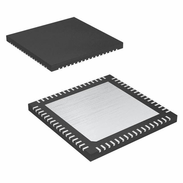
MAX5890 is available in a 68-pin QFN package with an
exposed paddle (EP) and is specified for the extended
(-40°C to +85°C) temperature range.
Refer to the MAX5891 and MAX5889 data sheets for
pin-compatible 16-bit and 12-bit versions of the
MAX5890.
Applications
Features
♦ 600Msps Output Update Rate
♦ Low Noise Spectral Density: -162dBFS/Hz at
fOUT = 36MHz
♦ Excellent SFDR and IMD Performance
SFDR = 80dBc at fOUT = 30MHz (to Nyquist)
SFDR = 68dBc at fOUT = 130MHz (to Nyquist)
IMD = -95dBc at fOUT = 30MHz
IMD = -70dBc at fOUT = 130MHz
♦ ACLR = 73dB at fOUT = 122.88MHz
♦ 2mA to 20mA Full-Scale Output Current
♦ LVDS-Compatible Digital Inputs
♦ On-Chip 1.2V Bandgap Reference
♦ Low 297mW Power Dissipation at 600Msps
♦ Compact (10mm x 10mm) QFN-EP Package
♦ Evaluation Kit Available (MAX5891EVKIT)
Ordering Information
PART
TEMP RANGE
PINPACKAGE
PKG
CODE
MAX5890EGK-D
-40°C to +85°C
68 QFN-EP*
G6800-4
MAX5890EGK+D
-40°C to +85°C
68 QFN-EP*
G6800-4
*EP = Exposed paddle.
D = Dry pack.
+Denotes lead-free package.
Functional Diagram
Base Stations: Single/Multicarrier UMTS,
CDMA, GSM
Communications: Fixed Broadband Wireless
Access, Point-to-Point Microwave
MAX5890
OUTP
Direct Digital Synthesis (DDS)
Cable Modem Termination Systems (CMTS)
Automated Test Equipment (ATE)
D0–D13
LVDS DATA
INPUTS
LVDS
RECEIVER
LATCH
600MHz
14-BIT DAC
OUTN
Instrumentation
DACREF
Selector Guide
PART
RESOLUTION
(BITS)
UPDATE RATE
LOGIC INPUT
(Msps)
MAX5889
12
600
LVDS
MAX5890
14
600
LVDS
MAX5891
16
600
LVDS
1.2V
REFERENCE
CLKP
CLKN
REFIO
FSADJ
CLK
INTERFACE
POWER
DOWN
PD
Pin Configuration appears at end of data sheet.
________________________________________________________________ Maxim Integrated Products
For pricing, delivery, and ordering information, please contact Maxim/Dallas Direct! at
1-888-629-4642, or visit Maxim’s website at www.maxim-ic.com.
1
MAX5890
General Description
�MAX5890
14-Bit, 600Msps, High-Dynamic-Performance
DAC with LVDS Inputs
ABSOLUTE MAXIMUM RATINGS
AVDD1.8, DVDD1.8 to AGND, DGND, DACREF,
and CGND.......................................................-0.3V to +2.16V
AVDD3.3, DVDD3.3, AVCLK to AGND, DGND,
DACREF, and CGND.........................................-0.3V to +3.9V
REFIO, FSADJ to AGND, DACREF,
DGND, and CGND ..........................-0.3V to (AVDD3.3 + 0.3V)
OUTP, OUTN to AGND, DGND, DACREF,
and CGND .......................................-1.2V to (AVDD3.3 + 0.3V)
CLKP, CLKN to AGND, DGND, DACREF,
and CGND..........................................-0.3V to (AVCLK + 0.3V)
PD to AGND, DGND, DACREF,
and CGND.......................................-0.3V to (DVDD3.3 + 0.3V)
Digital Data Inputs (D0N–D13N, D0P–D13P) to AGND,
DGND, DACREF, and CGND ..........-0.3V to (DVDD1.8 + 0.3V)
Continuous Power Dissipation (TA = +70°C) (Note 1)
68-Pin QFN-EP (derate 28.6mW/°C above +70°C)....3333mW
Thermal Resistance θJA (Note 1) ....................................24°C/W
Operating Temperature Range ..........................-40°C to +85°C
Junction Temperature .....................................................+150°C
Storage Temperature Range ............................-60°C to +150°C
Lead Temperature (soldering, 10s) ................................+300°C
Note 1: Thermal resistance based on a multilayer board with 4 x 4 via array in exposed-paddle area.
Stresses beyond those listed under “Absolute Maximum Ratings” may cause permanent damage to the device. These are stress ratings only, and functional
operation of the device at these or any other conditions beyond those indicated in the operational sections of the specifications is not implied. Exposure to
absolute maximum rating conditions for extended periods may affect device reliability.
ELECTRICAL CHARACTERISTICS
(AVDD3.3 = DVDD3.3 = AVCLK = 3.3V, AVDD1.8 = DVDD1.8 = 1.8V, external reference VREFIO = 1.2V, output load 50Ω double-terminated, transformer-coupled output, IOUT = 20mA, TA = -40°C to +85°C, unless otherwise noted. Specifications at TA ≥ +25°C are guaranteed by production testing. Specifications at TA < +25°C are guaranteed by design and characterization. Typical values are at TA
= +25°C.)
PARAMETER
SYMBOL
CONDITIONS
MIN
TYP
MAX
UNITS
STATIC PERFORMANCE
Resolution
14
Bits
Integral Nonlinearity
INL
Measured differentially
±1
LSB
Differential Nonlinearity
DNL
Measured differentially
±0.5
LSB
Offset Error
Full-Scale Gain Error
OS
GEFS
Gain-Drift Tempco
Full-Scale Output Current
External reference
±0.001
+0.02
%FS
-4
±1
+4
%FS
Internal reference
±130
External reference
±100
IOUT
Output Compliance
-0.02
Single-ended
ppm/°C
2
20
mA
-1.0
+1.1
V
Output Resistance
ROUT
1
Output Capacitance
COUT
5
pF
±1
µA
Output Leakage Current
PD = high, power-down mode
MΩ
DYNAMIC PERFORMANCE
Maximum DAC Update Rate
600
Minimum DAC Update Rate
Noise Spectral Density
2
Msps
1
N
fCLK = 500MHz,
-12dBFS, 20MHz
offset from the
carrier
fOUT = 36MHz
AFULL-SCALE = -3.5dBm
-162
fOUT = 151MHz
AFULL-SCALE = -6.4dBm
-153
Msps
dBFS/Hz
_______________________________________________________________________________________
�14-Bit, 600Msps, High-Dynamic-Performance
DAC with LVDS Inputs
(AVDD3.3 = DVDD3.3 = AVCLK = 3.3V, AVDD1.8 = DVDD1.8 = 1.8V, external reference VREFIO = 1.2V, output load 50Ω double-terminated, transformer-coupled output, IOUT = 20mA, TA = -40°C to +85°C, unless otherwise noted. Specifications at TA ≥ +25°C are guaranteed by production testing. Specifications at TA < +25°C are guaranteed by design and characterization. Typical values are at TA
= +25°C.)
PARAMETER
Spurious-Free
Dynamic Range to
Nyquist
SYMBOL
CONDITIONS
fCLK = 200MHz,
0dBFS
fOUT = 30MHz
85
fCLK = 200MHz,
-12dBFS
fOUT = 16MHz
79
fOUT = 30MHz
78
fOUT = 16MHz
80
71
fOUT = 200MHz
55
fCLK = 500MHz
fOUT1 = 29MHz,
fOUT2 = 30MHz,
-6.5dBFS per tone
-95
fCLK = 500MHz
fOUT1 = 129MHz,
fOUT2 = 130MHz,
-6.5dBFS per tone
-70
fCLK = 491.52MHz,
fOUT = 30.72MHz
82
fCLK = 491.52MHz,
fOUT = 122.88MHz
73
fCLK = 491.52MHz,
fOUT = 30.72MHz
74
fCLK = 491.52MHz,
fOUT = 122.88MHz
67
WCDMA single
carrier
ACLR
WCDMA four carriers
BW-1dB
MAX
UNITS
dBc
81
fOUT = 130MHz
TTIMD
Output Bandwidth
76
fOUT = 30MHz
fCLK = 500MHz,
0dBFS
Adjacent Channel
Leakage Power Ratio
TYP
89
SFDR
Two-Tone IMD
MIN
fOUT = 16MHz
dBc
dB
(Note 2)
1000
MHz
REFERENCE
Internal Reference Voltage Range
Reference Input Voltage Range
VREFIO
VREFIOCR
Using external reference
1.14
1.2
1.26
V
0.10
1.2
1.32
V
Reference Input Resistance
RREFIO
10
kΩ
Reference Voltage Temperature
Drift
TCOREF
±50
ppm/°C
ANALOG OUTPUT TIMING (Figure 3)
Output Fall Time
tFALL
90% to 10% (Note 3)
0.4
ns
Output Rise Time
tRISE
10% to 90% (Note 3)
0.4
ns
Reference to data latency (Note 3)
2.5
ns
Output Propagation Delay
tPD
_______________________________________________________________________________________
3
MAX5890
ELECTRICAL CHARACTERISTICS (continued)
�MAX5890
14-Bit, 600Msps, High-Dynamic-Performance
DAC with LVDS Inputs
ELECTRICAL CHARACTERISTICS (continued)
(AVDD3.3 = DVDD3.3 = AVCLK = 3.3V, AVDD1.8 = DVDD1.8 = 1.8V, external reference VREFIO = 1.2V, output load 50Ω double-terminated, transformer-coupled output, IOUT = 20mA, TA = -40°C to +85°C, unless otherwise noted. Specifications at TA ≥ +25°C are guaranteed by production testing. Specifications at TA < +25°C are guaranteed by design and characterization. Typical values are at TA
= +25°C.)
PARAMETER
SYMBOL
CONDITIONS
Output Settling Time
To 0.025% of the final value (Note 3)
Glitch Impulse
Output Noise
NOUT
MIN
TYP
MAX
UNITS
11
ns
Measured differentially
1
pV•s
IOUT = 2mA
30
IOUT = 20mA
30
pA/√Hz
TIMING CHARACTERISTICS
Input Data Rate
600
Data Latency
Clock
cycles
5.5
Data to Clock Setup Time
tSETUP
Referenced to rising edge of clock (Note 4)
-1.5
Data to Clock Hold Time
tHOLD
Referenced to rising edge of clock (Note 4)
2.6
MWps
ns
ns
Clock Frequency
fCLK
CLKP, CLKN
Minimum Clock Pulse-Width High
tCH
CLKP, CLKN
0.6
ns
Minimum Clock Pulse-Width Low
tCL
CLKP, CLKN
0.6
ns
External reference, PD falling edge to
output settle within 1%
350
µs
Turn-On Time
tSHDN
600
MHz
CMOS LOGIC INPUT (PD)
Input Logic-High
VIH
Input Logic-Low
VIL
Input Current
IIN
Input Capacitance
CIN
0.7 x
DVDD3.3
V
0.3 x
DVDD3.3
-10
±1.8
+10
3
V
µA
pF
LVDS INPUTS
Differential Input High
Differential Input Low
VIHLVDS
(Notes 6, 7, 8)
+100
+1000
mV
VILLVDS
(Notes 6, 7, 8)
-1000
-100
mV
1.125
1.375
Internal Common-Mode Bias
VICMLVDS
Differential Input Resistance
RIDLVDS
110
Ω
RICMLVDS
3.2
kΩ
CINLVDS
3
pF
AVCLK / 2
V
0.5
VP-P
1
V
1.9
V
Common-Mode Input Resistance
Input Capacitance
V
DIFFERENTIAL CLOCK INPUTS (CLKP, CLKN)
Clock Common-Mode Voltage
Minimum Differential Input
Voltage Swing
Minimum Common-Mode Voltage
Maximum Common-Mode
Voltage
4
CLKP and CLKN are internally biased
_______________________________________________________________________________________
�14-Bit, 600Msps, High-Dynamic-Performance
DAC with LVDS Inputs
(AVDD3.3 = DVDD3.3 = AVCLK = 3.3V, AVDD1.8 = DVDD1.8 = 1.8V, external reference VREFIO = 1.2V, output load 50Ω double-terminated, transformer-coupled output, IOUT = 20mA, TA = -40°C to +85°C, unless otherwise noted. Specifications at TA ≥ +25°C are guaranteed by production testing. Specifications at TA < +25°C are guaranteed by design and characterization. Typical values are at TA
= +25°C.)
PARAMETER
SYMBOL
Input Resistance
RCLK
Input Capacitance
CCLK
CONDITIONS
MIN
Single-ended
TYP
MAX
UNITS
5
kΩ
3
pF
POWER SUPPLIES
Analog Supply Voltage Range
Clock Supply Voltage Range
Digital Supply Voltage Range
AVDD3.3
3.135
3.3
3.465
AVDD1.8
1.710
1.8
1.890
AVCLK
3.135
3.3
3.465
DVDD3.3
3.135
3.3
3.465
DVDD1.8
1.710
1.8
1.890
IAVDD3.3
Analog Supply Current
IAVDD1.8
Clock Supply Current
IAVCLK
IDVDD3.3
Digital Supply Current
IDVDD1.8
Total Power Dissipation
Power-Supply Rejection Ratio
Note 2:
Note 3:
Note 4:
Note 5:
Note 6:
Note 7:
PDISS
PSRR
fCLK = 100MHz, fOUT = 16MHz
26.5
fCLK = 500MHz, fOUT = 16MHz
26.5
fCLK = 600MHz, fOUT = 16MHz
26.5
fCLK = 100MHz, fOUT = 16MHz
11.3
fCLK = 500MHz, fOUT = 16MHz
50
fCLK = 600MHz, fOUT = 16MHz
60
fCLK = 100MHz, fOUT = 16MHz
2.8
fCLK = 500MHz, fOUT = 16MHz
2.8
fCLK = 600MHz, fOUT = 16MHz
2.8
fCLK = 100MHz, fOUT = 16MHz
0.2
fCLK = 500MHz, fOUT = 16MHz
0.2
V
V
V
28.5
mA
58
3.6
mA
0.5
fCLK = 600MHz, fOUT = 16MHz
0.2
fCLK = 100MHz, fOUT = 16MHz
10.6
fCLK = 500MHz, fOUT = 16MHz
43
fCLK = 600MHz, fOUT = 16MHz
50.5
fCLK = 100MHz, fOUT = 16MHz
137
fCLK = 500MHz, fOUT = 16MHz
264
fCLK = 600MHz, fOUT = 16MHz
297
Power-down, clock static low,
data input static
13
µW
±0.025
%FS
(Note 5)
mA
49
298
mW
This parameter does not include update-rate-dependent effects of sin(x)/x filtering inherent in the MAX5890.
Parameter measured single-ended with 50Ω double-terminated outputs.
Not production tested. Guaranteed by design.
Parameter defined as the change in midscale output caused by a ±5% variation in the nominal supply voltages.
Not production tested. Guaranteed by design.
Differential input voltage defined as VD_P - VD_N.
VD_N
VIHLVDS
VILLVDS
VD_P
Note 8: Combination of logic-high/-low and common-mode voltages must not exceed absolute maximum rating for D_P/D_N inputs.
_______________________________________________________________________________________
5
MAX5890
ELECTRICAL CHARACTERISTICS (continued)
�Typical Operating Characteristics
(AVDD3.3 = DVDD3.3 = AVCLK = 3.3V, AVDD1.8 = DVDD1.8 = 1.8V, external reference VREFIO = 1.2V, output load 50Ω double-terminated, transformer-coupled output, IOUT = 20mA, TA = +25°C, unless otherwise noted.)
70
80
70
SFDR (dBc)
-6dBFS
60
-12dBFS
50
40
0dBFS
50
40
60
30
20
20
10
10
10
0
0
20
30
40
50
0
10
0
20
30
40
50
60
0
80
70
40
0dBFS
90
80
120
SPURIOUS-FREE DYNAMIC RANGE
vs. OUTPUT FREQUENCY
(fCLK = 500MHz, IOUT = 20mA, 10mA, 5mA)
100
MAX5890 toc04
100
80
20mA
0dBFS
90
80
70
SFDR (dBc)
70
60
50
-6dBFS
-12dBFS
40
60
10mA
50
5mA
40
30
30
20
20
10
10
0
0
0
40
80
120
160
OUTPUT FREQUENCY (MHz)
200
160
OUTPUT FREQUENCY (MHz)
OUTPUT FREQUENCY (MHz)
SPURIOUS-FREE DYNAMIC RANGE
vs. OUTPUT FREQUENCY (fCLK = 600MHz)
SFDR (dBc)
-12dBFS
40
30
10
-6dBFS
50
20
OUTPUT FREQUENCY (MHz)
6
80
30
0
0dBFS
90
70
-6dBFS
-12dBFS
60
100
MAX5890 toc03
80
0dBFS
90
SFDR (dBc)
90
MAX5890 toc02
100
MAX5890 toc01
100
SPURIOUS-FREE DYNAMIC RANGE
vs. OUTPUT FREQUENCY (fCLK = 500MHz)
SPURIOUS-FREE DYNAMIC RANGE
vs. OUTPUT FREQUENCY (fCLK = 200MHz)
MAX5890 toc05
SPURIOUS-FREE DYNAMIC RANGE
vs. OUTPUT FREQUENCY (fCLK = 100MHz)
SFDR (dBc)
MAX5890
14-Bit, 600Msps, High-Dynamic-Performance
DAC with LVDS Inputs
0
40
80
120
160
OUTPUT FREQUENCY (MHz)
_______________________________________________________________________________________
200
200
�14-Bit, 600Msps, High-Dynamic-Performance
DAC with LVDS Inputs
TTIMD (dBc)
-70
-80
-12dBFS
-90
-100
-110
ACLR = 72.9dB
fCENTER = 122.88MHz
OUTPUT POWER (dBm)
OUTPUT POWER (dBm)
-6.5dBFS
-60
-20
-30
-40
-50
-60
-70
-80
-90
-100
-110
-120
-130
FOUR-CARRIER WCDMA ACLR
(fCLK = 491.52MHz)
MAX5890 toc07
MAX5890 toc06
-50
SINGLE-CARRIER WCDMA ACLR
(fCLK = 491.52MHz)
-120
0
40
80
120
2.55MHz/div
200
160
ACLR = 67.4dB
fCENTER = 122.88MHz
-20
-30
-40
-50
-60
-70
-80
-90
-100
-110
-120
-130
MAX5890 toc08
TWO-TONE INTERMODULATION DISTORTION
vs. OUTPUT FREQUENCY
(fCLK = 500MHz, 1MHz CARRIER SPACING)
4.06MHz/div
OUTPUT FREQUENCY (MHz)
SPURIOUS-FREE DYNAMIC RANGE
vs. TEMPERATURE (fCLK = 500MHz)
0.60
fOUT = 10MHz
INL (LSB)
70
fOUT = 100MHz
60
-15
10
35
60
0.6
0.4
0.20
0.2
0
-0.20
0
-0.2
-0.40
-0.4
-0.60
-0.6
-0.80
-0.8
-1.0
0
85
4096
8192
12,288
16,384
DIGITAL INPUT CODE
TEMPERATURE (°C)
0
4096
8192
12,288
DIGITAL INPUT CODE
16,384
TOTAL POWER DISSIPATION vs. CLOCK FREQUENCY
(fOUT = 16MHz, AOUT = 0dBFS)
350
MAX5890 toc12
-40
0.8
0.40
-1.00
50
300
POWER DISSIPATION (mW)
SFDR (dBc)
fOUT = 50MHz
80
MAX5890 toc11
0.80
DNL (LSB)
90
DIFFERENTIAL NONLINEARITY
1.0
MAX5890 toc10
0dBFS
INTEGRAL NONLINEARITY
1.00
MAX5890 toc09
100
250
200
150
100
50
0
0
100
200
300
400
500
600
CLOCK FREQUENCY (MHz)
_______________________________________________________________________________________
7
MAX5890
Typical Operating Characteristics (continued)
(AVDD3.3 = DVDD3.3 = AVCLK = 3.3V, AVDD1.8 = DVDD1.8 = 1.8V, external reference VREFIO = 1.2V, output load 50Ω double-terminated, transformer-coupled output, IOUT = 20mA, TA = +25°C, unless otherwise noted.)
�MAX5890
14-Bit, 600Msps, High-Dynamic-Performance
DAC with LVDS Inputs
Pin Description
PIN
NAME
1, 3, 5, 46, 48,
50, 52, 54, 56,
58, 60, 63, 65,
67
D2N, D1N, D0N,
D13N, D12N, D11N,
D10N, D9N, D8N,
D7N, D6N, D5N,
D4N, D3N
FUNCTION
Differential Negative LVDS Inputs. Data bits D0–D13 (offset binary format).
2, 4, 45, 47,
49, 51, 53, 55,
57, 59, 62, 64,
66, 68
D1P, D0P, D13P,
D12P, D11P, D10P,
D9P, D8P, D7P, D6P,
D5P, D4P, D3P, D2P
Differential Positive LVDS Inputs. Data bits D0–D13 (offset binary format).
6–9
N.C.
10
DGND
11
DVDD3.3
Digital Supply Voltage. Accepts a 3.135V to 3.465V supply voltage range. Bypass with a
0.1µF capacitor to DGND.
12
PD
Power-Down Input. Set PD high to force the DAC into power-down mode. Set PD low for
normal operation. PD has an internal 2µA pulldown.
13, 42, 43, 44
N.C.
14, 21, 22, 25,
26, 31, 32
AVDD3.3
15, 20, 23, 24,
27, 30, 33
AGND
Analog Ground. Ground return for AVDD3.3 and AVDD1.8.
16
REFIO
Reference I/O. Output of the internal 1.2V precision bandgap reference. Bypass with a
0.1µF capacitor to AGND. REFIO can be driven with an external reference source.
17
FSADJ
Full-Scale Current Adjustment. Connect an external resistor RSET between FSADJ and
DACREF to set the output full-scale current. The output full-scale current is equal to 32 x
VREF / RSET.
18
DACREF
Current-Set Resistor Return Path. Internally connected to ground, but do not use as
ground connection.
19, 34, 35
AVDD1.8
Analog Supply Voltage. Accepts a 1.71V to 1.89V supply voltage range. Bypass with a
0.1µF capacitor to AGND.
28
OUTN
Complementary DAC Output. Negative terminal for current output.
29
OUTP
DAC Output. Positive terminal for current output.
36, 41
AVCLK
Clock Supply Voltage. Accepts a 3.135V to 3.465V supply voltage range. Bypass with a
0.1µF capacitor to CGND.
37, 40
CGND
Clock Supply Ground
38
CLKN
Complementary Converter Clock Input. Negative input terminal for differential converter
clock.
39
CLKP
Converter Clock Input. Positive input terminal for differential converter clock.
61
DVDD1.8
—
EP
8
No Connection. Leave floating or connect to DGND.
Digital Ground. Ground return for DVDD3.3 and DVDD1.8.
No Connection. Leave floating or connect to AGND.
Analog Supply Voltage. Accepts a 3.135V to 3.465V supply voltage range. Bypass with a
0.1µF capacitor to AGND.
Digital Supply Voltage. Accepts a 1.71V to 1.89V supply voltage range. Bypass with a
0.1µF capacitor to DGND.
Exposed Pad. Must be connected to common point for AGND, DGND, and CGND through
a low-impedance path. EP is internally connected to AGND, DGND, and CGND.
_______________________________________________________________________________________
�14-Bit, 600Msps, High-Dynamic-Performance
DAC with LVDS Inputs
Architecture
The MAX5890 high-performance, 14-bit, current-steering DAC (see the Functional Diagram) operates with
DAC update rates up to 600Msps. The current-steering
array generates differential full-scale currents in the
2mA to 20mA range. An internal current-switching network, in combination with external 50Ω termination
resistors, converts the differential output currents into a
differential output voltage with a 0.1V to 1V peak-topeak output voltage range. The analog outputs have a
-1.0V to +1.1V voltage compliance. For applications
requiring high dynamic performance, use the differential output configuration and limit the output voltage
swing to ±0.5V at each output. An integrated 1.2V
bandgap reference, control amplifier, and user-selectable external resistor determine the data converter’s
full-scale output range.
Table 1. IOUTFS and RSET Selection Matrix
Based on a Typical 1.200V Reference
Voltage
RSET (Ω)
FULL-SCALE CURRENT
IOUTFS (mA)
CALCULATED
1% EIA STD
2
19.2k
19.1k
5
7.68k
7.5k
10
3.84k
3.83k
15
2.56k
2.55k
20
1.92k
1.91k
1.2V
REFERENCE
10kΩ
Reference Architecture and Operation
The MAX5890 operates with the internal 1.2V bandgap
reference or an external reference voltage source.
REFIO serves as the input for an external, low-impedance reference source or as a reference output when
the DAC operates in internal reference mode. For stable operation with the internal reference, bypass REFIO
to AGND with a 0.1µF capacitor. The REFIO output
resistance is 10kΩ. Buffer REFIO with a high-inputimpedance amplifier when using it as a reference
source for external circuitry.
The MAX5890’s reference circuit (Figure 1) employs a
control amplifier to regulate the full-scale current,
IOUTFS, for the differential current outputs of the DAC.
Calculate the output current as follows:
V
1
IOUTFS = 32 × REFIO × 1 −
14
RSET
2
where I OUTFS is the full-scale output current of the
DAC. R SET (located between FSADJ and DACREF)
determines the amplifier’s full-scale output current for
the DAC. See Table 1 for a matrix of different IOUTFS
and RSET selections.
REFIO
0.1µF
OUTP
FSADJ
CURRENT-SOURCE
ARRAY DAC
IREF
RSET
OUTN
DACREF
IREF = VREFIO / RSET
Figure 1. Reference Architecture, Internal Reference
Configuration
Analog Outputs (OUTP, OUTN)
The complementary current outputs (OUTP, OUTN) can
be connected in a single-ended or differential configuration. A load resistor converts these two output currents into complementary single-ended output
voltages. A transformer or a differential amplifier converts the differential voltage existing between OUTP
and OUTN to a single-ended voltage. When not using a
transformer, terminate each output with a 25Ω resistor
to ground and a 50Ω resistor between the outputs.
To generate a single-ended output, select OUTP as the
output and connect OUTN to AGND. Figure 2 shows a
simplified diagram of the internal output structure of the
MAX5890.
_______________________________________________________________________________________
9
MAX5890
Detailed Description
�MAX5890
14-Bit, 600Msps, High-Dynamic-Performance
DAC with LVDS Inputs
Data-Timing Relationship
Figure 3 shows the timing relationship between digital
LVDS data, clock, and output signals. The MAX5890
features a 2ns hold, a -1.2ns setup, and a 2.5ns propagation delay time. There is a 5.5 clock-cycle latency
between data write operation and the corresponding
analog output transition.
AVDD3.3
CURRENT
SOURCES
CURRENT
SWITCHES
LVDS Data Inputs
IOUT
The MAX5890 has 14 pairs of LVDS data inputs (offset
binary format) and can accept data rates up to
600MWps. Each differential input pair is terminated with
an internal 110Ω resistor. The common-mode input
resistance is 3.2kΩ.
IOUT
OUTN OUTP
Power-Down Operation (PD)
Figure 2. Simplified Analog Output Structure
The MAX5890 features a power-down mode that
reduces the DAC’s power consumption. Set PD high to
power down the MAX5890. Set PD low or leave unconnected for normal operation.
Clock Inputs (CLKP, CLKN)
To achieve the best possible jitter performance, the
MAX5890 features flexible differential clock inputs
(CLKP, CLKN) that operate from a separate clock
power supply (AV CLK ). Drive the differential clock
inputs from a single-ended or a differential clock
source. For highest dynamic performance, differential
clock source is required. For single-ended operation,
drive CLKP and bypass CLKN to CGND.
CLKP and CLKN are internally biased at AVCLK / 2,
allowing the AC-coupling of clock sources directly to
the device without external resistors to define the DC
level. The input resistance from CLKP and CLKN to
ground is approximately 5kΩ.
When powered down, the MAX5890 overall power consumption is reduced to less than 13µW. The MAX5890
requires 350µs to wake up from power-down and enter
a fully operational state if the external reference is
used. If the internal reference is used, the power-down
recovery time is 10ms. The PD internal pulldown circuit
sets the MAX5890 in normal mode when PD is left
unconnected.
CLKP
CLKN
D0–D13
DN
DN + 1
DN + 2
DN + 4
DN + 3
DN + 5
DN + 6
DN + 7
tHOLD
tSETUP
IOUTP
OUTN - 7
OUTN - 6
OUTN - 5
OUTN - 4
OUTN - 3
OUTN - 2
OUTN-1
IOUTN
tPD
Figure 3. Timing Relationship Between Clock, Input Data, and Analog Output
10
______________________________________________________________________________________
OUTN
�14-Bit, 600Msps, High-Dynamic-Performance
DAC with LVDS Inputs
Clock Interface
To achieve the best possible jitter performance, the
MAX5890 features flexible differential clock inputs
(CLKP, CLKN) that operate from a separate clock
power supply (AVCLK). Use a low-jitter clock to reduce
the DAC’s phase noise and wideband noise. To
achieve the best DAC dynamic performance, the
CLKP/CLKN input source must be designed carefully.
The differential clock (CLKN and CLKP) input can be
driven from a single-ended or a differential clock
source. Use differential clock drive to achieve the best
dynamic performance from the DAC. For single-ended
operation, drive CLKP with a low noise source and
bypass CLKN to CGND with a 0.1µF capacitor.
Figure 4 shows a convenient and quick way of applying
a differential signal created from a single-ended source
using a wideband transformer. Alternatively, drive
CLKP/CLKN from a CMOS-compatible clock source.
Use sinewave or AC-coupled differential ECL/PECL
drive for best dynamic performance.
WIDEBAND RF TRANSFORMER
PERFORMS SINGLE-ENDED-TODIFFERENTIAL CONVERSION
For a single-ended unipolar output, select OUTP as the
output and connect OUTN to AGND. Operating the
MAX5890 single-ended is not recommended because
it degrades the dynamic performance.
0.1µF
CLKP
25Ω
SINGLE-ENDED
CLOCK SOURCE
The distortion performance of the DAC depends on the
load impedance. The MAX5890 is optimized for 50Ω
differential double termination. Using higher termination
impedance degrades distortion performance and
increases output noise voltage.
TO DAC
1:1
Use a pair of transformers (Figure 5) or a differential
amplifier configuration to convert the differential voltage
existing between OUTP and OUTN to a single-ended
voltage. Optimize the dynamic performance by using a
differential transformer-coupled output and limit the output power to < 0dBm full scale. To achieve the best
dynamic performance, use the differential transformer
configuration. Terminate the DAC as shown in Figure 5,
and use 50Ω termination at the transformer singleended output. This will provide double 50Ω termination
for the DAC output network. With the double-terminated
output and 20mA full-scale current, the DAC will produce a full-scale signal level of approximately -2dBm.
Pay close attention to the transformer core saturation
characteristics when selecting a transformer for the
MAX5890. Transformer core saturation can introduce
strong 2nd-order harmonic distortion especially at low
output frequencies and high signal amplitudes. For best
results, connect the center tap of the transformer to
ground. When not using a transformer, terminate each
DAC output to ground with a 25Ω resistor. Additionally,
place a 50Ω resistor between the outputs (Figure 6).
25Ω
0.1µF
CLKN
AGND
Figure 4. Differential Clock-Signal Generation
50Ω
T2, 1:1
OUTP
D0–D13
LVDS
DATA INPUTS
VOUT, SINGLE-ENDED
100Ω
MAX5890
T1, 1:1
OUTN
50Ω
AGND
WIDEBAND RF TRANSFORMER T2 PERFORMS THE
DIFFERENTIAL-TO-SINGLE-ENDED CONVERSION
Figure 5. Differential-to-Single-Ended Conversion Using a Wideband RF Transformer
______________________________________________________________________________________
11
MAX5890
Differential Output Coupling Using a
Wideband RF Transformer
Applications Information
�MAX5890
14-Bit, 600Msps, High-Dynamic-Performance
DAC with LVDS Inputs
25Ω
OUTP
D0–D13
LVDS
DATA INPUTS
OUTP
50Ω
MAX5890
OUTN
OUTN
25Ω
AGND
Figure 6. Differential Output Configuration
Grounding, Bypassing, and Power-Supply
Considerations
Grounding and power-supply decoupling strongly influence the MAX5890 performance. Unwanted digital
crosstalk coupling through the input, reference, power
supply, and ground connections affects dynamic performance. High-speed, high-frequency applications
require closely followed proper grounding and powersupply decoupling. These techniques reduce EMI and
internal crosstalk that can significantly affect the
MAX5890 dynamic performance.
Use a multilayer PCB with separate ground and powersupply planes. Run high-speed signals on lines directly
above the ground plane. Keep digital signals as far
away from sensitive analog inputs and outputs, reference input sense lines, common-mode inputs, and
clock inputs as practical. Use a symmetric design of
clock input and the analog output lines to minimize
2nd-order harmonic-distortion components, thus optimizing the DAC’s dynamic performance. Keep digital
signal paths short and run lengths matched to avoid
propagation delay and data skew mismatches.
The MAX5890 requires five separate power-supply
inputs for analog (AV DD1.8 and AV DD3.3 ), digital
(DVDD1.8 and DVDD3.3), and clock (AVCLK) circuitry.
Decouple each AVDD3.3, AVDD1.8, AVCLK, DVDD3.3, and
DVDD1.8 input with a separate 0.1µF capacitor as close
to the device as possible with the shortest possible connection to the respective ground plane (Figure 7).
Connect all of the 3.3V supplies together at one point
with ferrite beads to minimize supply noise coupling.
Decouple all five power-supply voltages at the point they
enter the PCB with tantalum or electrolytic capacitors.
Ferrite beads with additional decoupling capacitors
forming a pi network can also improve performance.
Similarly, connect all 1.8V supplies together at one point
with ferrite beads.
12
The analog and digital power-supply inputs AV DD3.3,
AVCLK, and DVDD3.3 allow a 3.135V to 3.465V supply
voltage range. The analog and digital power-supply
inputs AVDD1.8 and DVDD1.8 allow a 1.71V to 1.89V
supply voltage range.
The MAX5890 is packaged in a 68-pin QFN-EP package
with exposed paddle, providing optimized DAC AC performance. The exposed pad must be soldered to the
ground plane of the PCB. Thermal efficiency is not the
key factor, since the MAX5890 features low- power operation. The exposed pad ensures a solid ground connection between the DAC and the PCB’s ground layer.
The data converter die attaches to an EP lead frame
with the back of this frame exposed at the package
bottom surface, facing the PCB side of the package.
This allows for a solid attachment of the package to the
PCB with standard infrared (IR) reflow soldering techniques. A specially created land pattern on the PCB,
matching the size of the EP (6mm x 6mm), ensures the
proper attachment and grounding of the DAC. Place
vias into the land area and implement large ground
BYPASSING—DAC LEVEL
3.3V VOLTAGE SUPPLY
*
*
0.1µF
*
0.1µF
AVDD3.3 DVDD3.3
D0–D13
LVDS
DATA INPUTS
AVCLK
0.1µF
OUTP
MAX5890
OUTN
AVDD1.8 DVDD1.8
0.1µF
0.1µF
*FERRITE BEADS
*
*
1.8V VOLTAGE SUPPLY
Figure 7. Recommended Power-Supply Decoupling and
Bypassing Circuitry
______________________________________________________________________________________
�14-Bit, 600Msps, High-Dynamic-Performance
DAC with LVDS Inputs
Static Performance Parameter
Definitions
Integral Nonlinearity (INL)
Integral nonlinearity is the deviation of the values on an
actual transfer function from a line drawn between the
end points of the transfer function, once offset and gain
errors have been nullified. For a DAC, the deviations
are measured at every individual step.
Differential Nonlinearity (DNL)
Differential nonlinearity is the difference between an
actual step height and the ideal value of 1 LSB.
Offset Error
The offset error is the difference between the ideal and
the actual offset current. For a DAC, the offset point is
the average value at the output for the two midscale
digital input codes with respect to the full scale of the
DAC. This error affects all codes by the same amount.
Gain Error
A gain error is the difference between the ideal and the
actual full-scale output voltage on the transfer curve,
after nullifying the offset error. This error alters the slope
of the transfer function and corresponds to the same
percentage error in each step.
Settling Time
The settling time is the amount of time required from the
start of a transition until the DAC output settles its new
output value to within the converter’s specified accuracy.
Glitch Impulse
A glitch is generated when a DAC switches between
two codes. The largest glitch is usually generated
around the midscale transition, when the input pattern
transitions from 011...111 to 100...000. The glitch
impulse is found by integrating the voltage of the glitch
at the midscale transition over time. The glitch impluse
is usually specified in pV•s.
Dynamic Performance Parameter
Definitions
Signal-to-Noise Ratio (SNR)
For a waveform perfectly reconstructed from digital
samples, the theoretical maximum SNR is the ratio of the
full-scale analog output (RMS value) to the RMS quantization error (residual error). The ideal, theoretical maximum can be derived from the DAC’s resolution (N bits):
SNR = 6.02 x N + 1.76
However, noise sources such as thermal noise, reference noise, clock jitter, etc., affect the ideal reading;
therefore, SNR is computed by taking the ratio of the
RMS signal to the RMS noise, which includes all spectral components minus the fundamental, the first four
harmonics, and the DC offset.
Noise Spectral Density
The DAC output noise floor is the sum of the quantization noise and the output amplifier noise (thermal and
shot noise). Noise spectral density is the noise power in
1Hz bandwidth, specified in dBFS/Hz.
Spurious-Free Dynamic Range (SFDR)
SFDR is the ratio of RMS amplitude of the carrier
frequency (maximum signal components) to the RMS
value of their next-largest distortion component. SFDR is
usually measured in dBc and with respect to the carrier
frequency amplitude or in dBFS with respect to the
DAC’s full-scale range. Depending on its test condition,
SFDR is observed within a predefined window or to
Nyquist.
Two-Tone Intermodulation Distortion (IMD)
The two-tone IMD is the ratio expressed in dBc (or
dBFS) of the worst 3rd-order IMD differential product to
either output tone. The two-tone IMD performance of
the MAX5890 is tested with the two individual output
tone levels set to at least -6.5dBFS.
Adjacent Channel Leakage Power Ratio (ACLR)
Commonly used in combination with wideband codedivision multiple-access (WCDMA), ACLR reflects the
leakage power ratio in dB between the measured
power within a channel relative to its adjacent channel.
ACLR provides a quantifiable method of determining
out-of-band spectral energy and its influence on an
adjacent channel when a bandwidth-limited RF signal
passes through a nonlinear device.
______________________________________________________________________________________
13
MAX5890
planes in the PCB design to ensure the highest dynamic performance of the DAC. Connect the MAX5890
exposed paddle to the common connection point of
DGND, AGND, and CGND. Vias connect the top land
pattern to internal or external copper planes. Use as
many vias as possible to the ground plane to minimize
inductance. The vias should have a diameter greater
than 0.3mm.
�MAX5890
14-Bit, 600Msps, High-Dynamic-Performance
DAC with LVDS Inputs
D2P
D3N
D3P
D4N
D4P
D5N
D5P
DVDD1.8
D6N
D6P
D7N
D7P
D8N
D8P
D9N
D9P
D10N
Pin Configuration
68
67
66
65
64
63
62
61
60
59
58
57
56
55
54
53
52
D2N
1
51 D10P
D1P
2
50 D11N
D1N
3
49 D11P
D0P
4
48 D12N
D0N
5
47 D12P
N.C.
6
46 D13N
N.C.
7
45 D13P
N.C.
8
N.C.
44 N.C.
MAX5890
9
43 N.C.
42 N.C.
DGND 10
DVDD3.3 11
41 AVCLK
PD 12
40 CGND
N.C. 13
39 CLKP
38 CLKN
AVDD3.3 14
EXPOSED PADDLE
AGND 15
37 CGND
18
19
20
21
22
23
24
25
26
27
28
29
30
31
32
33
34
AGND
AVDD3.3
AVDD3.3
AGND
AGND
AVDD3.3
AVDD3.3
AGND
OUTN
OUTP
AGND
AVDD3.3
AVDD3.3
AGND
AVDD1.8
35 AVDD1.8
AVDD1.8
36 AVCLK
DACREF
REFIO 16
FSADJ 17
QFN-EP
14
______________________________________________________________________________________
�14-Bit, 600Msps, High-Dynamic-Performance
DAC with LVDS Inputs
68L QFN.EPS
PACKAGE OUTLINE, 68L QFN, 10x10x0.9 MM
1
C
21-0122
2
______________________________________________________________________________________
15
MAX5890
Package Information
(The package drawing(s) in this data sheet may not reflect the most current specifications. For the latest package outline information,
go to www.maxim-ic.com/packages.)
�MAX5890
14-Bit, 600Msps, High-Dynamic-Performance
DAC with LVDS Inputs
Package Information (continued)
(The package drawing(s) in this data sheet may not reflect the most current specifications. For the latest package outline information,
go to www.maxim-ic.com/packages.)
PACKAGE OUTLINE, 68L QFN, 10x10x0.9 MM
1
C
21-0122
2
Revision History
Pages changed at Rev 1: 1–7, 9, 11, 12, 13, 15 16
Maxim cannot assume responsibility for use of any circuitry other than circuitry entirely embodied in a Maxim product. No circuit patent licenses are
implied. Maxim reserves the right to change the circuitry and specifications without notice at any time.
16 ____________________Maxim Integrated Products, 120 San Gabriel Drive, Sunnyvale, CA 94086 408-737-7600
© 2007 Maxim Integrated Products
is a registered trademark of Maxim Integrated Products, Inc.
�