Evaluation Kit
Available
Design
Resources
Tools
and Models
Support
Click here to ask an associate for production status of specific part numbers.
MAX6069
1μA Ultra-Tiny Shunt Voltage Reference
General Description
The MAX6069 ultra-low-power shunt references are ideal
for space-critical and low-power applications. They are
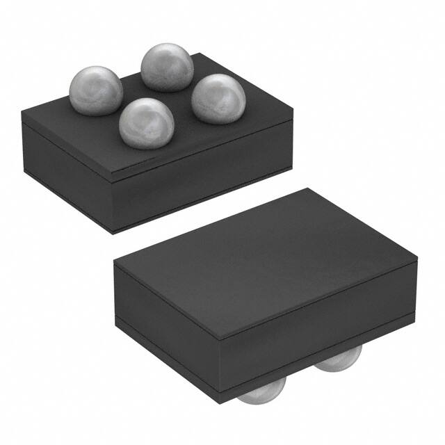
offered in a 4-bump wafer-level package (WLP), and
the minimum operating current is guaranteed to be less
than 1μA. These references feature low temperature
coefficients of less than 20ppm/°C and initial accuracy of
better than 0.2%.
Available with +1.25V, +2.048V, +2.5V, and 3V output
voltages, these references can be used as lowerpower, higher-precision upgrades to the ICL8069, LM385,
LT1004, and LM4040 in much smaller packages. Two
grades are available: A and B. The A grade features a
temperature coefficient of 25ppm/°C over the extended
temperature range of -40°C to +85°C, with an initial
accuracy of 0.2%. Grade B features a temperature
coefficient of 50ppm/°C over the extended temperature
range of -40°C to +85°C, with an initial accuracy of 0.5%.
Their tiny wafer-level packages make these references
ideal for equipment with very small form factors.
Benefits and Features
● Wide Operating Current Range: 1μA to 2mA
● 0.88mm x 1.16mm, 4-Bump WLP
● Initial Voltage Accuracy: 0.2%
● Temperature Coefficient: 20ppm/°C (max)
● Temperature Range: -40°C to +125°C
● Factory-Trimmed Output Voltages: +1.25V, +2.048V,
+2.5V, +3.0V
● Functionally Equivalent to the MAX6006/MAX6007/
MAX6008/MAX6009
Ordering Information appears at end of data sheet.
Simplified Block Diagram
OUT
Applications
●
●
●
●
●
Portable Sensors
Portable Meters
Precision Regulators
A/D and D/A Converters
4mA–20mA Loop-Powered Sensors
MAX6069
GND
19-100064; Rev 1; 10/21
© 2021 Analog Devices, Inc. All rights reserved. Trademarks and registered trademarks are the property of their respective owners.
One Analog Way, Wilmington, MA 01887 U.S.A.
|
Tel: 781.329.4700
|
© 2021 Analog Devices, Inc. All rights reserved.
�MAX6069
1μA Ultra-Tiny Shunt Voltage Reference
Absolute Maximum Ratings
Operating Current (OUT to GND).......................................20mA
Forward Current (GND to OUT)..........................................20mA
Continuous Power Dissipation (Multilayer Board;
derate 9.75mW/°C above +70°C).................................780mW
Operating Temperature Range.......................... -40°C to +125°C
Storage Temperature Range............................. -65°C to +150°C
Junction Temperature.......................................................+150°C
Soldering Temperature (reflow)........................................+260°C
Stresses beyond those listed under “Absolute Maximum Ratings” may cause permanent damage to the device. These are stress ratings only, and functional operation of the device at these
or any other conditions beyond those indicated in the operational sections of the specifications is not implied. Exposure to absolute maximum rating conditions for extended periods may affect
device reliability.
Package Information
WLP
Package Code
W40D1+1
Outline Number
21-100139
Land Pattern Number
Refer to Application Note 1891
Thermal Resistance, Four-Layer Board:
Junction-to-Ambient (θJA)
102.59°C/W
Junction-to-Case (θJC)
N/A
For the latest package outline information and land patterns (footprints), go to www.maximintegrated.com/packages. Note that a “+”,
“#”, or “-” in the package code indicates RoHS status only. Package drawings may show a different suffix character, but the drawing
pertains to the package regardless of RoHS status.
Package thermal resistances were obtained using the method described in JEDEC specification JESD51-7, using a four-layer board.
For detailed information on package thermal considerations, refer to www.maximintegrated.com/thermal-tutorial.
Electrical Characteristics
(TA=-40°C to +125°C, unless otherwise noted., Typical values are at TA = +25°C. (Note 1))
PARAMETER
SYMBOL
CONDITIONS
MIN
TYP
MAX
MAX6069AA (0.2%)
1.2475
1.2500
1.2525
MAX6069AB (0.5%)
1.2438
1.2500
1.2563
0.5
1.0
UNITS
MAX6069A (1.250V)
Reverse Breakdown Voltage
VR
Minimum Operating Current
IRMIN
TA = +25°C,
IR = 1.2µA
VR change < 0.2% from VR at IR = 1.2μA
IR = 1.2μA to 200μA
1
IR = 200μA to 2mA
2.0
Reverse Dynamic
Impedance
IR = 1.2μA to 2mA (Note 2)
1.5
Low-Frequency Noise
IR = 1.2μA, f = 0.1Hz to 10Hz
Reverse Breakdown Change
with Current
www.analog.com
30
V
µA
mV
Ω
µVp-p
Analog Devices │ 2
�MAX6069
1μA Ultra-Tiny Shunt Voltage Reference
Electrical Characteristics (continued)
(TA=-40°C to +125°C, unless otherwise noted., Typical values are at TA = +25°C. (Note 1))
PARAMETER
Temperature Coefficient
(Note 3)
SYMBOL
TC
Long-Term Drift
CONDITIONS
MIN
TYP
MAX
IR = 1.2µA,
MAX6069AA
TA = -40°C to +85°C
20
TA = -40°C to +125°C
25
IR = 1.2µA,
MAX6069AB
TA = -40°C to +85°C
50
TA = -40°C to +125°C
75
1000h at TA = +25°C
Thermal Hysteresis (Note 4)
UNITS
ppm/°C
150
ppm
200
ppm
MAX6069B (2.048V)
Reverse Breakdown Voltage
VR
Minimum Operating Current
IRMIN
TA = +25°C,
IR = 1.2µA
MAX6069BA (0.2%)
2.0439
2.048
2.0521
MAX6069BB (0.5%)
2.0378
2.048
2.0582
0.5
1.0
VR change < 0.2% from VR at IR = 1.2μA
IR = 1.2μA to 200μA
1.3
IR = 200μA to 2mA
2.3
Reverse Dynamic
Impedance
IR = 1.2μA to 2mA (Note 2)
1.8
Low-Frequency Noise
IR = 1.2μA, f = 0.1Hz to 10Hz
Reverse Breakdown Change
with Current
Temperature Coefficient
(Note 3)
Temperature Coefficient
(Note 3)
Temperature Coefficient
(Note 3)
IR = 1.2µA,
MAX6069BA
TC
IR = 1.2µA,
MAX6069BB
Temperature Coefficient
(Note 3)
Long-Term Drift
50
V
µA
mV
Ω
µVp-p
TA = -40°C to +85°C
20
ppm/°C
TA = -40°C to +125°C
25
ppm/°C
TA = -40°C to +85°C
50
ppm/°C
TA = -40°C to +125°C
75
ppm/°C
1000h at TA = +25°C
Thermal Hysteresis (Note 4)
150
ppm
200
ppm
MAX6069C (2.500V)
Reverse Breakdown Voltage
VR
Minimum Operating Current
IRMIN
Reverse Breakdown Change
with Current
Reverse Dynamic
Impedance
www.analog.com
TA = +25°C,
IR = 1.2µA
MAX6069CA (0.2%)
2.4950
2.5000
2.5050
MAX6069CB (0.5%)
2.4875
2.5000
2.5125
0.5
1.0
VR change < 0.2% from VR at IR = 1.2μA
IR = 1.2μA to 200μA
1.5
IR = 200μA to 2mA
2.5
IR = 1.2μA to 2mA (Note 2)
2
V
µA
mV
Ω
Analog Devices │ 3
�MAX6069
1μA Ultra-Tiny Shunt Voltage Reference
Electrical Characteristics (continued)
(TA=-40°C to +125°C, unless otherwise noted., Typical values are at TA = +25°C. (Note 1))
PARAMETER
SYMBOL
Low-Frequency Noise
Temperature Coefficient
(Note 3)
CONDITIONS
MIN
IR = 1.2μA, f = 0.1Hz to 10Hz
TC
Long-Term Drift
TYP
MAX
60
µVp-p
IR = 1.2µA,
MAX6069CA
TA = -40°C to +85°C
20
TA = -40°C to +125°C
25
IR = 1.2µA,
MAX6069CB
TA = -40°C to +85°C
50
TA = -40°C to +125°C
75
1000h at TA = +25°C
Thermal Hysteresis (Note 4)
UNITS
ppm/°C
150
ppm
200
ppm
MAX6069D (3.00V)
Reverse Breakdown Voltage
VR
Minimum Operating Current
IRMIN
TA = +25°C,
IR = 1.2µA
MAX6069DA (0.2%)
2.9940
3.0000
3.0060
MAX6069DB (0.5%)
2.9850
3.0000
3.0150
0.5
1.0
VR change < 0.2% from VR at IR = 1.2μA
IR = 1.2μA to 200μA
1.7
IR = 200μA to 2mA
2.7
Reverse Dynamic
Impedance
IR = 1.2μA to 2mA (Note 2)
2.2
Low-Frequency Noise
IR = 1.2μA, f = 0.1Hz to 10Hz
Reverse Breakdown
Change with Current
Temperature Coefficient
(Note 3)
Long-Term Drift
Thermal Hysteresis (Note 4)
TC
75
µA
mV
Ω
µVp-p
IR = 1.2µA,
MAX6069DA
TA = -40°C to +85°C
20
TA = -40°C to +125°C
25
IR = 1.2µA,
MAX6069DB
TA = -40°C to +85°C
50
TA = -40°C to +125°C
75
1000h at TA = +25°C
V
ppm/°C
150
ppm
200
ppm
Note 1: All units are 100% production tested at TA = +25°C and are guaranteed by design and characterization for
TA = TMIN to TMAX, as specified.
Note 2: This parameter is guaranteed by the “reverse breakdown change with current” test.
Note 3: TC is measured by the “box” method; i.e., (VMAX - VMIN)/(TMAX - TMIN).
Note 4: Thermal hysteresis is defined as the change in the +25°C output voltage after cycling a unit from TMIN to TMAX.
www.analog.com
Analog Devices │ 4
�MAX6069
1μA Ultra-Tiny Shunt Voltage Reference
Typical Operating Characteristics
(TA = +25°C, unless otherwise noted.)
VOUT vs. CURRENT
(MAX6069CA)
TEMPERATURE DRIFT (MAX6069CA)
toc1
1
9
REVERSE-VOLTAGE CHANGE (mV)
REVERSE VOLTAGE CHANGE (mV)
0
-1
-2
-3
-4
-5
-6
-7
toc2
10
8
7
TA = -40°C
6
5
TA = +125°C
4
TA = +85°C
3
2
TA = +25°C
1
-50
-25
0
25
50
75
TEMPERATURE (°C)
MAX6069CA STARTUP
(CL = 0.01µF)
100
0
0.001
125
0.01
0.1
1
10
REVERSE CURRENT (mA)
MAX6069CA PEAK-PEAK
OUTPUT VOLTAGE NOISE
(0.1Hz to 10Hz)
toc3
toc4
1.2µA
IR
0
20µV/div
VOUT
(1V/div)
4ms/div
4s/div
REVERSE DYNAMIC IMPEDANCE
vs. TEMPERATURE (MAX6069CA)
MAX6069CA
OUTPUT IMPEDANCE vs. FREQUENCY
toc5
IMPEDANCE (Ω)
100
CL = 0.01µF
CL = 1µF
10
1
0.1
1
10
100
FREQUENCY (kHz)
www.analog.com
1000
toc6
0.3
REVERSE DYNAMIC IMPEDANCE (Ω)
VOUT = 2.5V,
IR = 6µA,
IR-AC = ±2.5µA
0.2
0.1
0
-50
-25
0
25
50
75
100
125
TEMPERATURE (°C)
Analog Devices │ 5
�MAX6069
1μA Ultra-Tiny Shunt Voltage Reference
Pin Configuration
TOP VIEW
(BUMPS ON BOTTOM)
MAX6069
+ OUT
GND
A1
A2
B1
B2
OUT
GND
WLP
Pin Description
PIN
NAME
FUNCTION
A1
OUT
Output Voltage. Bias OUT with a pullup resistor to a potential greater than OUT.
Bypass OUT to GND with a 0.01µF or larger capacitor.
A2
GND
Ground
B1
OUT
Output Voltage. B1 is shorted to A1 internally.
B2
GND
Ground. B2 is shorted to A2 internally.
Detailed Description
The MAX6069 family consists of precision, twoterminal, shunt bandgap voltage references. On-chip,
thin-film resistors are laser-trimmed to provide 0.2% output
voltage accuracies. Voltages of +1.25V, +2.048V, +2.5V,
and +3.0V are available in a space-saving 4-bump WLP.
Applications Information
Output/Load Capacitance
Bypass OUT to GND with a 0.01μF or larger capacitor.
In applications where the load or the supply can experience
step changes, additional capacitance will reduce the
amount of overshoot (or undershoot) and assist the
circuit’s transient response.
www.analog.com
Output Voltage Hysteresis
Output voltage hysteresis is the change in the output
voltage at TA = +25°C before and after the device is cycled
over its entire operating temperature range. Hysteresis is
caused by differential package stress appearing across
the bandgap core transistors. The temperature hysteresis
value is typically less than 200ppm.
Turn-On Time
The output capacitance and bias current of the MAX6069
greatly affect turn-on settling time. In the Typical Operating
Characteristics, turn-on time is shown with a 10nF output capacitor and a 1.2μA bias current. Under these
conditions, the MAX6069 settles in about 4ms. Settling
time linearly decreases in proportion to the circuit’s bias
current.
Analog Devices │ 6
�MAX6069
1μA Ultra-Tiny Shunt Voltage Reference
Typical Application Circuits
Shunt Regulator Connection
In the typical shunt regulator connection shown here, RBIAS sets the current through the load (IL) and the current through
the shunt regulator(IR). There are two worst-case situations that RBIAS needs to be sized for:
1) RBIAS must be small enough that when VS (supply voltage) is at its minimum and IL is at its maximum, IR is equal to
at least the minimum operating current of the shunt regulator.
2) RBIAS must be large enough that when VS is at its maximum and IL is at its minimum, IR is < 2mA.
VS
RBIAS
VR
MAX6069
IR + IL
IL
10nF
IR
RBIAS =
Precision Current Sink
VOUT
VS - VR
IL + IR
Precision Current Source
MAX6069C
MAX6069C
R1
200kΩ
R1
200kΩ
-10V
IOUT
R2
-1V to -7V
IOUT =
www.analog.com
2.5V
+10V
IOUT
+1V TO +7V
IOUT =
R2
2.5V
R2
R2
Analog Devices │ 7
�MAX6069
1μA Ultra-Tiny Shunt Voltage Reference
Ordering Information
OUTPUT
VOLTAGE (V)
INITIAL
ACCURACY (%)
TEMP COEFFICIENT
(PPM/°C)
PIN-PACKAGE
TOP
MARK
MAX6069AAAWS+*
1.250
0.2
20
4 WLP
+AM
MAX6069AAAWS+T*
1.250
0.2
20
4 WLP
+AM
MAX6069ABAWS+*
1.250
0.5
50
4 WLP
+AN
MAX6069ABAWS+T*
1.250
0.5
50
4 WLP
+AN
MAX6069BAAWS+
2.048
0.2
20
4 WLP
+AO
MAX6069BAAWS+T
2.048
0.2
20
4 WLP
+AO
MAX6069BBAWS+*
2.048
0.5
50
4 WLP
+AP
MAX6069BBAWS+T*
2.048
0.5
50
4 WLP
+AP
MAX6069CAAWS+
2.500
0.2
20
4 WLP
+AQ
MAX6069CAAWS+T
2.500
0.2
20
4 WLP
+AQ
MAX6069CBAWS+
2.500
0.5
50
4 WLP
+AR
MAX6069CBAWS+T
2.500
0.5
50
4 WLP
+AR
MAX6069DAAWS+*
3.000
0.2
20
4 WLP
+AS
MAX6069DAAWS+T*
3.000
0.2
20
4 WLP
+AS
MAX6069DBAWS+*
3.000
0.5
50
4 WLP
+AT
MAX6069DBAWS+T*
3.000
0.5
50
4 WLP
+AT
PART NUMBER
+Denotes a lead(Pb)-free/RoHS-compliant package.
T = Tape and reel.
*Future product—contact factory for availability.
www.analog.com
Analog Devices │ 8
�MAX6069
1μA Ultra-Tiny Shunt Voltage Reference
Revision History
REVISION
NUMBER
REVISION
DATE
0
6/17
Initial release
1
10/21
Updated Electrical Characteristics, Precision Current Source figure, and Ordering
Information
DESCRIPTION
PAGES
CHANGED
—
3, 4, 7, 8
Information furnished by Analog Devices is believed to be accurate and reliable. However, no responsibility is
assumed by Analog Devices for its use, nor for any infringements of patents or other rights of third parties that
may result from its use.Specifications subject to change without notice. No license is granted by implicationor
otherwise under any patent or patent rights of Analog Devices. Trademarks andregistered trademarks are the
property of their respective owners.
w w w . a n a l o g . c o m
Analog Devices │ 9
�


 工商网监
湘ICP备2023018690号
工商网监
湘ICP备2023018690号
