19-1695; Rev 2; 12/05
Quad Voltage Monitor in µMAX Package
The MAX6338 quad voltage monitor is capable of monitoring up to four supplies without any external components. A variety of factory-trimmed threshold voltages
and supply tolerances are available to optimize the
MAX6338 for specific applications. The selection
includes input options for monitoring +5.0V, +3.3V,
+3.0V, +2.5V, +1.8V, and -5.0V voltages. An additional
high-input impedance comparator option can be used
as an adjustable voltage monitor, general-purpose comparator, or digital level translator.
Each of the monitored voltages is available with trip
thresholds to support power-supply tolerances of either
5% or 10% below the nominal voltage. An internal
bandgap reference ensures accurate trip thresholds
across the extended (-40°C to +85°C) operating temperature range.
The MAX6338 consumes 25µA (typ) supply current and
operates with supply voltages from +2.5V to +5.5V. An
internal undervoltage lockout circuit forces all four digital
outputs low when VCC drops below the minimum operating voltage. The four digital outputs all have weak internal pull-ups to VCC, allowing wire-ORed connection.
Each input threshold voltage has an independent output.
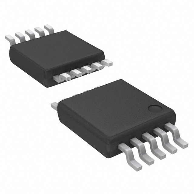
The MAX6338 is available in a 10-pin µMAX® package.
________________________Applications
Features
♦ Monitors Four Voltages (Factory Programmed or
User Adjustable)
+5.0V, +3.3V, +3.0V, +2.5V, +1.8V, -5.0V
(nominal) or User-Adjustable Settings
♦ Low 25µA Supply Current
♦ Four Independent, Open-Drain, Active-Low
Outputs
♦ +2.5V to +5.5V Supply Voltage Range
♦ Guaranteed from -40°C to +85°C
♦ No External Components Required
♦ Small 10-Pin µMAX Package
Ordering Information
PART
TEMP RANGE
PIN-PACKAGE
MAX6338_UB*
-40°C to +85°C
10 µMAX
*Insert the desired letter from the Selector Guide into the blank
to complete the part number.
Devices are available in both leaded and lead-free packaging.
Specify lead free by adding the + symbol at the end of the part
number when ordering.
Selector Guide
NOMINAL INPUT VOLTAGE
PART
IN1
(V)
IN2
(V)
IN3
(V)
IN4
(V)
SUPPLY
TOLERANCE
(%)
Adj*
10
Telecommunications
High-End Printers
MAX6338AUB
5
3.3
2.5
Desktop and Notebook Computers
MAX6338BUB
5
3.3
2.5†
Adj*
5
Data Storage Equipment
MAX6338CUB
5
3.3
1.8
Adj*
10
Networking Equipment
MAX6338DUB
5
3.3
1.8†
Adj*
5
Industrial Equipment
MAX6338EUB
5
3.0
2.5
Adj*
10
MAX6338FUB
5
3.0
2.5†
Adj*
5
MAX6338GUB
5
3.0
1.8
Adj*
10
MAX6338HUB
5
3.0
1.8†
Adj*
5
MAX6338IUB
5
3.3
2.5
1.8
10
MAX6338JUB
5
3.3
2.5†
1.8†
5
MAX6338KUB
Adj*
3.3
2.5
Adj*
10
MAX6338LUB
Adj*
3.3
2.5†
Adj*
5
MAX6338MUB
5
3.0
Adj*
-5
10
Set-Top Boxes
Pin Configuration
TOP VIEW
IN1 1
IN2
2
IN3
3
IN4
4
GND
5
10 VCC
MAX6338
9
OUT1
8
OUT2
MAX6338NUB
5
3.0
Adj*
-5
5
7
OUT3
MAX6338OUB
5
3.3
Adj*
-5
10
6
OUT4
MAX6338PUB
5
3.3
Adj*
-5
5
µMAX
µMAX is a registered trademark of Maxim Integrated Products, Inc.
*Adjustable voltage based on +1.23V internal threshold. External
threshold voltage can be set using an external resistor-divider.
† Nominal input voltages for 1.8V and 2.5V are specified for 10%
tolerances
________________________________________________________________ Maxim Integrated Products
For pricing, delivery, and ordering information, please contact Maxim/Dallas Direct! at
1-888-629-4642, or visit Maxim’s website at www.maxim-ic.com.
1
MAX6338
General Description
�MAX6338
Quad Voltage Monitor in µMAX Package
ABSOLUTE MAXIMUM RATINGS
Terminal Voltage (with respect to GND)
VCC ......................................................................-0.3V to +6V
Output Voltages (OUT_) ...........................................-0.3V to +6V
Input Voltages (IN_) (except -5V).............................-0.3V to +6V
Input Voltage (-5V input) ..........................................-6V to +0.3V
Continuous OUT_ Current...................................................20mA
Continuous Power Dissipation (TA = +70°C)
10-pin µMAX (derate 5.6mW/°C above +70°C) ..........444mW
Operating Temperature Range ...........................-40°C to +85°C
Storage Temperature Range .............................-65°C to +150°C
Junction Temperature ......................................................+150°C
Lead Temperature (soldering, 10s) .................................+300°C
Stresses beyond those listed under “Absolute Maximum Ratings” may cause permanent damage to the device. These are stress ratings only, and functional
operation of the device at these or any other conditions beyond those indicated in the operational sections of the specifications is not implied. Exposure to
absolute maximum rating conditions for extended periods may affect device reliability.
ELECTRICAL CHARACTERISTICS
(VCC = +2.5V to +5.5V, TA= -40°C to +85°C, unless otherwise noted. Typical values are at TA= +25°C and VCC = +5V, unless otherwise noted.) (Note 1)
PARAMETER
SYMBOL
Supply Voltage Range
VCC
Supply Current
ICC
Input Current (Note 2)
IIN_
CONDITIONS
MIN
TYP
+2.5
MAX
UNITS
+5.5
V
VCC = +3V
25
50
VCC = +5V
35
65
VIN_ = input threshold voltage
(+1.8V, +2.5V, +3.0V, +3.3V, +5.0V)
25
40
VIN_ = 0 to VCC
(input threshold voltage =1.23V)
-0.1
VIN_ = -5V
(input threshold voltage = -5V)
+0.1
µA
µA
-10
-20
4.63
4.75
V
+5.0V (-5%) Threshold
VTH
VIN decreasing
4.5
+5.0V (-10%) Threshold
VTH
VIN decreasing
4.25
4.38
4.50
V
+3.3V (-5%) Threshold
VTH
VIN decreasing
3.0
3.08
3.15
V
+3.3V (-10%) Threshold
VTH
VIN decreasing
2.85
2.93
3.00
V
+3.0V (-5%) Threshold
VTH
VIN decreasing
2.7
2.78
2.85
V
+3.0V (-10%) Threshold
VTH
VIN decreasing
2.55
2.63
2.70
V
+2.5V (-10%) Threshold
VTH
VIN decreasing
2.13
2.19
2.25
V
+1.8V (-10%) Threshold
VTH
VIN decreasing
1.53
1.58
1.62
V
-5.0V (+5%) Threshold
VTH
VIN increasing
-4.75
-4.63
-4.50
V
-5.0V (+10%) Threshold
VTH
VIN increasing
-4.5
-4.38
-4.25
V
Adjustable Threshold
VTH
VIN decreasing
1.20
1.23
1.26
V
Threshold Voltage Temperature
Coefficient
Threshold Hysteresis
VTHYST
Propagation Delay
tpd
Output Low Voltage
VOL
Output High Voltage
VOH
VIN_ = VTH to (VTH - 50mV) or
VTH to (VTH - 50mV)
60
ppm/°C
0.3
%
20
µs
VCC = 5V, ISINK = 2mA
0.4
VCC = 2.5V, ISINK = 1.2mA
0.4
VCC = 1V, ISINK = 50µA
VCC > 2.5V, ISOURCE = 6µA (minimum)
0.4
0.8 x VCC
Note 1: 100% production tested at +25°C. Overtemperature limits guaranteed by design.
Note 2: Guaranteed by design.
2
V
_______________________________________________________________________________________
V
�Quad Voltage Monitor in µMAX Package
NORMALIZED THRESHOLD ERROR
vs. SUPPLY VOLTAGE
30
25
TA = -40°C
20
15
0.04
0.02
0
-0.02
3.0
3.5
4.0
4.5
5.0
-0.1
-0.2
-0.3
2.5
5.5
0
NORMALIZED TO +5V
-0.04
3.0
3.5
4.0
4.5
5.0
5.5
-40
-20
0
20
40
60
SUPPLY VOLTAGE (V)
TEMPERATURE (°C)
OUTPUT-VOLTAGE LOW
vs. SINK CURRENT
PROPAGATION DELAY
(WITH 100mV OVERDRIVE)
PROPAGATION DELAY
(WITH 20mV OVERDRIVE)
0.6
VCC = 5V
0.5
0.4
80
MAX6338-06
SUPPLY VOLTAGE (V)
MAX6338-04
2.5
OUTPUT-VOLTAGE LOW (V)
0.06
-0.06
10
VCC = +5V
NORMALIZED THRESHOLD (%)
35
0.1
MAX6338-02
MAX6338-01
TA = +25°C
TA = +85°C
0.08
MAX6338-05
SUPPLY CURRENT (µA)
40
0.10
NORMALIZED THRESHOLD ERROR (%)
45
NORMALIZE THRESHOLD
vs. TEMPERATURE
MAX6338-03
SUPPLY CURRENT
vs. SUPPLY VOLTAGE
IN_
50mV/div
IN_
20mV/div
OUT_
2V/div
OUT_
2V/div
TA = +25°C
0.3
TA = +85°C
0.2
TA = -40°C
0.1
0
0
1
2
3
4
5
6
7
8
9
10
10µs/div
10µs/div
SINK CURRENT (mA)
_______________________________________________________________________________________
3
MAX6338
Typical Operating Characteristics
(VCC = +5V, TA = +25°C, unless otherwise noted.)
�Quad Voltage Monitor in µMAX Package
MAX6338
Pin Description
PIN
NAME
FUNCTION
1
IN1
Input Voltage 1. See the Selector Guide for monitored voltages.
2
IN2
Input Voltage 2. See the Selector Guide for monitored voltages.
3
IN3
Input Voltage 3. See the Selector Guide for monitored voltages.
4
IN4
Input Voltage 4. See the Selector Guide for monitored voltages.
5
GND
Ground
6
OUT4
Output 4. OUT4 goes low when VIN4 falls below its absolute threshold. OUT4 is open drain with a 10µA
internal pullup to VCC.
7
OUT3
Output 3. OUT3 goes low when VIN3 falls below its absolute threshold. OUT3 is open drain with a 10µA
internal pullup to VCC.
8
OUT2
Output 2. OUT2 goes low when VIN2 falls below its absolute threshold. OUT2 is open drain with a 10µA
internal pullup to VCC.
9
OUT1
Output 1. OUT1 goes low when VIN1 falls below its absolute threshold. OUT1 is open drain with a 10µA
internal pullup to VCC.
10
VCC
Power Supply. Connect VCC to a +2.5V to +5.5V supply. An undervoltage lockout circuit forces all OUT_
pins low when VCC drops below 2.5V.
_______________Detailed Description
The MAX6338 is a low-power (25µA), quad voltage
monitor designed for multivoltage systems. Preset voltage options for +5.0V, +3.3V, +3.0V, +2.5V, +1.8V, and
-5.0V make these quad monitors ideal for applications
such as telecommunications, desktop and notebook
computers, high-end printers, data storage equipment,
and networking equipment.
The MAX6338 has an internally trimmed threshold that
minimizes or eliminates the need for external components. The four open-drain outputs have weak (10µA)
internal pullups to VCC, allowing them to interface easily
with other logic devices. The MAX6338 can monitor
power supplies with either 5% or 10% tolerance specifications, depending on the selected version. An additional high-input-impedance comparator option can be
used as an adjustable voltage monitor, general-purpose comparator, or digital level translator.
The weak internal pullups can be overdriven by external
pullups to any voltage from 0 to +5.5V. Internal circuitry
prevents current flow from the external pullup voltage to
VCC. The outputs can be wire-ORed for a single “power
good” signal.
The MAX6338 has either one or two auxiliary inputs and
two or three factory-programmed threshold voltages, or
four fixed voltages. The inverting input of all compara4
tors is connected to a 1.23V bandgap reference for all
positive voltages. The noninverting terminals are accessible through internal resistive voltage-dividers with
preset factory threshold voltages. In the case of auxiliary (AUX) input, the positive terminal of the comparator
is accessible directly for setting the threshold for the
monitored voltage.
When any of the inputs (IN1–IN4) are higher than the
threshold level, the output is high. The output goes low
as the input drops below the threshold voltage monitor.
The undervoltage lockout circuitry remains active and
the outputs remain low with VCC down to 1V (Figure 1).
Applications Information
Hysteresis
When the voltage on one comparator input is at or near
the voltage on the other input, ambient noise generally
causes the comparator output to oscillate. The most
common way to eliminate this problem is through hysteresis. When the two comparator input voltages are
equal, hysteresis causes one comparator input voltage
to move quickly past the other, thus taking the input out
of the region where oscillation occurs. Standard comparators require hysteresis to be added through the
use of external resistors. The external resistive network
usually provides a positive feedback to the input in
order to cause a jump in the threshold voltage when
_______________________________________________________________________________________
�Quad Voltage Monitor in µMAX Package
MAX6338
VCC
MAX6338M/N/O/P
IN1
OUT1
VCC
IN2
OUT2
VCC
IN3*
(AUX)*
OUT3
VCC
IN4
(-5V)
OUT4
VREF
REFERENCE
VCC
UNDERVOLTAGE LOCKOUT
*SEE AUXILIARY INPUT SECTION.
Figure 1. Functional Diagram
_______________________________________________________________________________________
5
�MAX6338
Quad Voltage Monitor in µMAX Package
+5V
+5V
0.1µF*
VCC
V1
IN1
V2
IN2
V3
IN3
V4
IN4
MAX6338
VCC
VIN (+5V)
D1
IN1
IN2
OUT1
OUT1
MAX6338
D2
OUT2
D3
OUT2
IN3
OUT3
IN4
OUT4
OUT3
D4
OUT4
GND
GND
*OPTIONAL
Figure 2. Quad Undervoltage Detector with LED Indicators
+5V
VTH1 = 1 + R2 VREF
R1
(
)
OUT1
VCC
R2
VREF = 1.23V
Figure 3. VCC Bar Graph Monitoring
IN1
R1
IN2
VTH1
OUT1
MAX6338HUB
OUT2
OUT1
INPUT
IN3
OUT3
OUT4
VTH4
R4
IN4
R3
OUT4
GND
VTH4 = 1 + R4 VREF
R3
(
)
OUT
∆VTH
Figure 4. Window Detection
Figure 5. Output Response of Window Detector Circuit
output toggles in one direction or the other. These
resistors are not required when using the MAX6338
because hysteresis is built into the device. MAX6338
hysteresis is typically 0.3%.
The MAX6338 can also be used in applications such as
system supervisory monitoring, multivoltage level
detection, and VCC bar graph monitoring (Figure 3).
Undervoltage Detection Circuit
A window detector circuit uses two auxiliary inputs in a
configuration such as the one shown in Figure 4.
External resistors R1–R4 set the two threshold voltages
(VTH1 and VTH4) of the window detector circuit. Window
width (∆VTH) is the difference between the threshold
voltages (Figure 5).
The open-drain outputs of the MAX6338 can be configured to detect an undervoltage condition. Figure 2
shows a configuration where a low at a comparator output indicates an undervoltage condition, which in turn
causes an LED to light.
6
Window Detection
_______________________________________________________________________________________
�Quad Voltage Monitor in µMAX Package
R1
The unused inputs (except the auxiliary) are internally
connected to ground through the lower resistors of the
threshold-setting resistor pairs. The auxiliary (AUX)
input, however, must be connected to either ground or
VCC if unused.
R2
The MAX6338 operates from a single +2.5V to +5.5V
supply. In noisy applications, connect a 0.1µF capacitor on the supply voltage line close to VCC pin for
bypassing.
Power-Supply Bypassing and Grounding
VREF = 1.23V
R1 = R2
Chip Information
INTH
- 1)
( V1.23
TRANSISTOR COUNT: 620
PROCESS: BiCMOS
Figure 6. Setting the Auxiliary Monitor
Auxiliary Input
The adjustable voltage monitor is comparable to an
internal reference of 1.23V as shown in Figure 6. To set
the desired trip level of monitored supply, V INTH ,
choose: R1 = R2 [(VINTH / 1.23) - 1)]. For example, for a
voltage detection at 4.5V (assume R2 = 100kΩ), R1 =
265kΩ.
Typical Operating Circuit
+2.5V TO +5.5V
(MAY BE ONE OF THE MONITORED VOLTAGES)
VCC
IN1
SUPPLIES
TO BE
MONITORED
MAX6338
OUT1
IN2
OUT2
IN3
OUT3
IN4
OUT4
SYSTEM
LOGIC
µP
GND
_______________________________________________________________________________________
7
MAX6338
Unused Inputs
VINTH
�Package Information
(The package drawing(s) in this data sheet may not reflect the most current specifications. For the latest package outline information,
go to www.maxim-ic.com/packages.)
e
10LUMAX.EPS
MAX6338
Quad Voltage Monitor in µMAX Package
4X S
10
10
INCHES
H
Ø0.50±0.1
0.6±0.1
1
1
0.6±0.1
BOTTOM VIEW
TOP VIEW
D2
MILLIMETERS
MAX
DIM MIN
0.043
A
0.006
A1
0.002
A2
0.030
0.037
D1
0.120
0.116
0.118
D2
0.114
E1
0.116
0.120
0.118
E2
0.114
0.199
H
0.187
L
0.0157 0.0275
L1
0.037 REF
b
0.007
0.0106
e
0.0197 BSC
c
0.0035 0.0078
0.0196 REF
S
α
0°
6°
MAX
MIN
1.10
0.15
0.05
0.75
0.95
3.05
2.95
2.89
3.00
3.05
2.95
2.89
3.00
4.75
5.05
0.40
0.70
0.940 REF
0.177
0.270
0.500 BSC
0.090
0.200
0.498 REF
0°
6°
E2
GAGE PLANE
A2
c
A
b
A1
α
E1
L
D1
L1
FRONT VIEW
SIDE VIEW
PROPRIETARY INFORMATION
TITLE:
PACKAGE OUTLINE, 10L uMAX/uSOP
APPROVAL
DOCUMENT CONTROL NO.
21-0061
REV.
1
1
Maxim cannot assume responsibility for use of any circuitry other than circuitry entirely embodied in a Maxim product. No circuit patent licenses are
implied. Maxim reserves the right to change the circuitry and specifications without notice at any time.
8 _____________________Maxim Integrated Products, 120 San Gabriel Drive, Sunnyvale, CA 94086 408-737-7600
© 2005 Maxim Integrated Products
Printed USA
is a registered trademark of Maxim Integrated Products, Inc.
�


 工商网监
湘ICP备2023018690号
工商网监
湘ICP备2023018690号
