MAX6340/
MAX6421–MAX6426
Low-Power, SC70/SOT µP Reset Circuits with
Capacitor-Adjustable Reset Timeout Delay
General Description
The MAX6340/MAX6421–MAX6426 low-power microprocessor supervisor circuits monitor system voltages
from 1.6V to 5V. These devices perform a single function:
they assert a reset signal whenever the VCC supply voltage falls below its reset threshold. The reset output
remains asserted for the reset timeout period after VCC
rises above the reset threshold. The reset timeout is externally set by a capacitor to provide more flexibility.
The MAX6421/MAX6424 have an active-low, pushpull reset output. The MAX6422 has an active-high,
push-pull reset output and the MAX6340/MAX6423/
MAX6425/MAX6426 have an active-low, open-drain
reset output. The MAX6421/MAX6422/MAX6423 are
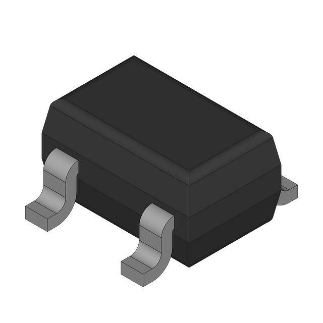
offered in 4-pin SC70 or SOT143 packages. The
MAX6340/MAX6424/MAX6425/MAX6426 are available
in 5-pin SOT23-5 packages.
Features
o Monitor System Voltages from 1.6V to 5V
o Capacitor-Adjustable Reset Timeout Period
o Low Quiescent Current (1.6µA typ)
o Three RESET Output Options
Push-Pull RESET
Push-Pull RESET
Open-Drain RESET
o Guaranteed Reset Valid to VCC = 1V
o Immune to Short VCC Transients
o Small 4-Pin SC70, 4-Pin SOT143, and 5-Pin SOT23
Packages
o MAX6340 Pin Compatible with LP3470
o MAX6424/MAX6425 Pin Compatible with
NCP300–NCP303, MC33464/MC33465,
S807/S808/S809, and RN5VD
o MAX6426 Pin Compatible with PST92XX
Applications
Portable Equipment
Battery-Powered Computers/Controllers
Ordering Information
PART
TEMP RANGE
PIN-PACKAGE
MAX6340UK_ _-T
-40°C to +125°C
5 SOT23-5
Automotive
MAX6340UK_ _/V+T
-40°C to +125°C
5 SOT23-5
Medical Equipment
MAX6421XS_ _-T
-40°C to +125°C
4 SC70-4
Intelligent Instruments
MAX6421US_ _-T
-40°C to +125°C
4 SOT143-4
Embedded Controllers
MAX6422XS_ _-T
-40°C to +125°C
4 SC70-4
Critical µP Monitoring
MAX6422US_ _-T
-40°C to +125°C
4 SOT143-4
MAX6423XS_ _-T
-40°C to +125°C
4 SC70-4
MAX6423US_ _-T
-40°C to +125°C
4 SOT143-4
MAX6424UK_ _-T
-40°C to +125°C
5 SOT23-5
MAX6425UK_ _-T
-40°C to +125°C
5 SOT23-5
MAX6426UK_ _-T
-40°C to +125°C
5 SOT23-5
Set-Top Boxes
Computers
Typical Operating Circuit appears at end of data sheet.
Pin Configurations
TOP VIEW
+
VCC 1
GND 2
MAX6421X
MAX6422X
MAX6423X
4
RESET
(RESET)
3
SRT
SC70
( ) ARE FOR THE MAX6422
Pin Configurations continued at end of data sheet.
Note: The MAX6340/MAX6421–MAX6426 are available with
factory-trimmed reset thresholds from 1.575V to 5.0V in approximately 0.1V increments. Insert the desired nominal reset threshold suffix (from Table 1) into the blanks. There are 50 standard
versions with a required order increment of 2500 pieces. Sample
stock is generally held on standard versions only (see Standard
Versions Table). Required order increment is 10,000 pieces for
nonstandard versions. Contact factory for availability. All devices
are available in tape-and-reel only.
Devices are available in both leaded and lead-free packaging.
Specify lead-free by replacing "-T" with "+T" when ordering.
/V denotes an automotive qualified part.
Typical Operating Circuit appears at end of data sheet.
Selector Guide appears at end of data sheet.
For pricing, delivery, and ordering information, please contact Maxim Direct
at 1-888-629-4642, or visit Maxim’s website at www.maximintegrated.com.
19-2440; Rev 5; 12/13
�MAX6340/
MAX6421–MAX6426
Low-Power, SC70/SOT µP Reset Circuits with
Capacitor-Adjustable Reset Timeout Delay
ABSOLUTE MAXIMUM RATINGS
Continuous Power Dissipation (TA = +70°C)
4-Pin SC70 (derate 3.1mW/°C above +70°C) ..............245mW
4-Pin SOT143 (derate 4mW/°C above +70°C).............320mW
5-Pin SOT23 (derate 7.1mW/°C above +70°C)............571mW
Operating Temperature Range .........................-40°C to +125°C
Storage Temperature Range .............................-65°C to +150°C
Junction Temperature ......................................................+150°C
Lead Temperature (soldering, 10s) .................................+300°C
All Voltages Referenced to GND
VCC ........................................................................-0.3V to +6.0V
SRT, RESET, RESET (push-pull).................-0.3V to (VCC + 0.3V)
RESET (open drain)...............................................-0.3V to +6.0V
Input Current (all pins)......................................................±20mA
Output Current (RESET, RESET) ......................................±20mA
Stresses beyond those listed under “Absolute Maximum Ratings” may cause permanent damage to the device. These are stress ratings only, and functional
operation of the device at these or any other conditions beyond those indicated in the operational sections of the specifications is not implied. Exposure to
absolute maximum rating conditions for extended periods may affect device reliability.
ELECTRICAL CHARACTERISTICS
(VCC = 1V to 5.5V, TA = TMIN to TMAX, unless otherwise specified. Typical values are at VCC = 5V and TA = +25°C.) (Note 1)
PARAMETER
Supply Voltage Range
Supply Current
VCC Reset Threshold Accuracy
Hysteresis
SYMBOL
ICC
VTH
tRD
Reset Timeout Period
tRP
VSRT Ramp Threshold
IRAMP
VTH-RAMP
RAMP Threshold Hysteresis
RESET Output Voltage Low
RESET Output Voltage High,
Push-Pull
RESET Output Leakage Current,
Open-Drain
RESET Output Voltage High
RESET Output Voltage Low
MIN
ILKG
VOH
VOL
UNITS
5.5
V
2.5
4.2
VCC ≤ 3.3V
1.9
3.4
VCC ≤ 2.0V
1.6
2.5
TA = +25°C
VTH - 1.5%
VTH + 1.5%
TA = -40°C to +125°C
VTH - 2.5%
VTH + 2.5%
VCC falling at 1mV/µs
CSRT = 1500pF
3.00
CSRT = 0
µA
V
4 x VTH
mV
80
µs
4.375
5.75
0.275
ms
VSRT = 0 to 0.65V; VCC = 1.6V to 5V
240
VCC = 1.6V to 5V (VRAMP rising)
0.65
V
33
mV
nA
VCC ≥ 1.0V, ISINK = 50µA
0.3
VCC ≥ 2.7V, ISINK = 1.2mA
0.3
VCC ≥ 4.5V, ISINK = 3.2mA
0.4
VCC ≥ 1.8V, ISOURCE = 200µA
VOH
MAX
VCC ≤ 5.0V
VRAMP falling threshold
VOL
TYP
1.0
VHYST
VCC to Reset Delay
VSRT Ramp Current
CONDITIONS
VCC
V
0.8 x VCC
VCC ≥ 2.25V, ISOURCE = 500µA
0.8 x VCC
VCC ≥ 4.5V, ISOURCE = 800µA
0.8 x VCC
VCC > VTH, reset not asserted
V
1.0
VCC ≥ 1.0V, ISOURCE = 1µA
0.8 x VCC
VCC ≥ 1.8V, ISOURCE = 150µA
0.8 x VCC
VCC ≥ 2.7V, ISOURCE = 500µA
0.8 x VCC
VCC ≥ 4.5V, ISOURCE = 800µA
0.8 x VCC
µA
V
VCC ≥ 1.8V, ISINK = 500µA
0.3
VCC ≥ 2.7V, ISINK = 1.2mA
0.3
VCC ≥ 4.5V, ISINK = 3.2mA
0.4
V
Note 1: Devices production tested at +25°C. Overtemperature limits are guaranteed by design.
2
Maxim Integrated
�MAX6340/
MAX6421–MAX6426
Low-Power, SC70/SOT µP Reset Circuits with
Capacitor-Adjustable Reset Timeout Delay
Typical Operating Characteristics
(VCC = 5V, CSRT = 1500pF, TA = +25°C, unless otherwise noted.)
TA = +25°C
2.5
2.0
TA = -40°C
1.5
1.0
1000
100
10
1
4.30
CSRT = 1500pF
RESET TIMEOUT PERIOD (ms)
3.0
MAX6421/26 toc02
TA = +125°C
10,000
RESET TIMEOUT PERIOD (ms)
SUPPLY CURRENT (μA)
MAX6421/26 toc01
4.0
3.5
RESET TIMEOUT PERIOD
vs. TEMPERATURE
RESET TIMEOUT PERIOD vs. CSRT
4.25
MAX6421/26 toc03
SUPPLY CURRENT
vs. SUPPLY VOLTAGE
4.20
4.15
0.5
0
1
2
3
4
5
4.10
0.01
0.1
1
10
-50
1000
100
0
25
50
75
100
CSRT (nF)
TEMPERATURE (°C)
RESET TIMEOUT PERIOD
vs. TEMPERATURE
MAXIMUM TRANSIENT DURATION
vs. RESET THRESHOLD OVERDRIVE
VCC TO RESET DELAY
vs. TEMPERATURE (VCC FALLING)
450
400
350
300
125
100
RESET OCCURS
ABOVE THE CURVE
75
50
250
25
200
0
VCC FALLING AT 1mVμs
150
0
50
25
75
100
125
140
130
120
110
100
90
VTH = 2.95V
-25
80
0
TEMPERATURE (°C)
200
400
600
800
1000
-50
-25
0
RESET THRESHOLD OVERDRIVE (mV)
POWER-UP/POWER-DOWN
CHARACTERISTIC
1V/div
RESET
1V/div
100
125
MAX6421/26 toc08
1.006
NORMALIZED RESET THRESHOLD
VCC
25
75
50
TEMPERATURE (°C)
NORMALIZED RESET THRESHOLD
vs. TEMPERATURE
MAX6421/26 toc07
VTH = 1.6V
125
MAX6421/26 toc06
150
160
VCC TO RESET DELAY (μs)
500
MAX6421/26 toc05
550
175
TRANSIENT DURATION (μs)
CSRT = 0
-50
-25
SUPPLY VOLTAGE (V)
600
RESET TIMEOUT PERIOD (μs)
0.1
0.001
6
MAX6421/26 toc04
0
1.004
1.002
1.000
0.998
0.996
0.994
400μs/div
-50
-25
0
25
50
75
100
125
TEMPERATURE (°C)
Maxim Integrated
3
�MAX6340/
MAX6421–MAX6426
Low-Power, SC70/SOT µP Reset Circuits with
Capacitor-Adjustable Reset Timeout Delay
Pin Description
PIN
MAX6340
SOT23
1
MAX6421
MAX6422
MAX6423
SOT143
3
SC70
3
MAX6424
MAX6425
MAX6426
SOT23
SOT23
NAME
5
1
SRT
FUNCTION
Set Reset Timeout Input. Connect a capacitor between SRT
and ground to set the timeout period. Determine the period as
follows: tRP = 2.73 ✕ 106 ✕ CSRT + 275µs with tRP in seconds
and CSRT in farads.
2
1
2
3
2, 3
GND
Ground
3
—
—
4
—
N.C.
Not Internally Connected. Can be connected to GND.
4
2
1
2
5
VCC
Supply Voltage and Reset Threshold Monitor Input
5
1
4
—
4
RESET
RESET changes from high to low whenever VCC drops below
the selected reset threshold voltage. RESET remains low for
the reset timeout period after VCC exceeds the reset
threshold.
RESET
RESET changes from low to high whenever VCC drops below
the selected reset threshold voltage. RESET remains high for
the reset timeout period after VCC exceeds the reset
threshold.
4
—
—
Detailed Description
Reset Output
The reset output is typically connected to the reset input
of a µP. A µP’s reset input starts or restarts the µP in a
known state. The MAX6340/MAX6421–MAX6426 µP
supervisory circuits provide the reset logic to prevent
code-execution errors during power-up, power-down,
and brownout conditions (see Typical Operating
Characteristics).
RESET changes from high to low whenever VCC drops
below the threshold voltage. Once VCC exceeds the
threshold voltage, RESET remains low for the capacitoradjustable reset timeout period.
The MAX6422 active-high RESET output is the inverse
logic of the active-low RESET output. All device outputs
are guaranteed valid for VCC > 1V.
The MAX6340/MAX6423/MAX6425/MAX6426 are opendrain RESET outputs. Connect an external pullup resistor to any supply from 0 to 5.5V. Select a resistor value
large enough to register a logic low when RESET is
asserted and small enough to register a logic high
while supplying all input current and leakage paths
connected to the RESET line. A 10kΩ to 100kΩ pullup
is sufficient in most applications.
4
3.3V
VCC
LASER-TRIMMED
RESISTORS
5.0V
10kΩ
VREF
RESET
5V
SYSTEM
SRT
N
RESET
TIMEOUT
CSRT
MAX6340
MAX6423
MAX6425
MAX6426
GND
Figure 1. MAX6340/MAX6423/MAX6425/MAX6426 Open-Drain
RESET Output Allows Use with Multiple Supplies
Maxim Integrated
�MAX6340/
MAX6421–MAX6426
Low-Power, SC70/SOT µP Reset Circuits with
Capacitor-Adjustable Reset Timeout Delay
Selecting a Reset Capacitor
The reset timeout period is adjustable to accommodate
a variety of µP applications. Adjust the reset timeout
period (tRP) by connecting a capacitor (CSRT) between
SRT and ground. Calculate the reset timeout capacitor
as follows:
CSRT = (tRP - 275µs) / (2.73 � 106)
where tRP is in seconds and CSRT is in farads.
The reset delay time is set by a current/capacitor-controlled ramp compared to an internal 0.65V reference.
An internal 240nA ramp current source charges the
external capacitor. The charge to the capacitor is
cleared when a reset condition is detected. Once the
reset condition is removed, the voltage on the capacitor
ramps according to the formula: dV/dt = I/C. The CSRT
capacitor must ramp to 0.65V to deassert the reset.
CSRT must be a low-leakage (


 工商网监
湘ICP备2023018690号
工商网监
湘ICP备2023018690号
