19-3476; Rev 3; 8/07
KIT
ATION
EVALU
E
L
B
AVAILA
7-Channel Precision Remote-Diode, Thermistor,
and Local Temperature Monitor
Features
The MAX6698 precision multichannel temperature sensor monitors its own temperature, the temperatures of
three external diode-connected transistors, and the
temperatures of three thermistors. All temperature
channels have programmable alert thresholds.
Channels 1, 4, 5, and 6 also have programmable overtemperature thresholds. When the measured temperature of a channel exceeds the respective threshold, a
status bit is set in one of the status registers. Two opendrain outputs, OVERT and ALERT, assert corresponding to these bits in the status register.
The 2-wire serial interface supports the standard system
management bus (SMBus™) protocols: write byte, read
byte, send byte, and receive byte for reading the temperature data and programming the alarm thresholds.
♦ Three Thermal-Diode Inputs and Three Thermistor
Inputs
♦ Local Temperature Sensor
♦ 1°C Remote Temperature Accuracy (+60°C to
+100°C)
♦ Temperature Monitoring Begins at POR for FailSafe System Protection
♦ ALERT and OVERT Outputs for Interrupts,
Throttling, and Shutdown
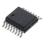
♦ Small 16-Pin QSOP and 16-Pin TSSOP Packages
♦ 2-Wire SMBus Interface
Ordering Information
The MAX6698 is specified for an operating temperature
range of -40°C to +125°C and is available in 16-pin
QSOP and 16-pin TSSOP packages.
Applications
Desktop Computers
Workstations
Notebook Computers
Servers
PINPACKAGE
PKG
CODE
-40°C to +125°C
16 QSOP
E16-1
-40°C to +125°C
16 TSSOP
U16-1
PART
TEMP RANGE
MAX6698EE_ _
MAX6698UE_ _
*See the Slave Address section.
Pin Configuration appears at end of data sheet.
Typical Application Circuit
+3.3V
1
DXP1
GND 16
2
DXN1
3
DXP2
SMBDATA 14
4
DXN2
ALERT 13
5
DXP3
VCC 12
6
DXN3
OVERT 11
7
THER3
THER1 10
8
VREF
THER2
MAX6698
SMBCLK 15
9
REX3
REX2
RTHER3
RTHER2
REX1
RTHER1
SMBus is a trademark of Intel Corp.
________________________________________________________________ Maxim Integrated Products
For pricing, delivery, and ordering information, please contact Maxim Direct at 1-888-629-4642,
or visit Maxim’s website at www.maxim-ic.com.
1
MAX6698
General Description
�MAX6698
7-Channel Precision Remote-Diode, Thermistor,
and Local Temperature Monitor
ABSOLUTE MAXIMUM RATINGS
VCC, SCL, SDA, ALERT, OVERT to GND ................-0.3V to +6V
DXP_ to GND..............................................-0.3V to (VCC + 0.3V)
DXN_ to GND ........................................................-0.3V to +0.8V
THER_ to GND..........................................................-0.3V to +6V
VREF to GND............................................................-0.3V to +6V
SDA, ALERT, OVERT Current .............................-1mA to +50mA
DXN Current .......................................................................±1mA
Continuous Power Dissipation (TA = +70°C)
16-Pin QSOP
(derate 8.3mW/°C above +70°C) ......................666.7mW(E16-1)
16-Pin TSSOP
(derate 9.4mW/°C above +70°C)....................754.7mW(U16-1)
ESD Protection (all pins, Human Body Model) ................±2000V
Operating Temperature Range .........................-40°C to +125°C
Junction Temperature ......................................................+150°C
Storage Temperature Range .............................-60°C to +150°C
Lead Temperature (soldering, 10s) .................................+300°C
Stresses beyond those listed under “Absolute Maximum Ratings” may cause permanent damage to the device. These are stress ratings only, and functional
operation of the device at these or any other conditions beyond those indicated in the operational sections of the specifications is not implied. Exposure to
absolute maximum rating conditions for extended periods may affect device reliability.
ELECTRICAL CHARACTERISTICS
(VCC = +3.0V to +5.5V, TA = -40°C to +125°C, unless otherwise noted. Typical values are at VCC = +3.3V and TA = +25°C.) (Note 1)
PARAMETER
Supply Voltage
SYMBOL
CONDITIONS
VCC
MIN
TYP
3.0
Standby Supply Current
ISS
SMBus static
30
Operating Current
ICC
During conversion
500
Channel 1 only
11
Other diode channels
8
Temperature Resolution
Remote Temperature Accuracy
VCC = 3.3V
Local Temperature Accuracy
VCC = 3.3V
UNITS
5.5
V
1000
µA
µA
Bits
TA = TRJ = +60°C to +100°C
-1.0
+1.0
TA = TRJ = 0°C to +125°C
-3.0
+3.0
DXN_ grounded,
TRJ = TA = 0°C to +85°C
TA = +60°C to +100°C
-2.5
+2.5
TA = 0°C to +125°C
-3.5
+3.5
o
±0.2
Remote Channel 1 Conversion
Time
tCONV1
Remote Channels 2 Through 6
Conversion Time
tCONV_
Remote-Diode Source Current
IRJ
UVLO
Resistance cancellation on
95
125
156
Resistance cancellation off
190
250
312
95
125
156
High level
80
100
120
Low level
8
10
12
2.3
2.80
2.95
Falling edge of VCC disables ADC
Undervoltage-Lockout Hysteresis
90
Power-On Reset (POR) Threshold
VCC falling edge
o
C
o
C
±2.5
Supply Sensitivity of Temperature
Accuracy
Undervoltage-Lockout Threshold
MAX
1.2
POR Threshold Hysteresis
2.0
C/V
ms
ms
µA
V
mV
2.5
90
V
mV
THERMISTOR CONVERSION
Voltage-Measurement Accuracy
-1
Conversion Time
Thermistor Reference Voltage
2
VREF
+1
%Full
scale
31
ms
1
V
_______________________________________________________________________________________
�7-Channel Precision Remote-Diode, Thermistor,
and Local Temperature Monitor
(VCC = +3.0V to +5.5V, TA = -40°C to +125°C, unless otherwise noted. Typical values are at VCC = +3.3V and TA = +25°C.) (Note 1)
PARAMETER
SYMBOL
Reference-Load Regulation
CONDITIONS
MIN
TYP
0mA < IREF < 2mA
Reference-Supply Rejection
MAX
UNITS
0.4
%
0.5
%/V
ALERT, OVERT
Output Low Voltage
VOL
ISINK = 1mA
0.3
ISINK = 6mA
0.5
Output Leakage Current
V
1
µA
0.8
V
SMBus INTERFACE (SCL, SDA)
Logic-Input Low Voltage
Logic-Input High Voltage
VIL
VIH
VCC = 3.0V
2.2
V
VCC = 5.0V
2.4
V
Input Leakage Current
-1
Output Low Voltage
VOL
Input Capacitance
CIN
+1
ISINK = 6mA
0.3
5
µA
V
pF
SMBus-COMPATIBLE TIMING (Figures 3 and 4) (Note 2)
Serial Clock Frequency
Bus Free Time Between STOP
and START Condition
fSCL
tBUF
START Condition Setup Time
Repeat START Condition Setup
Time
tSU:STA
START Condition Hold Time
tHD:STA
STOP Condition Setup Time
tSU:STO
Clock Low Period
tLOW
Clock High Period
tHIGH
Data Hold Time
tHD:DAT
Data Setup Time
tSU:DAT
Receive SCL/SDA Rise Time
Receive SCL/SDA Fall Time
Pulse Width of Spike Suppressed
SMBus Timeout
Note 1:
Note 2:
Note 3:
Note 4:
tR
(Note 3)
400
fSCL = 100kHz
4.7
fSCL = 400kHz
1.6
fSCL = 100kHz
4.7
fSCL = 400kHz
0.6
90% of SCL to 90% of SDA, fSCL = 100kHz
0.6
90% of SCL to 90% of SDA, fSCL = 400kHz
0.6
10% of SDA to 90% of SCL
0.6
90% of SCL to 90% of SDA, fSCL = 100kHz
4
90% of SCL to 90% of SDA, fSCL = 400kHz
0.6
10% to 10%, fSCL = 100kHz
1.3
10% to 10%, fSCL = 400kHz
1.3
90% to 90%
0.6
fSCL = 100kHz
300
µs
µs
µs
µs
µs
µs
µs
fSCL = 400kHz (Note 4)
900
fSCL = 100kHz
250
fSCL = 400kHz
100
1
fSCL = 400kHz
0.3
tF
tTIMEOUT
300
0
SDA low period for interface reset
25
ns
ns
fSCL = 100kHz
tSP
kHz
37
µs
ns
50
ns
45
ms
All parameters are tested at TA = +25°C. Specifications over temperature are guaranteed by design.
Timing specifications are guaranteed by design.
The serial interface resets when SCL is low for more than tTIMEOUT.
A transition must internally provide at least a hold time to bridge the undefined region (300ns max) of SCL’s falling edge.
_______________________________________________________________________________________
3
MAX6698
ELECTRICAL CHARACTERISTICS (continued)
�Typical Operating Characteristics
(VCC = 3.3V, TA = +25°C, unless otherwise noted.)
350
345
340
335
330
3
2
1
0
0
-1
-2
-3
325
-4
320
4.8
3.3
5.3
3.8
2
1
0
-1
-2
-3
-4
100mVP-P
3
2
1
0
-1
-2
50
75
100
1
0
-1
-2
-5
0.001
0.01
0.1
FREQUENCY (MHz)
REMOTE TEMPERATURE ERROR
vs. COMMON-MODE NOISE FREQUENCY
MAX6698 toc07
5
4
TEMPERATURE ERROR (°C)
TEMPERATURE ERROR (°C)
100mVP-P
FREQUENCY (MHz)
3
2
1
0
-1
-2
-3
100mVP-P
3
2
1
0
-1
-2
-3
-4
-4
-5
0.001
-5
0.001
0.01
0.1
FREQUENCY (MHz)
1
10
125
1
-4
0.1
100mVP-P
100
2
-4
125
75
3
-3
REMOTE TEMPERATURE ERROR
vs. COMMON-MODE NOISE FREQUENCY
4
4
-3
DIE TEMPERATURE (°C)
5
5
MAX6698 toc08
25
50
LOCAL TEMPERATURE ERROR
vs. POWER-SUPPLY NOISE FREQUENCY
-5
0
25
REMOTE-DIODE TEMPERATURE ERROR
vs. POWER-SUPPLY NOISE FREQUENCY
4
TEMPERATURE ERROR (°C)
3
0
REMOTE-DIODE TEMPERATURE (°C)
5
MAX6698 toc04
4
5.3
SUPPLY VOLTAGE (V)
SUPPLY VOLTAGE (V)
LOCAL TEMPERATURE ERROR
vs. DIE TEMPERATURE
4.8
4.3
TEMPERATURE ERROR (°C)
4.3
MAX6698 toc05
3.8
MAX6698 toc03
1
MAX6698 toc06
7
6
5
4
2
TEMPERATURE ERROR (°C)
SUPPLY CURRENT (µA)
355
8
3
MAX6698 toc02
360
MAX6698 toc01
STANDBY SUPPLY CURRENT (µA)
12
11
10
9
3.3
4
REMOTE TEMPERATURE ERROR
vs. REMOTE-DIODE TEMPERATURE
SUPPLY CURRENT
vs. SUPPLY VOLTAGE
STANDBY SUPPLY CURRENT
vs. SUPPLY VOLTAGE
TEMPERATURE ERROR (°C)
MAX6698
7-Channel Precision Remote-Diode, Thermistor,
and Local Temperature Monitor
0.01
0.1
1
10
FREQUENCY (MHz)
_______________________________________________________________________________________
1
�7-Channel Precision Remote-Diode, Thermistor,
and Local Temperature Monitor
-1.5
-2.0
-2.5
-3.0
-3.5
-4.0
VOL = 0.3V
25
20
15
VOL = 0.1V
10
MAX6698 toc11
MAX6698 toc10
-1.0
5
100mVP-P
4
TEMPERATURE ERROR (°C)
TEMPERATURE ERROR (°C)
-0.5
30
ALERT SINK CURRENT (mA)
MAX6698 toc09
0
THERMISTOR ADC ERROR
vs. POWER-SUPPLY NOISE FREQUENCY
ALERT, OVERT SINK CURRENT
vs. TEMPERATURE
TEMPERATURE ERROR
vs. DXP-DXN CAPACITANCE
3
2
1
0
-1
-2
-3
5
-4
-4.5
-5
0
-5.0
1
100
10
DXP-DXN CAPACITANCE (nF)
0
25
50
75
100
125
0.01
0.1
1
10
100
FREQUENCY (MHz)
TEMPERATURE (°C)
Pin Description
PIN
NAME
FUNCTION
1
DXP1
Combined Current Source and A/D Positive Input for Channel 1 Remote Diode. Connect to the anode
of a remote-diode-connected temperature-sensing transistor. Leave floating or connect to VCC if no
remote diode is used. Place a 2200pF capacitor between DXP1 and DXN1 for noise filtering.
2
DXN1
Cathode Input for Channel 1 Remote Diode. Connect the cathode of the channel 1 remote-diodeconnected transistor to DXN1.
3
DXP2
Combined Current Source and A/D Positive Input for Channel 2 Remote Diode. Connect to the anode
of a remote-diode-connected temperature-sensing transistor. Leave floating or connect to VCC if no
remote diode is used. Place a 2200pF capacitor between DXP2 and DXN2 for noise filtering.
4
DXN2
Cathode Input for Channel 2 Remote Diode. Connect the cathode of the channel 2 remote-diodeconnected transistor to DXN2.
5
DXP3
Combined Current Source and A/D Positive Input for Channel 3 Remote Diode. Connect to the anode
of a remote-diode-connected temperature-sensing transistor. Leave floating or connect to VCC if no
remote diode is used. Place a 2200pF capacitor between DXP3 and DXN3 for noise filtering.
6
DXN3
Cathode Input for Channel 3 Remote Diode. Connect the cathode of the channel 1 remote-diodeconnected transistor to DXN3.
7
THER3
Thermistor Voltage Sense Input 3. Connect thermistor 3 between THER3 and ground and an external
resistor REXT3 between THER3 and VREF.
8
VREF
Thermistor Reference Voltage (1V Nominal). VREF is automatically enabled for a thermistor
conversion, and is disabled for diode measurements.
_______________________________________________________________________________________
5
MAX6698
Typical Operating Characteristics (continued)
(VCC = 3.3V, TA = +25°C, unless otherwise noted.)
�7-Channel Precision Remote-Diode, Thermistor,
and Local Temperature Monitor
MAX6698
Pin Description (continued)
PIN
NAME
FUNCTION
9
THER2
Thermistor Voltage Sense Input 2. Connect thermistor 2 between THER2 and ground and an external
resistor REXT3 between THER2 and VREF.
10
THER1
Thermistor Voltage Sense Input 1. Connect thermistor 1 between THER1 and ground and an external
resistor REXT3 between THER1 and VREF.
11
OVERT
Overtemperature Active-Low, Open-Drain Output. OVERT asserts low when the temperature of
channels 1, 4, 5, and 6 exceed the programmed threshold limit.
12
VCC
13
ALERT
14
SMBDATA
15
SMBCLK
16
GND
Supply Voltage Input. Bypass to GND with a 0.1µF capacitor.
SMBus Alert (Interrupt), Active-Low, Open-Drain Output. ALERT asserts low when the temperature of
channels 1, 4, 5, and 6 exceed programmed threshold limit.
SMBus Serial-Data Input/Output. Connect to a pullup resistor.
SMBus Serial-Clock Input. Connect to a pullup resistor.
Ground
Detailed Description
The MAX6698 is a precision multichannel temperature
monitor that features one local, three remote thermal
diode temperature-sensing channels, and three thermistor voltage-sensing channels. All channels have a
programmable alert threshold for each temperature
channel and a programmable overtemperature threshold for channels 1, 4, 5, and 6 (see Figure 1).
Communication with the MAX6698 is achieved through
the SMBus serial interface and a dedicated alert
(ALERT) pin. The alarm outputs, OVERT and ALERT,
assert if the software-programmed temperature thresholds are exceeded. ALERT typically serves as an interrupt, while OVERT can be connected to a fan, system
shutdown, or other thermal-management circuitry.
Note that thermistor “temperature data” is really the voltage across the fixed resistor, REXT, in series with the
thermistor. This voltage is directly related to temperature,
but the data is expressed in percentage of the reference
voltage not in °C.
ADC Conversion Sequence
In the default conversion mode, the MAX6698 starts the
conversion sequence by measuring the temperature on
the channel 1 remote diode, followed by the channel 2,
remote diode, channel 3 remote diode, and the local
channel. Then it measures thermistor channel 1, thermistor channel 2, and thermistor channel 3. The con-
6
version result for each active channel is stored in the
corresponding temperature data register.
In some systems, one of the remote thermal diodes may
be monitoring a location that experiences temperature
changes that occur much more rapidly than in the other
channels. If faster temperature changes must be monitored in one of the temperature channels, the MAX6698
allows channel 1 to be monitored at a faster rate than the
other channels. In this mode (set by writing a 1 to bit 4 of
the configuration 1 register), measurements of channel 1
alternate with measurements of the other channels. The
sequence becomes remote-diode channel 1, remotediode channel 2, remote-diode channel 1, remote-diode
channel 3, remote-diode channel 1, etc. Note that the
time required to measure all seven channels is considerably greater in this mode than in the default mode.
Low-Power Standby Mode
Standby mode reduces the supply current to less than
15µA by disabling the internal ADC. Enter standby by
setting the STOP bit to 1 in the configuration 1 register.
During standby, data is retained in memory, and the
SMBus interface is active and listening for SMBus commands. The timeout is enabled if a start condition is recognized on the SMBus. Activity on the SMBus causes
the supply current to increase. If a standby command is
received while a conversion is in progress, the conversion cycle is interrupted, and the temperature registers
are not updated. The previous data is not changed and
remains available.
_______________________________________________________________________________________
�7-Channel Precision Remote-Diode, Thermistor,
and Local Temperature Monitor
10/100µA
DXP1
OVERT
MAX6698
DXN1
3-TO-1
MUX
DXP3
INPUT
BUFFER
ALU
DP
ALERT
DXN3
BUF1
VREF
ADC
CNT
COMMAND BYTE
COUNTER
VREF1
REGISTER BANK
REMOTE TEMPERATURES
LOCAL TEMPERATURES
REXT1
ALERT THRESHOLD
OVERT THRESHOLD
RTHER1
ALERT RESPONSE ADDRESS
SMBus
INTERFACE
REXT2
3-TO-1
MUX
BUF2
RTHER1
REXT1
RTHER1
SCL
SDA
Figure 1. Internal Block Diagram
SMBus Digital Interface
From a software perspective, the MAX6698 appears as
a series of 8-bit registers that contain temperature measurement data, alarm threshold values, and control bits.
A standard SMBus-compatible 2-wire serial interface is
used to read temperature data and write control bits
and alarm threshold data. The same SMBus slave
address also provides access to all functions.
The MAX6698 employs four standard SMBus protocols:
write byte, read byte, send byte, and receive byte
(Figure 2). The shorter receive byte protocol allows
quicker transfers, provided that the correct data regis-
ter was previously selected by a read byte instruction.
Use caution with the shorter protocols in multimaster
systems, since a second master could overwrite the
command byte without informing the first master. Figure
3 is the SMBus write timing diagram and Figure 4 is the
SMBus read timing diagram.
The remote diode 1 measurement channel provides 11
bits of data (1 LSB = 0.125°C). All other temperaturemeasurement channels provide 8 bits of temperature
data (1 LSB = 1°C). The 8 most significant bits (MSBs)
can be read from the local temperature, remote temperature, and thermistor registers. The remaining 3 bits
_______________________________________________________________________________________
7
MAX6698
VCC
�MAX6698
7-Channel Precision Remote-Diode, Thermistor,
and Local Temperature Monitor
Write Byte Format
S
ADDRESS
WR
ACK
COMMAND
7 bits
ACK
DATA
8 bits
Slave Address: equivalent to chip-select line of
a 3-wire interface
ACK
P
8 bits
Command Byte: selects which
register you are writing to
1
Data Byte: data goes into the register
set by the command byte (to set
thresholds, configuration masks, and
sampling rate)
Read Byte Format
S
ADDRESS
WR
ACK
7 bits
COMMAND
ACK
ACK
DATA
///
P
8 bits
Slave Address: repeated
due to change in dataflow direction
Data Byte: reads from
the register set by the
command byte
Receive Byte Format
WR
7 bits
ACK
COMMAND
ACK
P
8 bits
S
ADDRESS
7 bits
RD
ACK
DATA
///
P
8 bits
Data Byte: reads data from
the register commanded
by the last read byte or
write byte transmission;
also used for SMBus alert
response return address
Command Byte: sends command with no data, usually
used for one-shot command
S = Start condition
P = Stop condition
RD
7 bits
Command Byte: selects
which register you are
reading from
Send Byte Format
ADDRESS
ADDRESS
8 bits
Slave Address: equivalent to chip-select line
S
S
Shaded = Slave transmission
/// = Not acknowledged
Figure 2. SMBus Protocols
for remote diode 1 can be read from the extended temperature register. If extended resolution is desired, the
extended resolution register should be read first. This
prevents the most significant bits from being overwritten
by new conversion results until they have been read. If
the most significant bits have not been read within an
SMBus timeout period (nominally 25ms), normal updating continues. Table 1 shows themistor voltage data format. Table 2 shows the main temperature register (high
byte) data format. Table 3 shows the extended resolution temperature register (low byte) data format.
Diode Fault Detection
If a channel’s input DXP_ and DXN_ are left open, the
MAX6698 detects a diode fault. An open diode fault
does not cause either ALERT or OVERT to assert. A bit
in the status register for the corresponding channel is
set to 1 and the temperature data for the channel is
stored as all 1s (FFh). It takes approximately 4ms for
the MAX6698 to detect a diode fault. Once a diode fault
is detected, the MAX6698 goes to the next channel in
the conversion sequence. Depending on operating
conditions, a shorted diode may or may not cause
ALERT or OVERT to assert, so if a channel will not be
used, disconnect its DXP and DXN inputs.
8
Table 1. Thermistor Voltage Data Format
VREXT
DIGITAL OUTPUT
1.000
1100 1000
0.500
0110 0100
0.250
0011 0010
0.055
0000 1011
0.050
0000 1010
0.005
0000 0001
0.000
0000 0000
Alarm Threshold Registers
There are 11 alarm threshold registers that store overtemperature ALERT and OVERT threshold values.
Seven of these registers are dedicated to store one
local alert temperature threshold limit, three remote alert
temperature threshold limits, and three thermistor voltage threshold limits (see the ALERT Interrupt Mode section). The remaining four registers are dedicated to
remote-diode channel 1, and three thermistor channels
1, 2, and 3 to store overtemperature threshold limits
(see the OVERT Overtemperature Alarm section).
Access to these registers is provided through the
SMBus interface.
_______________________________________________________________________________________
�7-Channel Precision Remote-Diode, Thermistor,
and Local Temperature Monitor
B
tLOW
C
D
E
F
G
H
tHIGH
I
J
K
L
MAX6698
A
M
SMBCLK
SMBDATA
tSU:STA tHD:STA
tSU:STO
tSU:DAT
A = START CONDITION
B = MSB OF ADDRESS CLOCKED INTO SLAVE
C = LSB OF ADDRESS CLOCKED INTO SLAVE
D = R/W BIT CLOCKED INTO SLAVE
E = SLAVE PULLS SMBDATA LINE LOW
F = ACKNOWLEDGE BIT CLOCKED INTO MASTER
G = MSB OF DATA CLOCKED INTO SLAVE
H = LSB OF DATA CLOCKED INTO SLAVE
tBUF
I = MASTER PULLS DATA LINE LOW
J = ACKNOWLEDGE CLOCKED INTO SLAVE
K = ACKNOWLEDGE CLOCK PULSE
L = STOP CONDITION
M = NEW START CONDITION
Figure 3. SMBus Write Timing Diagram
A
tLOW
B
C
tHIGH
D
E
F
G
H
I
J
K
L
M
SMBCLK
SMBDATA
tSU:STA
tHD:STA
tSU:DAT
A = START CONDITION
B = MSB OF ADDRESS CLOCKED INTO SLAVE
C = LSB OF ADDRESS CLOCKED INTO SLAVE
D = R/W BIT CLOCKED INTO SLAVE
E = SLAVE PULLS SMBDATA LINE LOW
tHD:DAT
tSU:STO tBUF
J = ACKNOWLEDGE CLOCKED INTO SLAVE
K = ACKNOWLEDGE CLOCK PULSE
L = STOP CONDITION
M = NEW START CONDITION
F = ACKNOWLEDGE BIT CLOCKED INTO MASTER
G = MSB OF DATA CLOCKED INTO MASTER
H = LSB OF DATA CLOCKED INTO MASTER
I = MASTER PULLS DATA LINE LOW
Figure 4. SMBus Read Timing Diagram
Table 2. Main Temperature Register (High
Byte) Data Format
TEMP (°C)
DIGITAL OUTPUT
>127
0111 1111
127
0111 1111
126
0111 1110
25
00011001
0.00
0000 0000