19-2531; Rev 2; 12/05
Low-Power Dual-/Triple-Voltage SC70 µP
Supervisory Circuits
The MAX6736–MAX6745 are low-power dual-/triplevoltage microprocessor (µP) supervisors. These
devices assert a reset if any monitored supply falls
below its factory-trimmed or adjustable threshold and
maintain reset for a minimum timeout period after all
supplies rise above their thresholds. The integrated
dual/triple supervisory circuits significantly reduce size
and power compared to separate ICs or discrete components. The low supply current of 6µA makes these
devices ideal for portable equipment.
The MAX6736/MAX6737 are dual fixed-voltage µP
supervisors with a manual reset input. The MAX6738/
MAX6739 have one fixed and one adjustable reset
threshold and a manual reset input. The MAX6740/
MAX6743 are triple-voltage µP supervisors with two
fixed and one user-adjustable reset threshold inputs.
The MAX6741/MAX6744 are dual-voltage µP supervisors with a power-OK (POK) output ideal for powersupply sequencing. The MAX6742/MAX6745 monitor
the primary V CC supply and have an independent
power-fail comparator.
The MAX6736–MAX6745 monitor I/O supply voltages
(V CC1) from 1.8V to 5.0V and core supply voltages
(VCC2) from 0.9V to 3.3V with factory-trimmed reset
threshold voltage options (Table 1). An external
adjustable RSTIN input option allows monitoring voltages down to 0.5V.
Features
♦ Dual-/Triple-Supply Reset Voltage Monitors
♦ Precision Factory-Set Reset Thresholds for
Monitoring from 0.9V to 5.0V
♦ Adjustable Reset Input Down to 0.488V
♦ 150ms and 1200ms (min) Reset Timeout Period
Options
♦ VCC1 Power-OK Output for Power-Supply
Sequencing Applications (MAX6741/MAX6744)
♦ Power-Fail Input/Power-Fail Output
(MAX6742/MAX6745)
♦ 6µA Supply Current
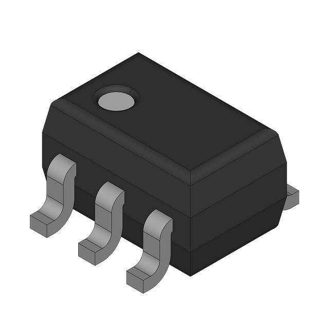
♦ Tiny SC70 Package
A variety of push-pull or open-drain reset outputs along
with manual reset input and power-fail input/output features are available (see the Selector Guide). The
MAX6736–MAX6745 are offered in a space-saving 5-pin
SC70 package and operate over the -40°C to +85°C
temperature range.
Applications
Portable/BatteryPowered Equipment
Controllers
Multivoltage Systems
GPS Equipment
Notebook Computers
POS Equipment
PDAs
Ordering Information
PART
TEMP RANGE
PIN-PACKAGE
MAX6736XK_ _D_-T
-40°C to +85°C
5 SC70-5
MAX6737XK_ _D_-T
-40°C to +85°C
5 SC70-5
Note: The first “_ _” or “_” are placeholders for the threshold
voltage levels of the devices. Desired threshold levels are set
by the part number suffix found in Tables 1 and 2. The “_” after
the D is a placeholder for the reset timeout period suffix found
in Table 3. For example, the MAX6736XKLTD3-T is a dual-voltage supervisor VTH1 = 4.625V, VTH2 = 3.075V, and a 150ms
minimum reset timeout period. All devices are available in
tape-and-reel only. There is a 2500-piece minimum order
increment for standard versions (see Table 1). Sample stock is
typically held on standard versions only. Nonstandard versions
require a minimum order increment of 10,000 pieces. Contact
factory for availability.
Devices are available in both leaded and lead-free packaging.
Specify lead-free by replacing “-T” with “+T” when ordering.
Ordering Information and Selector Guide continued at end
of data sheet.
Pin Configurations, Typical Application Circuits, and
Functional Diagram appear at end of data sheet.
Selector Guide
PART
VOLTAGE
MONITORS
MAX6736
MAX6737
MAX6738
POWER-FAIL
INPUT/
OUTPUT
OPEN-DRAIN
RESET
PUSH-PULL
RESET
2 fixed
X
—
X
—
—
—
2 fixed
—
X
X
—
—
—
1 fixed, 1 adj
X
—
X
—
—
X
MANUAL
RESET
POK
OUTPUT
RSTIN
INPUT
*Manual reset detect on RESET output.
________________________________________________________________ Maxim Integrated Products
For pricing, delivery, and ordering information, please contact Maxim/Dallas Direct! at
1-888-629-4642, or visit Maxim’s website at www.maxim-ic.com.
1
MAX6736–MAX6745
General Description
�MAX6736–MAX6745
Low-Power Dual-/Triple-Voltage SC70 µP
Supervisory Circuits
ABSOLUTE MAXIMUM RATINGS
VCC1, VCC2, POK1 to GND ......................................-0.3V to +6V
Open-Drain RESET, PFO to GND.............................-0.3V to +6V
Push-Pull RESET to GND..........................-0.3V to (VCC1 + 0.3V)
MR, RSTIN, PFI to GND............................-0.3V to (VCC1 + 0.3V)
Input/Output Current, All Pins .............................................20mA
Continuous Power Dissipation (TA = +70°C)
5-Pin SC70 (derate 3.1mW/°C above +70°C) ..............247mW
Operating Temperature Range ...........................-40°C to +85°C
Junction Temperature ......................................................+150°C
Storage Temperature Range .............................-65°C to +150°C
Lead Temperature (soldering, 10s) .................................+300°C
Stresses beyond those listed under “Absolute Maximum Ratings” may cause permanent damage to the device. These are stress ratings only, and functional
operation of the device at these or any other conditions beyond those indicated in the operational sections of the specifications is not implied. Exposure to
absolute maximum rating conditions for extended periods may affect device reliability.
ELECTRICAL CHARACTERISTICS
(VCC = 1.2V to 5.5V, TA = -40°C to +85°C, unless otherwise noted. Typical values are at TA = +25°C.) (Note 1)
PARAMETER
Operating Voltage Range
VCC1 Supply Current
VCC2 Supply Current
SYMBOL
VCC1,
VCC2
ICC1
ICC2
CONDITIONS
TA = 0°C to +85°C
1.0
5.5
VCC1 = 3.3V, VCC1 > VCC2, no load, reset
not asserted
5
10
VCC1 = 1.8V, VCC1 < VCC2, no load, reset
not asserted
5
10
VCC2 = 1.8V, VCC2 < VCC1, no load, reset
not asserted
1
2
VCC2 = 3.3V, VCC2 > VCC1, no load, reset
not asserted
10
20
UNITS
V
µA
µA
MAX67_ _T
MAX67_ _S
MAX67_ _R
MAX67_ _Z
MAX67_ _Y
MAX67_ _W
MAX67_ _V
2
MAX
5.5
MAX67_ _M
VTH1
TYP
1.2
MAX67_ _L
Reset Threshold for VCC1
MIN
TA = -40°C to 0°C
TA = 0°C to +85°C
4.500
TA = -40°C to +85°C
4.425
TA = 0°C to +85°C
4.250
TA = -40°C to +85°C
4.175
TA = 0°C to +85°C
3.000
TA = -40°C to +85°C
2.950
TA = 0°C to +85°C
2.850
TA = -40°C to +85°C
2.800
TA = 0°C to +85°C
2.550
TA = -40°C to +85°C
2.505
TA = 0°C to +85°C
2.250
TA = -40°C to +85°C
2.213
TA = 0°C to +85°C
2.125
TA = -40°C to +85°C
2.088
TA = 0°C to +85°C
1.620
TA = -40°C to +85°C
1.593
TA = 0°C to +85°C
1.530
TA = -40°C to +85°C
1.503
4.625
4.750
4.825
4.375
4.500
4.575
3.075
3.150
3.200
2.925
3.000
3.050
2.625
2.700
2.745
2.313
2.375
2.413
2.188
2.250
2.288
1.665
1.710
1.737
1.575
_______________________________________________________________________________________
1.620
1.647
V
�Low-Power Dual-/Triple-Voltage SC70 µP
Supervisory Circuits
(VCC = 1.2V to 5.5V, TA = -40°C to +85°C, unless otherwise noted. Typical values are at TA = +25°C.) (Note 1)
PARAMETER
SYMBOL
CONDITIONS
MAX67_ _T
MAX67_ _S
MAX67_ _R
MAX67_ _Z
MAX67_ _Y
MAX67_ _W
Reset Threshold for VCC2
VTH2
MAX67_ _V
MAX67_ _I
MAX67_ _H
MAX67_ _G
MAX67_ _F
MAX67_ _E
MAX67_ _D
RSTIN Threshold (MAX6738/
MAX6739/MAX6740/MAX6743)
VTH-RSTIN
MIN
TYP
MAX
TA = 0°C to +85°C
3.000
3.075
3.150
TA = -40°C to +85°C
2.905
TA = 0°C to +85°C
2.850
TA = -40°C to +85°C
2.800
TA = 0°C to +85°C
2.550
TA = -40°C to +85°C
2.505
TA = 0°C to +85°C
2.250
TA = -40°C to +85°C
2.213
TA = 0°C to +85°C
2.125
TA = -40°C to +85°C
2.088
TA = 0°C to +85°C
1.620
TA = -40°C to +85°C
1.593
TA = 0°C to +85°C
1.530
TA = -40°C to +85°C
1.503
TA = 0°C to +85°C
1.350
TA = -40°C to +85°C
1.328
TA = 0°C to +85°C
1.275
TA = -40°C to +85°C
1.253
TA = 0°C to +85°C
1.080
TA = -40°C to +85°C
1.062
TA = 0°C to +85°C
1.020
TA = -40°C to +85°C
1.002
TA = 0°C to +85°C
0.810
TA = -40°C to +85°C
0.797
TA = 0°C to + 85°C
0.765
TA = -40°C to +85°C
0.752
TA = 0°C to +85°C
0.476
TA = -40°C to +85°C
0.468
RSTIN Input Current
VRSTIN ≥ 0.1V (Note 2)
Reset Threshold Hysteresis
VTH1, VTH2, RSTIN, PFI
RESET, POK1 Output Low
RESET Output High (Push-Pull)
VOL
VOH
3.050
2.925
3.000
3.050
2.625
2.700
2.745
2.313
2.375
2.413
2.188
2.250
2.288
1.665
1.710
1.737
1.575
1.620
1.647
1.388
1.425
1.350
1.373
1.110
1.140
1.158
1.050
1.080
1.098
0.833
0.855
0.869
0.788
0.810
0.824
0.488
0.500
0.507
+10
0.5
0.3
VCC1 ≥ 1.2V, ISINK = 100µA
0.3
VCC1 ≥ 2.13V, ISINK = 1.2mA
0.3
VCC1 ≥ 4.25V, ISINK = 3.2mA,
0.4
VCC1 ≥ 4.75V, ISOURCE = 800µA, output
deasserted
0.8 ×
VCC
V
nA
%
VCC1 ≥ 1.0V, ISINK = 50µA, TA = 0°C to
+85°C
0.8 ×
VCC
V
1.448
1.313
-10
VCC1 ≥ 2.38V, ISOURCE = 500µA, output
deasserted
UNITS
V
V
_______________________________________________________________________________________
3
MAX6736–MAX6745
ELECTRICAL CHARACTERISTICS (continued)
�MAX6736–MAX6745
Low-Power Dual-/Triple-Voltage SC70 µP
Supervisory Circuits
ELECTRICAL CHARACTERISTICS (continued)
(VCC = 1.2V to 5.5V, TA = -40°C to +85°C, unless otherwise noted. Typical values are at TA = +25°C.) (Note 1)
PARAMETER
RESET Output Open-Drain
Leakage Current
(MAX6736/MAX6738)
SYMBOL
ILKG
POK1 Output Open-Drain
Leakage
VCC Reset Delay
tRD
VCC Reset Timeout Period
(Note 3)
tRP
CONDITIONS
MIN
MAX
UNITS
Output not asserted low (Note 2)
500
nA
Output not asserted low (Note 2)
500
nA
VCC1, VCC2, or RSTIN falling at 10mV/µs
from VTH + 100mV to VTH - 100mV
TYP
35
µs
MAX67_ _ _ _ XK_ _D3
150
225
300
MAX67_ _ _ _ XK_ _ D7
1200
1800
2400
0.75
1.5
3.00
kΩ
150
225
300
ms
ms
MANUAL RESET (MAX6736–MAX6739 only)
MR to VCC1 Internal Pullup
Impedance
MR Timeout Period
tMRP
MR Minimum Input Pulse Width
tMPW
Both D3 and D7 timing options
1
MR Glitch Rejection
µs
100
ns
0.3 ×
VCC1
VIL
MR Input Voltage
0.8 ×
VCC1
VIH
MR to RESET Delay
300
V
ns
VCC1 POWER-OK OUTPUT (MAX6741/MAX6744 only)
POK1 Timeout Period
tPOKP
37.5
56.25
75.0
ms
25
50
100
kΩ
37.5
56.25
75.0
ms
PUSHBUTTON RESET (MAX6740/MAX6741/MAX6742 only)
RESET to VCC1 Internal Pullup
Impedance
Manual Reset Detect Debounce
Period
tDEB
Manual Reset Timeout
Period (Note 3)
tMRP
Manual Reset Minimum Input
Pulse Width
tMPW
(Note 4)
MAX67_ _ _ _ XK_ _D3
150
225
300
MAX67_ _ _ _ XK_ _ D7
1200
1800
2400
(Note 4)
1
ms
µs
Manual Reset Release Detect
Threshold
(Note 4)
0.5 ×
VCC1
V
Manual Reset Glitch Rejection
(Note 4)
100
ns
300
ns
Manual Reset to RESET Delay
4
_______________________________________________________________________________________
�Low-Power Dual-/Triple-Voltage SC70 µP
Supervisory Circuits
(VCC = 1.2V to 5.5V, TA = -40°C to +85°C, unless otherwise noted. Typical values are at TA = +25°C.) (Note 1)
PARAMETER
SYMBOL
CONDITIONS
MIN
TYP
MAX
TA = 0°C to +85°C
0.476
0.488
TA = -40°C to +85°C
0.468
0.507
VPFI ≥ 0.1V (Note 2)
-10
+10
UNITS
POWER-FAIL COMPARATOR (MAX6742/MAX6745 only)
Power Fail In Threshold (Note 5)
VTH-PFI
Power Fail In Current
IPFI
PFO Output Low
VOL
PFI to PFO Propagation Delay
tP
PFO Startup Delay
0.500
VCC1 ≥ 1.53V, ISINK = 500µA
0.3
VCC1 ≥ 2.03V, ISINK = 1.2mA
0.3
VCC1 ≥ 4.25V, ISINK = 3.2mA
0.4
V
nA
V
PFI falling at 10mV/µs from VTH-PFI +
100mV to VTH-PFI - 100mV or rising at
10mV/µs from VTH-PFI - 100mV to VTH-PFI +
100mV (Note 5)
35
µs
To output valid (Note 5)
5
ms
All devices are 100% tested at TA = +25°C. All temperature limits are guaranteed by design.
Guaranteed by design.
tRD timeout period begins after POK1 timeout period (tPOKP) and VCC2 ≥ VTH2 (max) (MAX6741/MAX6744).
Refers to the manual reset function obtained by forcing the RESET output low.
VCC1 ≥ 1.6V.
Note 1:
Note 2:
Note 3:
Note 4:
Note 5:
Typical Operating Characteristics
(TA = +25°C, unless otherwise noted.)
TOTAL
6
ICC1
5
4
3
2
8
7
6
TOTAL
5
ICC1
4
3
2
ICC2
1
0
-20
0
20
40
TEMPERATURE (°C)
60
80
8
7
6
TOTAL
5
4
ICC1
3
ICC2
1
0
-40
VCC1 = 1.8V, VCC2 = 1.2V
9
2
ICC2
1
10
SUPPLY CURRENT (µA)
7
SUPPLY CURRENT (µA)
SUPPLY CURRENT (µA)
8
VCC1 = 2.5V, VCC2 = 1.8V
9
SUPPLY CURRENT vs. TEMPERATURE
MAX6736-45 toc02
9
SUPPLY CURRENT vs. TEMPERATURE
10
MAX6736-45 toc01
VCC1 = 3.3V, VCC2 = 2.5V
MAX6736-45 toc03
SUPPLY CURRENT vs. TEMPERATURE
10
0
-40
-20
0
20
40
TEMPERATURE (°C)
60
80
-40
-20
0
20
40
60
80
TEMPERATURE (°C)
_______________________________________________________________________________________
5
MAX6736–MAX6745
ELECTRICAL CHARACTERISTICS (continued)
�Typical Operating Characteristics (continued)
(TA = +25°C, unless otherwise noted.)
MAXIMUM VCC1/VCC2 TRANSIENT DURATION
vs. RESET THRESHOLD OVERDRIVE
1.009
1.004
0.999
0.994
0.989
0.984
-40
-20
0
20
40
60
MAX6736-45 toc05
RESET OCCURS ABOVE
THESE LINES
100
VCC2
10
0
10
80
100
1000
TEMPERATURE (°C)
RESET THRESHOLD OVERDRIVE (mV)
NORMALIZED VCC RESET THRESHOLD
vs. TEMPERATURE
VCC TO RESET OUTPUT DELAY
vs. TEMPERATURE
MAX6736-45 toc06
1.008
NORMALIZED VCC RESET THRESHOLD
VCC1
1000
1.003
0.998
0.993
MAX6736-45 toc07
1.014
10,000
VCC TO RESET OUTPUT DELAY (µs)
NORMALIZED VCC/POK1/MR RESET
TIMEOUT PERIOD
1.019
MAXIMUM VCC1/VCC2 TRANSIENT DURATION (µs)
MAX6736-45 toc04
NORMALIZED VCC/POK1/MR
TIMEOUT PERIOD vs. TEMPERATURE
100mV OVERDRIVE
48.5
43.5
38.5
33.5
NORMALIZED TO +25°C
0.988
28.5
-20
20
40
0
TEMPERATURE (°C)
60
80
-40
30
25
60
80
100mV OVERDRIVE
44
RISING EDGE
39
34
29
FALLING EDGE
24
20
-40
6
49
PFI TO PFO DELAY (µs)
MAX6736-45 toc08
100mV OVERDRIVE
20
40
0
TEMPERATURE (°C)
POWER-FAIL INPUT TO POWER-FAIL
OUTPUT DELAY vs. TEMPERATURE
RESET INPUT TO RESET OUTPUT DELAY
vs. TEMPERATURE
35
-20
MAX6736-45 toc09
-40
RSTIN TO RESET OUTPUT DELAY (µs)
MAX6736–MAX6745
Low-Power Dual-/Triple-Voltage SC70 µP
Supervisory Circuits
-20
20
40
0
TEMPERATURE (°C)
60
80
-40
-20
20
40
0
TEMPERATURE (°C)
60
_______________________________________________________________________________________
80
�Low-Power Dual-/Triple-Voltage SC70 µP
Supervisory Circuits
POWER-FAIL INPUT TO
POWER-FAIL OUTPUT DELAY
MR TO RESET OUTPUT DELAY
MAX6736-45 toc11
MAX6736-45 toc10
PFI
200mV/div
VMR
2V/div
PFO
2V/div
100ns/div
10µs/div
VCC TO RESET OUTPUT DELAY
OUTPUT LOW VOLTAGE
vs. SINK CURRENT
MAX6736-45 toc12
500
VCC
200mV/div
AC-COUPLED
VRESET
2V/div
OUTPUT LOW VOLTAGE (mV)
VCC = 3.3V
400
MAX6736-45 toc13
VRESET
2V/div
300
200
100
0
4µs/div
0
1
2
3
4
5
6
7
8
9
10
SINK CURRENT (mA)
4
OUTPUT HIGH VOLTAGE (V)
VCC = 3.3V
3
MAX6736-45 toc14
OUTPUT HIGH VOLTAGE
vs. SOURCE CURRENT
2
1
0
0
0.25 0.50 0.75 1.00 1.25 1.50 1.75 2.00
SOURCING CURRENT (mA)
_______________________________________________________________________________________
7
MAX6736–MAX6745
Typical Operating Characteristics (continued)
(TA = +25°C, unless otherwise noted.)
�MAX6736–MAX6745
Low-Power Dual-/Triple-Voltage SC70 µP
Supervisory Circuits
Pin Description
PIN
MAX6736 MAX6738 MAX6740 MAX6741 MAX6742
MAX6737 MAX6739 MAX6743 MAX6744 MAX6745
FUNCTION
Reset Output, Push-Pull or Open Drain Active Low. RESET
changes from high to low when any monitored power-supply
input (VCC1, VCC2, RSTIN) drops below its selected reset
threshold. It remains low until all monitored power-supply
inputs exceed their selected reset thresholds for the VCC
reset timeout period. RESET is forced low if MR is low for at
least the MR minimum input pulse width. It remains low for
the MR reset timeout period after MR goes high. The pushpull output is referenced to VCC1. The MAX6736/MAX6738
open-drain outputs require an external pullup resistor. The
MAX6740/MAX6741/MAX6742 open-drain outputs have an
internal 50kΩ pullup resistor to VCC1 and provide a manual
reset function.
1
1
1
1
1
RESET
2
2
2
2
2
GND
Ground
Manual Reset, Active Low. Pull low for at least MR minimum
input pulse width to force RESET low. Reset remains active
as long as MR is low and for the MR reset timeout period
after MR goes high. There is an internal 1.5kΩ pullup resistor
to VCC1.
3
3
—
—
—
MR
4
—
4
4
—
VCC2
Voltage Input 1. Power supply and input for the secondary
µP voltage reset monitor.
—
4
3
—
—
RSTIN
Adjustable Reset Threshold Input. RESET is asserted when
RSTIN is below the internal 0.488V reference level. Set the
adjustable reset threshold with an external resistor-divider
network. Connect RSTIN to VCC1 if unused.
5
5
5
5
5
VCC1
Voltage Input 2. Power supply and input for the primary µP
voltage reset monitor.
—
—
—
—
4
PFI
Power-Fail Comparator Input. PFO is asserted when PFI is
below 0.488V. PFO is deasserted without any reset timeout
period when PFI goes above 0.488V. Connect PFI to an
external resistor network to set the desired monitor
threshold.
—
—
—
—
3
PFO
Power-Fail Comparator Output, Open Drain Active Low. PFO
is asserted when PFI is below 0.488V.
POK1
VCC1 Power-OK Output, Open Drain Active High. POK1
remains low as long as VCC1 is below VTH1. POK1 output
goes high after VCC1 exceeds VTH1 for the POK1 timeout
period. POK1 logic is independent of the MR or VCC2 inputs.
The output can be used to control VCC1-to-VCC2 supply
sequencing.
—
8
NAME
—
—
3
—
_______________________________________________________________________________________
�Low-Power Dual-/Triple-Voltage SC70 µP
Supervisory Circuits
MAX6736–MAX6745
Table 1. Reset Voltage Threshold Suffix Guide for MAX6736/MAX6737/MAX6740/
MAX6741/MAX6743/MAX6744
PART NO.
SUFFIX
(__)
VCC1 NOMINAL
VOLTAGE
THRESHOLD (V)
VCC2 NOMINAL
VOLTAGE
THRESHOLD (V)
PART NO.
SUFFIX
(__)
VCC1 NOMINAL
VOLTAGE
THRESHOLD (V)
VCC2 NOMINAL
VOLTAGE
THRESHOLD (V)
LT
MS
4.625
4.375
3.075
2.925
RD
2.625
0.788
ZW
2.313
1.665
MR
4.375
2.625
ZI
ZG
2.313
2.313
1.388
1.110
TZ
3.075
2.313
TW
TI
3.075
3.075
1.665
1.388
ZE
2.313
0.833
YV
2.188
1.575
TG
3.075
1.110
TE
3.075
0.833
YH
YF
2.188
2.188
1.313
1.050
SY
SV
2.925
2.925
2.188
1.575
YD
2.188
0.788
WT
1.665
3.075
WI
WG
1.665
1.665
1.388
1.110
SH
2.925
1.313
SF
2.925
1.050
SD
RY
2.925
2.625
0.788
2.188
WE
1.665
0.833
VR
1.575
2.625
RV
2.625
1.575
RH
2.625
1.313
VH
VF
1.575
1.575
1.313
1.050
RF
2.625
1.050
VD
1.575
0.788
Note: Standard versions, shown in bold, are available in the D3 timeout option only. Samples are typically held on standard versions
only. There is a 10,000-piece order increment on nonstandard versions. Other threshold voltage combinations may be available;
contact factory for availability.
Table 2. Reset Voltage Threshold Suffix
Guide for MAX6738/MAX6739/MAX6742/
MAX6745
PART NO.
SUFFIX
(_)
VCC1 NOMINAL
VOLTAGE
THRESHOLD (V)
L
4.625
M
4.375
T
3.075
S
2.925
R
2.625
Z
2.313
Y
2.188
W
1.665
V
1.575
Table 3. VCC Timeout Period Suffix
Guide
TIMEOUT
PERIOD
SUFFIX
ACTIVE TIMEOUT PERIOD
MIN (ms)
MAX (ms)
D3
150
300
D7
1200
2400
Note: Standard versions, shown in bold, are available in the
D3 timeout option only. Samples are typically held on standard
versions only. There is a 10,000-piece order increment on nonstandard versions. Other threshold voltages may be available; contact factory for availability.
_______________________________________________________________________________________
9
�MAX6736–MAX6745
Low-Power Dual-/Triple-Voltage SC70 µP
Supervisory Circuits
VCC1
VTH1
GND
POK1
tPOKP
GND
VCC2
VTH2
GND
SWITCH
BOUNCE
MR
SWITCH
BOUNCE
GND
RESET
tRP
GND
tMRP
Figure 1. Timing Diagram
Detailed Description
Supply Voltages
The MAX6736–MAX6745 µP supervisory circuits maintain system integrity by alerting the µP to fault conditions. These devices are optimized for systems that
monitor two or three supply voltages. The reset output
state is guaranteed to remain valid while either VCC1 or
VCC2 is above 1.2V.
Threshold Levels
The MAX6736/MAX6737/MAX6740/MAX6741/MAX6743/
MAX6744 input voltage threshold combinations are indicated by a two-letter code in Table 1. The MAX6738/
MAX6739/MAX6742/MAX6745 input voltage thresholds
are indicated by a one-letter code in Table 2. Contact the
factory for the availability of other voltage thresholds.
10
Reset Output
The MAX6736–MAX6745 provide an active-low reset output (RESET). RESET is asserted when the voltage at
either VCC1 or VCC2 falls below the voltage threshold
level, RSTIN drops below the threshold, or MR is pulled
low. Once reset is asserted, it stays low for the reset timeout period. If VCC1, VCC2, or RSTIN goes below the reset
threshold before the reset timeout period is completed,
the internal timer restarts. The MAX6736/MAX6738/
MAX6740/MAX6741/MAX6742 have open-drain reset outputs, while the MAX6737/MAX6739/MAX6743/MAX6744/
MAX6745 have push-pull reset outputs (Figure 1).
The MAX6740/MAX6741/MAX6742 include a RESET
output with a manual reset detect function. The opendrain RESET output has an internal 50kΩ pullup to
V CC 1. The RESET output is low while the output is
pulled to GND and remains low for at least the manual
reset timeout period after the external GND pulldown is
______________________________________________________________________________________
�Low-Power Dual-/Triple-Voltage SC70 µP
Supervisory Circuits
SWITCH
BOUNCE
SWITCH
BOUNCE
SWITCH
BOUNCE
PUSHBUTTON
SWITCH
CLOSED
VCC1
tMRP
tDEB
tDEB
tMRP
RESET
GND
Figure 2. MAX6740/MAX6741/MAX6742 Manual Reset Timing Diagram
released. The manual reset detect function is internally
debounced for the tDEB timeout period, so the output
can be connected directly to a momentary pushbutton
switch, if desired (Figure 2).
Manual Reset Input
Many microprocessor-based products require manual
reset capability, allowing the operator, a test technician, or external logic circuitry to initiate a reset while
the monitored supplies remain above their reset thresholds. The MAX6736–MAX6739 have a dedicated
active-low MR input. The RESET is asserted low while
MR is held low and remains asserted for the manual
reset timeout period after MR returns high. The MR
input has an internal 1.5kΩ pullup resistor to VCC1 and
can be left unconnected if not used. MR can be driven
with CMOS logic levels, open-drain/open-collector outputs, or a momentary pushbutton switch to GND to create a manual reset function.
Adjustable Input Voltage
The MAX6738/MAX6739 and MAX6740/MAX6743 provide an additional input to monitor a second or third
system voltage. The threshold voltage at RSTIN is typi-
cally 488mV. Connect a resistor-divider network to the
circuit as shown in Figure 3 to establish an externally
controlled threshold voltage, VEXT_TH.
VEXT_TH = 0.488V((R1 + R2) / R2)
Low leakage current at RSTIN allows the use of largevalued resistors, resulting in reduced power consumption of the system.
Power-Fail Comparator
PFI is the noninverting input to an auxiliary comparator. A
488mV internal reference (VTH-PFI) is connected to the
inverting input of the comparator. If PFI is less than
488mV, PFO is asserted low. PFO deasserts without a
timeout period when PFI rises above the externally set
threshold. Common uses for the power-fail comparator
include monitoring for low battery conditions or a failing
DC-DC converter input voltage (see the Typical
Application Circuits). The asserted PFO output can place
a system in a low-power suspend mode or support an
orderly system shutdown before monitored VCC voltages
drop below the reset thresholds. Connect PFI to an external resistor-divider network as shown in Figure 4 to set
the desired trip threshold. Connect PFI to VCC1 if unused.
Applications Information
VEXT_TH
R1
RSTIN
MAX6738
MAX6739
MAX6740
MAX6743
R2
Interfacing to the µP with
Bidirectional Reset Pins
Most microprocessors with bidirectional reset pins can
interface directly to open-drain RESET output options.
Systems simultaneously requiring a push-pull RESET
output and a bidirectional reset interface can be in
logic contention. To prevent contention, connect a
4.7kΩ resistor between RESET and the µP’s reset I/O
port as shown in Figure 5.
GND
Figure 3. Monitoring an Additional Voltage
______________________________________________________________________________________
11
MAX6736–MAX6745
SWITCH
BOUNCE
OPEN
�MAX6736–MAX6745
Low-Power Dual-/Triple-Voltage SC70 µP
Supervisory Circuits
shown in Figure 6. Select the values of R1, R2, and R3
such that PFI sees VTH-PFI (488mV) when VEXT falls to
its power-fail trip point (VFAIL) and when VEXT rises to
its power-good trip point (VGOOD). The hysteresis window extends between the specified VFAIL and VGOOD
thresholds. R3 adds the additional hysteresis by sinking current from the R1/R2 divider network when the
PFO output is logic low and sourcing current into the
network when PFO is logic high. R3 is typically an order
of magnitude greater than R1 or R2.
The current through R2 should be at least 1µA to ensure
that the 10nA (max) PFI input current does not significantly shift the trip points. Therefore, for most applications:
R2 < VTH-PFI / 1mA < 0.488V / 1mA < 488kΩ
PFO is an open-drain output requiring an external
pullup resistor, R4. Select R4 to be less than 1% of R3.
A) VIN IS POSITIVE
VEXT_TH
MAX6742
MAX6745
R1
VEXT_TH = VTH-PFI
(
R1 + R2
R2
)
PFO
PFI
R2
GND
B) VIN IS NEGATIVE
VCC
VEXT_TH = R2
MAX6742
MAX6745
R1
PFI
(
)(
(VTH-PFI)
)
V
1 + 1
- CC
R1
R1 R2
VPFI = 488mV
PFO
VGOOD = DESIRED VEXT GOOD VOLTAGE THRESHOLD
VFAIL = DESIRED VEXT FAIL VOLTAGE THRESHOLD
VPU = VPULLUP (FOR OPEN-DRAIN PFO)
R2 = 488kΩ (FOR >1µA R2 CURRENT)
R2
GND
VEXT_TH
Figure 4. Using Power-Fail Input to Monitor an Additional
Power Supply
Adding Hysteresis to the
Power-Fail Comparator
The power-fail comparator has a typical input hysteresis of 2.5mV. This is sufficient for most applications in
which a power-supply line is being monitored through
an external voltage-divider. If additional noise margin is
desired, connect a resistor between PFO and PFI, as
R1 = R2
(VGOOD - VTH−PFI ) −
VPU
VTH - PFI
R3 = (R1 x VPU) / (VGOOD - VFAIL)
R4 ≤ 0.01 x R3
Power Sequencing Applications
Many dual-voltage processors/ASICs require specific
power-up/power-down sequences for the I/O and core
supplies.
VPULLUP
R3
RESET TO OTHER SYSTEM COMPONENTS
VCC1 VCC2
(VTH- PFI (VGOOD - VFAIL )
VIN
VCC2
MAX6737
MAX6739
MAX6743
MAX6744 RESET
MAX6745
VEXT
µP
4.7kΩ
R1
R4
PFI
PFO
R2
GND
Figure 5. Interfacing to µPs with Bidirectional Reset I/O
12
PFO
MAX6742
MAX6745
RESET
VCC1
GND
VGOOD
VFAIL
GND
VGOOD = DESIRED VEXT GOOD VOLTAGE THRESHOLD
VFAIL = DESIRED VEXT FAIL VOLTAGE THRESHOLD
VOH = VCC1 (FOR PUSH-PULL PFO)
R2 = 200kΩ (FOR > 2.5µA R2 CURRENT)
R1 = R2 ((VGOOD - VTH-PFI) - (VTH-PFI)(VGOOD - VFAIL) / VPU) / VTH-PFI
R3 = (R1 x VOH) / (VGOOD - VFAIL)
Figure 6. Adding Hysteresis to Power Fail for Push-Pull PFO
______________________________________________________________________________________
�Low-Power Dual-/Triple-Voltage SC70 µP
Supervisory Circuits
Monitoring a Negative Voltage
The power-fail comparator can be used to monitor a
negative supply voltage using the circuit shown in
Figure 4. When the negative supply is valid, PFO is low.
When the negative supply voltage drops, PFO goes
high. The circuit’s accuracy is affected by the PFI
threshold tolerance, VCC, R1, and R2.
Transient Immunity
The MAX6736–MAX6745 supervisors are relatively
immune to short-duration falling VCC transients (glitches). It is usually undesirable to reset the µP when VCC
experiences only small glitches. The Typical Operating
Characteristics show Maximum VCC1/VCC2 Transient
Duration vs. Reset Threshold Overdrive, for which reset
pulses are not generated. The graph shows the maximum pulse width that a falling VCC transient might typically have without causing a reset pulse to be issued.
As the amplitude of the transient increases, the maximum allowable pulse width decreases. A 0.1µF bypass
capacitor mounted close to the VCC pin provides additional transient immunity.
Chip Information
TRANSISTOR COUNT: 249
PROCESS: BiCMOS
Functional Diagram
VCC1
MAX6736–
MAX6745
PFO
POK1
DELAY
VCC1
RSTIN/PFI
RESET
TIMEOUT
PERIOD
VCC2
RESET
OUTPUT
RESET
VCC2
VCC1
MR
PULLUP
0.488V
VCC1
1.23V
MR
______________________________________________________________________________________
13
MAX6736–MAX6745
The MAX6741/MAX6744 offer a VCC1 POK (POK1) ideal
for VCC1-to-VCC2 sequencing. POK1 remains low as
long as VCC1 is below its VTH1 threshold. When VCC1
exceeds VTH1 for the POK1 timeout period (tPOKP), the
open-drain POK1 output is deasserted. The POK1 output
can then enable the VCC2 power supply (use an external
POK1 pullup resistor). RESET is deasserted when both
VCC1 and VCC2 remain above their selected thresholds
for the reset timeout period (tRP). The POK1 output can
be used for I/O before core or core before I/O sequencing, depending on the selected VCC1/VCC2 thresholds.
See the Typical Application Circuit and Figure 1.
�MAX6736–MAX6745
Low-Power Dual-/Triple-Voltage SC70 µP
Supervisory Circuits
Selector Guide (continued)
MANUAL
RESET
POWER-FAIL
INPUT/
OUTPUT
POK
OUTPUT
RSTIN
INPUT
X
X
—
—
X
—
X*
—
—
X
X*
—
X
—
—
PART
VOLTAGE
MONITORS
OPEN-DRAIN
RESET
MAX6739
1 fixed, 1 adj
—
MAX6740
2 fixed, 1 adj
X*
MAX6741
2 fixed
X*
—
PUSH-PULL
RESET
MAX6742
1 fixed
X*
—
X*
X
—
MAX6743
2 fixed, 1adj
—
X
—
—
—
X
MAX6744
2 fixed
—
X
—
—
X
—
MAX6745
1 fixed
—
X
—
X
—
—
*Manual reset detect on RESET output.
Typical Application Circuits
DC/DC
CONVERTER
UNREGULATED
DC
IN
OUT
VBATT
IN
OUT
DC/DC
CONVERTER
SHDN
IN
OUT
DC/DC
CONVERTER
VCC1
VCC2
VCC1
MAX6741
POK1
GND
RESET
CORE
I/O
SUPPLY SUPPLY
µP
RESET GND
PFO
MAX6742
µP
RESET
PFI
GND
PUSHBUTTON
SWITCH
PUSHBUTTON
SWITCH
14
VCC
______________________________________________________________________________________
RESET
GND
�Low-Power Dual-/Triple-Voltage SC70 µP
Supervisory Circuits
TOP VIEW
RESET 1
5
RESET 1
VCC1
MAX6736
MAX6737
GND 2
MR 3
GND 2
4
5
MAX6738
MAX6739
MR 3
VCC2
VCC1
RESET 1
GND 2
4
RSTIN
RESET 1
GND 2
5
VCC1
MAX6741
MAX6744
POK1 3
RSTIN 3
VCC2
SC70
4
VCC2
SC70
RESET 1
GND 2
4
VCC1
MAX6740
MAX6743
SC70
SC70
5
5
VCC1
4
PFI
MAX6742
MAX6745
PFO 3
SC70
Ordering Information (continued)
PART
TEMP RANGE
PIN-PACKAGE
MAX6738XK_D_-T
-40°C to +85°C
5 SC70-5
MAX6739XK_D_-T
-40°C to +85°C
5 SC70-5
MAX6740XK_ _D_-T
-40°C to +85°C
5 SC70-5
MAX6741XK_ _D_-T
-40°C to +85°C
5 SC70-5
MAX6742XK_D_-T
-40°C to +85°C
5 SC70-5
MAX6743XK_ _D_-T
-40°C to +85°C
5 SC70-5
MAX6744XK_ _D_-T
-40°C to +85°C
5 SC70-5
MAX6745XK_D_-T
-40°C to +85°C
5 SC70-5
Note: The first “_ _” or “_” are placeholders for the threshold
voltage levels of the devices. Desired threshold levels are set
by the part number suffix found in Tables 1 and 2. The “_” after
the D is a placeholder for the reset timeout period suffix found
in Table 3. For example, the MAX6736XKLTD3-T is a dual-voltage supervisor VTH1 = 4.625V, VTH2 = 3.075V, and a 150ms
minimum reset timeout period. All devices are available in
tape-and-reel only. There is a 2500-piece minimum order
increment for standard versions (see Table 1). Sample stock is
typically held on standard versions only. Nonstandard versions
require a minimum order increment of 10,000 pieces. Contact
factory for availability.
Devices are available in both leaded and lead-free packaging.
Specify lead-free by replacing “-T” with “+T” when ordering.
______________________________________________________________________________________
15
MAX6736–MAX6745
Pin Configurations
�Package Information
(The package drawing(s) in this data sheet may not reflect the most current specifications. For the latest package outline information,
go to www.maxim-ic.com/packages.)
SC70, 5L.EPS
MAX6736–MAX6745
Low-Power Dual-/Triple-Voltage SC70 µP
Supervisory Circuits
PACKAGE OUTLINE, 5L SC70
21-0076
C
1
1
Maxim cannot assume responsibility for use of any circuitry other than circuitry entirely embodied in a Maxim product. No circuit patent licenses are
implied. Maxim reserves the right to change the circuitry and specifications without notice at any time.
16 ____________________Maxim Integrated Products, 120 San Gabriel Drive, Sunnyvale, CA 94086 408-737-7600
© 2005 Maxim Integrated Products
Printed USA
is a registered trademark of Maxim Integrated Products, Inc.
�