SCOPE:
MICROPROCESSOR SUPERVISORY CIRCUITS
Device Type
01
02
Generic Number
MAX696(x)/883B
MAX697(x)/883B
Case Outline(s). The case outlines shall be designated in Mil-Std-1835 and as follows:
Case Outline
Package Code
Outline Letter
Mil-Std-1835
MAXIM SMD
JE
E
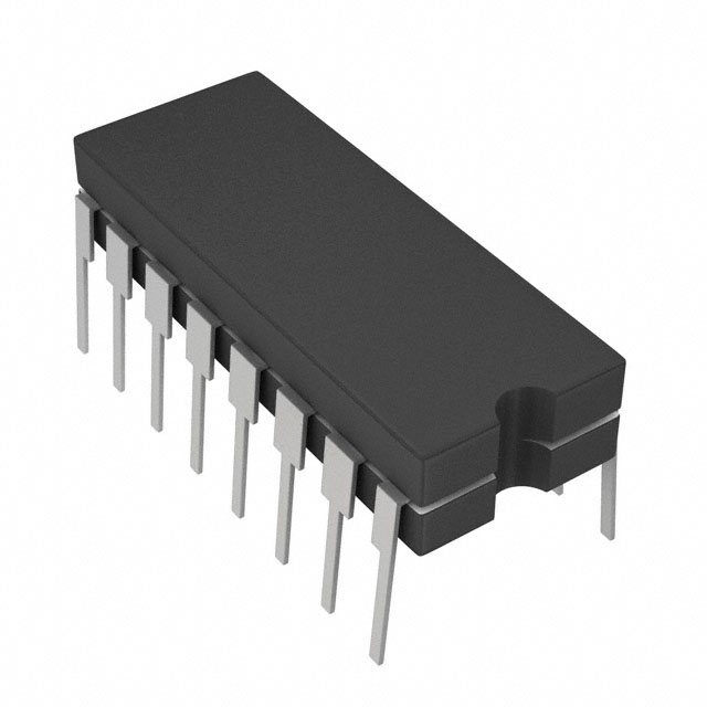
GDIP1-T16 or CDIP2-T16
16 LEAD CERDIP
J16
LP
2
CQCC1-N20
20 Pin Leadless Chip
L20
Absolute Maximum Ratings
Terminal Voltage
VCC for 01 ....................................................................................................... -0.3V to +6.0V
VCC for 02 ..................................................................................................................... +0.3V
VBATT for 01 .................................................................................................... -0.3V to +6.0V
GND for 02 .................................................................................................................... -0.3V
All other Inputs 1/ ................................................................................. -0.3V to (VOUT+0.5V)
Input Current
VCC ............................................................................................................................... 200mA
VBATT .............................................................................................................................. 50mA
GND ............................................................................................................................... 20mA
Output Current
VOUT .................................................................................................. Short-circuit protected
All other outputs ........................................................................................................... 20mA
Rate of Rise, VCC, VBATT ................................................................................................ 100V/µs
Lead Temperature (soldering, 10 seconds) ...................................................................... +300°C
Storage Temperature ......................................................................................... -65°C to +160°C
Continuous Power Dissipation ................................................................................... TA=+70°C
16 lead CERDIP(derate 10.0mW/°C above +70°C) ................................................. 800mW
20 lead LCC(derate 9.1mW/°C above +70°C) ......................................................... 727mW
Junction Temperature TJ ............................................................................................ +150°C
Thermal Resistance, Junction to Case, ΘJC:
Case Outline 16 lead CERDIP................................................................... 50°C/W
Case Outline 20 leadless Chip carrier ....................................................... 20°C/W
Thermal Resistance, Junction to Ambient, ΘJA:
Case Outline 16 lead CERDIP................................................................. 100°C/W
Case Outline 20 leadless Chip carrier ..................................................... 110°C/W
Recommended Operating Conditions
Ambient Operating Range (TA) ............................................................. -55°C to +125°C
Supply Voltage Range (VCC) ....................................................................... +3.0V to 5.5V
NOTE 1: The input voltage limits on PFI and WDI may be exceeded if the input current is limited to
less than 10mA.
Stresses beyond those listed under “Absolute Maximum Ratings” may cause permanent damage to the device.
These are stress ratings only, and functional operation of the device at these or any other conditions beyond
those indicated in the operational sections of the specifications is not implied. Exposure to absolute maximum
rating conditions for extended periods may affect device reliability.
----------------------------
Electrical Characteristics of MAX696/697/883B
for /883B and SMD 5962-93125
19-2554
Page 2 of
Rev. D
8
�TABLE 1. ELECTRICAL TESTS:
TEST
Operating Voltage
Range
Symbol
CONDITIONS
-55 °C ≤TA≤+125°C 2/
Unless otherwise specified
Group A
Subgroup
Device
type
VCC
Limits
Min
Limits
Max
1,2,3
01
02
3.2
3.0
5.5
5.5
2.0
1,2,3
01
02
VCC-0.3
400
1,2,3
01
Units
V
VBATT
Supply Current
ICC
BATTERY-BACKUP SWITCHING
Output Voltage
VOUT
IOUT=1mA
Output VoltageBattery-Backup
Mode
Supply Current
(Excludes IOUT)
BATT
IOUT=50mA
IOUT=250µA, VCCVCC>VBATT+1V
Leakage Current
SLKG
Battery-Switchover BATT
Power-Up or Power-Down
Threshold, VCC to
SWTH
VBATT
BATT ON Output
BATT
ISINK=1.6mA
Voltage
ONOUT
BATT
BATT ON Output
BATT ON = VOUT
ONIOS
Short-Circuit
Current
BATT ON =0V, VCC=0V
RESET AND WATCHDOG TIMING
Low-Line
LLIN
VCC=5V, 3V
Threshold
Reset Timeout
RDEL
OSC SEL High, VCC=5V
Delay
Watchdog Timeout WDINT
Long period, VCC=5V
Period, Internal
Oscillator
Short period, VCC=5V
ISOURCE=1µA, VCC=5V
mA
7
10
1
10
01
1
2,3
1,2,3
01
All
1,2,3
01
1,2,3
01
-0.10
-1.00
-200
0.02
0.02
+200
µA
µA
mV
0.4
V
60
mA
0.5
25
µA
1,2,3
All
1.25
1.35
V
9
10,11
9
10,11
All
35
31
1.00
0.90
70
78
2.25
2.42
ms
70
62
3840
140
154
4097
768
200
300
3.5
1025
sec
All
9
10,11
Long period
Short period
VIL=0.4V, VIH=4.0V, VCC=5V
µA
9,10,11
All
9
10,11
9,10,11
All
Electrical Characteristics of MAX696/697/883B
for /883B and SMD 5962-93125
All
19-2554
Page 3 of
ms
Clock
Cycles
ns
V
Rev. D
8
�TEST
______
RESET Output
Voltage
_________
LOWLINE Output
Voltage
RESET Output
Voltage
____
WDO Output
Voltage High
____
WDO Output
Voltage Low
Output ShortCircuit Current
WDI Input
Threshold Logic
Low
WDI Input
Threshold Logic
High
Symbol
_
RVOL
__
LLVOH
__
LLVOL
CONDITIONS
2/
-55 °C ≤TA≤+125°C
Unless otherwise specified
Device
type
ISINK=1.6mA
Limits
Min
Limits
Max
All
0.4
01
0.4
1,2,3
ISINK=400µA, VCC=0V
ISOURCE=1µA, VCC=5V
Units
V
3.5
All
V
1,2,3
0.4
ISINK=800µA
ISOURCE=1µA, VCC=5V
3.5
V
RVOH
1,2,3
RVOL
____
WDO
All
0.4
ISINK=1.6mA
ISOURCE=1µA, VCC=5V
1,2,3
All
3.5
V
VOH
____
WDO
2,3
ISINK=800µA
0.4
V
25
µA
0.8
0.4
V
VOL
WDIVIL
_____ ______
RESET, WDO, RESET,
_________
LOWLINE
VCC=5V
NOTE 3
WDIVIH
VCC=5V
IOS
NOTE 3
1,2,3
All
1.0
1
2,3
All
1
01
02
3.5
3.8
2,3
All
01
02
All
4.0
V
WDI=VOUT
WDI=VCC
WDI=0V
WDI Input Current
Group A
Subgroup
1
50
50
-50
µA
WDIIN
WDI=VOUT
WDI=VCC
WDI=0V
POWER-FAIL DETECTOR
PFI Input
PFIVIN
Threshold
PFILIN
PFI-LLIN
Threshold
Difference
PFI Input Current
PFIIN
LLIN Input
LLIN1
Current
___
___
PFOVOH
PFO Output
Voltage
___
PFOVOL
___
___
PFOIOS
PFO Short-Circuit
Source Current
----------------------------
2,3
01
02
All
80
80
-80
VCC=3V, 5V
1,2,3
All
1.2
1.4
V
VCC=3V, 5V
1
All
-50
50
mV
1,2,3
1,2,3
All
All
-25
-500
-25
3.5
25
25
25
nA
nA
ISOURCE=1µA, VCC=5V
1
All
ISINK=1.6mA
___
PFI=VIH, PFO=0V
V
2,3
1,2,3
Electrical Characteristics of MAX696/697/883B
for /883B and SMD 5962-93125
0.4
All
1.0
25
19-2554
Page 4 of
µA
Rev. D
8
�TEST
Symbol
CHIP-ENABLE GATING
__
__
CE IN Threshold
CEVIL
Logic Low
__
__
CE IN Threshold
CEVIH
Logic High
__
__
CE INPI
CE IN Pull-Up
Current
__
__
CEVOH
CE OUT Output
Voltage High
__
__
CE Output Voltage CEVOL
Low
__
___
CE Propagation
tPDCE
Delay
OSCILLATOR
OSC IN Input
OSCIIN
Current
OSC SEL Input
OSC
Pull-Up Current
SELIN
OSC IN Frequency OSC
Range
INfrq
OSC IN Frequency OSCIN
CONDITIONS
-55 °C ≤TA≤+125°C 2/
Unless otherwise specified
Group A
Subgroup
Device
type
Limits
Min
Limits
Max
1
0.8
02
V
2,3
1
VCC=5V
0.4
3.0
02
V
2,3
3.5
1,2,3
02
1,2,3
02
1.0
25
V
VOUT-0.05
ISOURCE=1µA
1,2,3
02
0.4
9
VCC=5V
ns
250
10,11
OSC SEL=0V, VCC=5V
OSC SEL=0V, COSC=47pF
NOTE 4
V
150
02
VCC=5V
µA
VOUT-0.5
ISOURCE=800µA
ISINK=1.6mA
Units
25
µA
1
25
µA
All
0
250
kHz
All
4
1,2,3
All
1,2,3
All
9,10,11
9
kHz
NOTE 2: VCC=full operating range, VBATT=+2.8V.
NOTE 3: WDI is guaranteed to be in the mid-level (inactive) state if WDI is floating and VCC is in the operating
range. WDI is internally biased to 38% of VCC with an impedance of approximately 125kΩ
NOTE 4: Typical for design purposes only but not tested.
01
01
02
02
Package
16 pin CERDIP
20 pin LCC
16 pin CERDIP
20 pin LCC
----------------------------
ORDERING INFORMATION:
MAX696MJE/883B
MAX696MLP/883B
MAX697MJE/883B
MAX697MLP/883B
SMD NUMBER
5962-9312502MEA
5962-9312502M2C
5962-9312501MEA
5962-9312501M2C
Electrical Characteristics of MAX696/697/883B
for /883B and SMD 5962-93125
19-2554
Page 5 of
Rev. D
8
�TERMINAL CONNECTIONS:
MAX696
MAX696
J16
L20
1
VBATT
NC
2
VOUT
VBATT
3
VCC
VOUT
4
GND
VCC
5
BATT ON
GND
6
_________
NC
LOWLINE
7
OSC IN
BATT ON
8
OSC SEL
9
PFI
10
OSC SEL
11
12
____
PFO
WDI
NC
13
LLIN
14
____
WDO
______
RESET
RESET
____
PFO
WDI
15
16
17
18
19
20
---------------------------
_________
LOWLINE
OSC IN
NC
PFI
NC
NC
LLIN
MAX697
J16
TEST
NC
VCC
LLIN
GND
_________
LOWLINE
MAX697
L20
NC
TEST
NC
VCC
LLIN
NC
GND
OSC IN
OSC SEL
_________
LOWLINE
PFI
____
PFO
WDI
__
CE OUT
__
CE IN
____
WDO
______
RESET
RESET
____
WDO
______
RESET
RESET
Electrical Characteristics of MAX696/697/883B
for /883B and SMD 5962-93125
OSC IN
OSC SEL
NC
PFI
____
PFO
WDI
__
CE OUT
NC
__
CE IN
____
WDO
______
RESET
RESET
19-2554
Page 6 of
Rev. D
8
�QUALITY ASSURANCE
Sampling and inspection procedures shall be in accordance with MIL-Prf-38535, Appendix A as specified in MilStd-883.
Screening shall be in accordance with Method 5004 of Mil-Std-883. Burn-in test Method 1015:
1. Test Condition, A, B, C, or D.
2. TA = +125°C minimum.
3. Interim and final electrical test requirements shall be specified in Table 2.
Quality conformance inspection shall be in accordance with Method 5005 of Mil-Std-883, including Groups A, B,
C, and D inspection.
Group A inspection:
1. Tests as specified in Table 2.
2. Selected subgroups in Table 1, Method 5005 of Mil-Std-883 shall be omitted.
Group C and D inspections:
a. End-point electrical parameters shall be specified in Table 1.
b. Steady-state life test, Method 1005 of Mil-Std-883:
1. Test condition A, B, C, D.
2. TA = +125°C, minimum.
3. Test duration, 1000 hours, except as permitted by Method 1005 of Mil-Std-883.
TABLE 2.
ELECTRICAL TEST REQUIREMENTS
Mil-Std-883 Test Requirements
Interim Electric Parameters
Method 5004
Final Electrical Parameters
Method 5005
Group A Test Requirements
Method 5005
Group C and D End-Point Electrical Parameters
Method 5005
*
Subgroups
per Method 5005, Table 1
1
1*, 2, 3, 9, 10, 11
1, 2, 3, 9, 10, 11
1
PDA applies to Subgroup 1 only.
---------------------------
Electrical Characteristics of MAX696/697/883B
for /883B and SMD 5962-93125
19-2554
Page 7 of
Rev. D
8
�


 工商网监
湘ICP备2023018690号
工商网监
湘ICP备2023018690号
