Not Recommended for New Designs
This product was manufactured for Maxim by an outside wafer foundry
using a process that is no longer available. It is not recommended for
new designs. The data sheet remains available for existing users.
A Maxim replacement or an industry second-source may be available.
Please see the QuickView data sheet for this part or contact technical
support for assistance.
For further information, contact Maxim’s Applications Tech Support.
�19-0149; Rev 2; 9/95
5V/3.3V/3V 2A Step-Down, PWM,
Switch-Mode DC-DC Regulators
The MAX727/MAX728/MAX729 are monolithic, bipolar,
pulse-width modulation (PWM), switch-mode, step-down
DC-DC regulators. Each is rated at 2A. Very few external
components are needed for standard operation because
the power switch, oscillator, feedback, and control circuitry
are all on-chip. Employing a classic buck topology, these
regulators perform high-current step-down functions.
These regulators have excellent dynamic and transient
response characteristics, while featuring cycle-by-cycle current limiting to protect against overcurrent faults and shortcircuit output faults. They also have a wide 8V to 40V input
range.
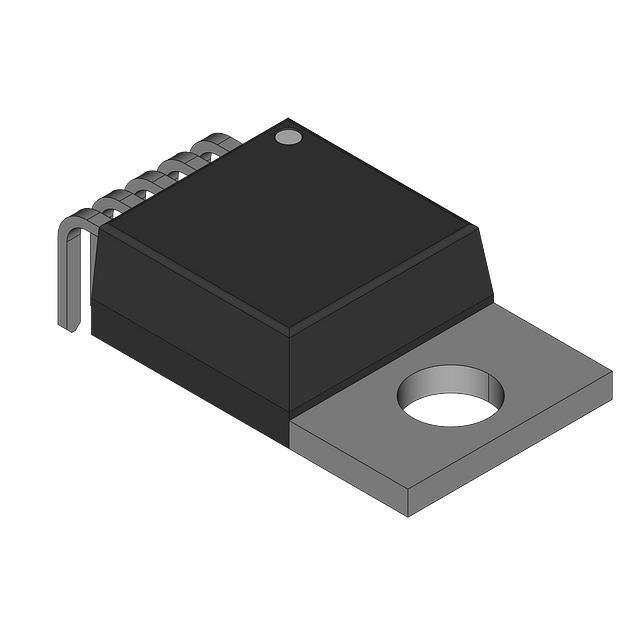
Each regulator is available in a 5-pin TO-220 package.
These devices have a preset 100kHz oscillator frequency
and a preset current limit of 2.6A. See the MAX724/
MAX726 data sheet for more applications information.
_______________________Applications
Distributed Power from High-Voltage Buses
High-Current, High-Voltage Step-Down Applications
Multiple-Output Buck Converter
__________Typical Operating Circuit
___________________________Features
♦ Input Range: Up to 40V
♦ 2A On-Chip Power Switch
♦ Fixed Outputs: 5V (MAX727)
3.3V (MAX728)
3V (MAX729)
♦ 100kHz Switching Frequency
♦ Excellent Dynamic Characteristics
♦ Few External Components
♦ 8.5mA Quiescent Current
♦ TO-220 Package
______________Ordering Information
PART
TEMP. RANGE
PIN-PACKAGE
MAX727CCK
0°C to +70°C
5 TO-220
MAX727ECK
-40°C to +85°C
5 TO-220
MAX728CCK
0°C to +70°C
5 TO-220
MAX728ECK
-40°C to +85°C
5 TO-220
MAX729CCK
0°C to +70°C
5 TO-220
MAX729ECK
-40°C to +85°C
5 TO-220
__________________Pin Configuration
FRONT VIEW
INPUT
8V TO 40V
100µH
VIN
VSW
OUTPUT
5V AT 2A
220µF
MAX727
VC
MBR745
SENSE
2.7k
GND
0.01µF
470µF
MAX727
MAX728
MAX729
5
4
VIN
3
2
GND
1
SENSE
VSW
VC
5-PIN TO-220
CASE IS CONNECTED TO GROUND. STANDARD PACKAGE HAS STAGGERED LEADS.
CONTACT FACTORY FOR STRAIGHT LEADS.
STEP-DOWN CONVERTER
________________________________________________________________ Maxim Integrated Products
Call toll free 1-800-998-8800 for free samples or literature.
1
MAX727/MAX728/MAX729
_______________General Description
�MAX727/MAX728/MAX729
5V/3.3V/3V 2A Step-Down, PWM,
Switch-Mode DC-DC Regulators
ABSOLUTE MAXIMUM RATINGS
Input Voltage . . . . . . . . . . . . . . . . . . . . . . . . . . . . . . . . . . . . . . . . . . . . . . . . . . 45V
Switch Voltage with Respect to Input Voltage. . . . . . . . . . . . . . . . 50V
Switch Voltage with Respect to GND Pin (VSW negative)
(Note 1) . . . . . . . . . . . . . . . . . . . . . . . . . . . . . . . . . . . . . . . . . . . . . . . . . . . . . 35V
SENSE Pin Voltage . . . . . . . . . . . . . . . . . . . . . . . . . . . . . . . . . . . -0.3V, +10V
Operating Temperature Ranges
MAX72_CCK . . . . . . . . . . . . . . . . . . . . . . . . . . . . . . . . . . . . . 0°C to +70°C
MAX72_ECK. . . . . . . . . . . . . . . . . . . . . . . . . . . . . . . . . . . . -40°C to +85°C
Junction Temperature Ranges:
MAX72_CCK . . . . . . . . . . . . . . . . . . . . . . . . . . . . . . . . . . . . 0°C to +125°C
MAX72_ECK . . . . . . . . . . . . . . . . . . . . . . . . . . . . . . . . . . - 40°C to +125°C
Storage Temperature Range . . . . . . . . . . . . . . . . . . . -65°C to +160°C
Lead Temperature (soldering, 10sec). . . . . . . . . . . . . . . . . . . . +300°C
Stresses beyond those listed under “Absolute Maximum Ratings” may cause permanent damage to the device. These are stress ratings only, and functional
operation of the device at these or any other conditions beyond those indicated in the operational sections of the specifications is not implied. Exposure to
absolute maximum rating conditions for extended periods may affect device reliability.
ELECTRICAL CHARACTERISTICS
(VIN = 25V, Tj = TMIN to TMAX, unless otherwise noted.)
PARAMETER
CONDITIONS
MIN
Input Supply Voltage Range
Switch-On Voltage (Note 2)
Switch-Off Leakage
Supply Current (Note 3)
TYP
8.0
MAX
UNITS
40.0
V
ISW = 0.5A
1.2
ISW = 2A
1.7
VIN = 25V, VSW = 0V
Tj = +25°C
150
VIN = 40V, VSW = 0V
Tj = +25°C
250
VIN ≤ 40V, VSENSE = 5.5V
8.5
11
Normal Mode
7.3
8.0
Tj ≥ 0°C
3.5
4.8
Tj < 0°C
3.5
5.0
3.2
Minimum Supply Voltage
Start-Up Mode (Note 4)
Switch-Current Limit (Note 5)
2.0
2.6
Maximum Duty Cycle
85
90
Tj = +25°C
90
100
Tj ≤ +125°C
85
Switching Frequency
VOUT = VSENSE = 0V (Note 5) Tj = +25°C
Switching Frequency Line Regulation
8V ≤ VIN ≤ 40V
Error-Amplifier Voltage Gain
1V ≤ VC ≤ 4V
Error-Amplifier Transconductance
V
µA
mA
V
A
%
110
120
kHz
0.10
%/V
20
0.03
Tj = +25°C
2000
V/V
Tj = +25°C
3000
5000
9000
µmho
Error-Amplifier Source Current
VSENSE = VOUT - 10%
Tj = +25°C
100
140
225
µA
Error-Amplifier Sink Current
VSENSE = VOUT + 10%
Tj = +25°C
0.6
1.0
1.7
mA
2
_______________________________________________________________________________________
�5V/3.3V/3V 2A Step-Down, PWM,
Switch-Mode DC-DC Regulators
MAX727/MAX728/MAX729
ELECTRICAL CHARACTERISTICS (continued)
(VIN = 25V, Tj = TMIN to TMAX, unless otherwise noted.)
PARAMETER
CONDITIONS
MAX727
MAX728
MAX729
MAX727
MAX728
MAX729
SENSE Voltage
VC = 2V
SENSE Pin Divider Resistance
Tj = +25°C
Output Voltage Tolerance
VOUT (nominal) = 5V (MAX727),
3.3V (MAX728), or 3V (MAX729); Tj = +25°C
all conditions of input voltage,
Tj = TMIN to
output voltage, and load
TMAX
current
MIN
TYP
MAX
4.85
3.20
2.90
3.0
2.5
2.2
5.00
3.30
3.00
5.0
4.2
3.8
5.15
3.40
3.10
8.0
7.0
6.5
±0.5
±2.0
±1.0
±3.0
0.005
0.020
UNITS
V
kΩ
%
Output Voltage Line Regulation
8V ≤ VIN ≤ 40V
VC Voltage
0% duty cycle
Tj = +25°C
1.5
V
VC Voltage Temperature Coefficient
0% duty cycle
Tj = TMIN to TMAX
-4
mV/°C
Thermal Resistance Junction to Case
(Note 6)
4.0
%/V
°C/W
Note 1: Do not exceed switch-to-input voltage limitation.
Note 2: For switch currents between 1A and 2A, maximum switch-on voltage can be calculated via linear interpolation.
Note 3: By setting the SENSE pin to 5.5V, the VC pin is forced to its low clamp level and the switch duty cycle is forced to zero,
approximating the zero load condition.
Note 4: For proper regulation, total voltage from VIN to GND must be ≥ 8V after start-up.
Note 5: To avoid extremely short switch-on times, the switch frequency is internally scaled down when VSENSE is less than 2.6V
(MAX727), 2.0V (MAX728), or 1.8V (MAX729). Switch current limit is tested with VSENSE adjusted to give a 1µs minimum
switch-on time.
Note 6: Guaranteed, not production tested.
______________________________________________________________Pin Description
PIN
NAME
FUNCTION
1
SENSE
SENSE Input is the internal error amplifier's input, and should be directly connected to VOUT.
SENSE also aids current limiting by reducing oscillator frequency when VOUT is low.
2
VC
Error-Amplifier Output. A series RC network connected to this pin compensates the
MAX727/MAX728/MAX729. Output swing is limited to about 5.8V in the positive direction and
-0.7V in the negative direction. VC can also synchronize the MAX727/MAX728/MAX729 to an
external TTL clock in the 115kHz to 170kHz range. See MAX724/MAX726 data sheet.
3
GND
Ground requires a short, low-noise connection to ensure good load regulation. The internal reference is referred to GND, so errors at this pin are multiplied by the error amplifier.
4
VSW
Internal Power Switch Output. The Switch output can swing 35V below ground and is rated for 2A.
5
VIN
VIN supplies power to the internal circuitry and also connects to the collector of the internal power
switch. VIN must be bypassed with a low-ESR capacitor, typically 200µF or 220µF.
_______________________________________________________________________________________
3
�MAX727/MAX728/MAX729
5V/3.3V/3V 2A Step-Down, PWM,
Switch-Mode DC-DC Regulators
________________________________________________________Package Information
DIM
A
E
F
φP
Q
H1
D
L2
J1
A
B
C1
D
E
e
F
H1
J1
J2
J3
L
L1
L2
φP
Q
INCHES
MAX
MIN
0.190
0.140
0.040
0.015
0.022
0.014
0.650
0.560
0.420
0.380
0.067 BSC
0.055
0.045
0.270
0.230
0.115
0.080
0.185
0.170
0.335
0.327
0.200
0.170
0.340
0.260
0.720
0.700
0.161
0.139
0.120
0.100
21-005-
L
L1
5-PIN TO-220
(STAGGERED LEAD)
PACKAGE
C1
B
J2
e
MILLIMETERS
MIN
MAX
3.56
4.82
0.38
1.01
0.41
0.50
14.23
16.51
9.66
10.66
1.70 BSC
1.14
1.39
5.85
6.85
2.04
2.92
4.32
4.70
8.31
8.51
4.32
5.08
6.60
8.64
17.78
18.29
3.54
4.08
2.54
3.04
J3
DIM
A
E
F
φP
Q
H1
D
J1
A
B
C1
D
E
e
F
H1
J1
L
φP
Q
INCHES
MAX
MIN
0.190
0.140
0.040
0.015
0.022
0.014
0.650
0.560
0.420
0.380
0.067 BSC
0.055
0.045
0.270
0.230
0.115
0.080
0.580
0.500
0.161
0.139
0.120
0.100
MILLIMETERS
MIN
MAX
3.56
4.82
0.38
1.01
0.41
0.50
14.23
16.51
9.66
10.66
1.70 BSC
1.14
1.39
5.85
6.85
2.04
2.92
12.70
14.73
3.54
4.08
2.54
3.04
21-4737-
L
B
C1
e
5-PIN TO-220
(STRAIGHT LEAD)
PACKAGE
CONTACT FACTORY FOR AVAILABILITY
Maxim cannot assume responsibility for use of any circuitry other than circuitry entirely embodied in a Maxim product. No circuit patent licenses are
implied. Maxim reserves the right to change the circuitry and specifications without notice at any time.
4 ___________________Maxim Integrated Products, 120 San Gabriel Drive, Sunnyvale, CA 94086 (408) 737-7600
© 1995 Maxim Integrated Products
Printed USA
is a registered trademark of Maxim Integrated Products.
�


 工商网监
湘ICP备2023018690号
工商网监
湘ICP备2023018690号
