EVALUATION KIT AVAILABLE
Click here to ask about the production status of specific part numbers.
MAX77812
20A User-Configurable
Quad-Phase Buck Converter
General Description
The MAX77812 is a quad-phase high-efficiency stepdown (buck) converter capable of delivering up to 20A
of maximum current. Programmable startup/shutdown
sequence and user-selectable phase configurations make
the MAX77812 ideal for powering the latest generations
of processors. With high-efficiency and small solution
size, the MAX77812 is optimized for space constrained
single-cell battery powered applications.
The MAX77812 uses an adaptive on-time PWM control
scheme and it has SKIP and low-power SKIP modes for
improved light-load efficiency. A programmable current
limit reduces the overall solution footprint by optimizing
inductors size. Differential sensing provides high output
voltage accuracy, while enhanced transient response
(ETR) allows fast output voltage adjustments to load transients. Programmable soft-start/stop and ramp-up/down
slew rate provides control over an inrush current as the
regulator transitions between operating states.
A 3.4MHz high-speed I2C or 30MHz SPI interface with
dedicated logic inputs provide full configurability and
control for system power optimization.
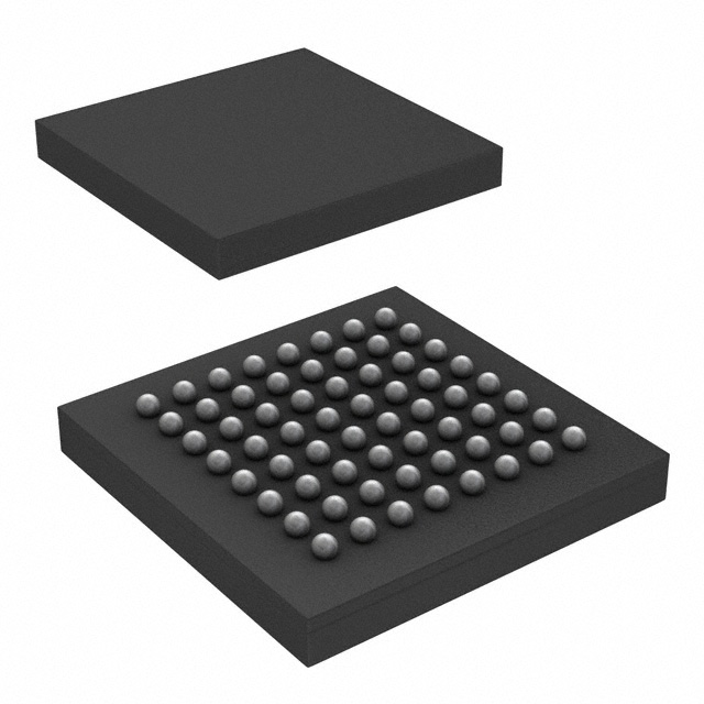
The MAX77812 is available in 3.408mm x 3.368mm,
64-bump 0.4mm pitch wafer-level package (WLP).
Benefits and Features
●● 20A Maximum Output Current (5A per Phase)
●● VIN Range: 2.5V to 5.5V
●● VOUT Range: 0.250V to 1.525V with 5mV Steps
●● ±0.5% Initial Output Accuracy with Differential Sensing
●● 5 User-Selectable Phase Configurations
●● 91% Peak Efficiency (VIN = 3.8V, VOUT = 1.1V)
●● Auto (SKIP/PWM) and Forced PWM Modes
●● Enhanced Load Transient Response
●● Programmable Ramp-Up/Down Slew Rates
●● Programmable Startup/Shutdown Sequence
●● UVLO, Short-Circuit, and Thermal Protections
●● 2 User-Programmable General-Purpose Inputs
●● 3.4MHz High Speed I2C and 30MHz SPI Interface
●● 3.408mm x 3.368mm, 64-Bump WLP Package
Applications
●●
●●
●●
●●
CPU/GPU, FPGAs, and DSPs Power Supply
AR/VR Headsets and Game Consoles
Li-ion Battery Powered Equipment
Space Constrained Portable Electronics
Ordering Information appears at end of data sheet.
Typical Application Circuit
VSYS
2.5V to 5.5V
VVIO
VSYS
2.5V to 5.5V
19-8541; Rev 11; 12/20
IN12
SYS
DGND
AGND
CE
VIO
MAX77812
MULTI-PHASE
BUCK
IRQB
SCL
SDA/MOSI
MISO
SCS
I2C_SPI_SEL
EN
LPM
WDTRSTB_IN
GPI0
GPI1
PH_CFG0
PH_CFG1
PH_CFG2
LX1
SNS1P
SNS1N
PGND1
VSYS
2.5V to 5.5V
0.25V to 1.525V
10A
LX2
SNS2P
SNS2N
PGND2
IN34
LX3
SNS3P
SNS3N
PGND3
LX4
SNS4P
SNS4N
PGND4
1Φ
+
1Φ
+
1Φ
+
1Φ
2Φ
5A
5A
5A
5A
10A
2Φ
+
1Φ
+
1Φ
10A
5A
5A
+
VSYS
2.5V to 5.5V
2Φ
10A
+
0.25V to 1.525V
5A
0.25V to 1.525V
5A
3Φ
1Φ
4Φ
15A
5A
20A
PHASE-CONFIGURABLE
QUAD-OUTPUT
�MAX77812
20A User-Configurable
Quad-Phase Buck Converter
Absolute Maximum Ratings
SYS, VIO to AGND................................................-0.3V to +6.0V
DGND to AGND.....................................................-0.3V to +0.3V
SCL, SDA/MOSI, MISO, SCS, IRQB, CE, EN, LPM, GPI0, GPI1,
WDTRSTB_IN to DGND...................... -0.3V to (VVIO + 0.3V)
PH_CFG0, PH_CFG1, PH_CFG2,
I2C_SPI_SEL to AGND....................... -0.3V to (VSYS + 0.3V)
IN12, IN34 to PGNDx.............................. -0.3V to (VSYS + 0.3V)
LX1/2/3/4 to PGNDx..................................-0.3V to (VIN_ + 0.3V)
LX1/2/3/4 to PGNDx (Pulsed +165°C
1
TJCT_140C
—
0: Junction Temperature (TJCT) ≤ +140°C
1: Junction Temperature (TJCT) > +140°C
0
TJCT_120C
—
0: Junction Temperature (TJCT) ≤ +120°C
1: Junction Temperature (TJCT) > +120°C
www.maximintegrated.com
DESCRIPTION
Maxim Integrated │ 47
�MAX77812
20A User-Configurable
Quad-Phase Buck Converter
EN_CTRL Regulator Enable Control Register
ADDRESS
MODE
0x06
R/W
BIT
NAME
TYPE: O
POR
RESET VALUE: 0x00
DESCRIPTION
7
EN_M4_LPM
0
0: Disable BUCK Master 4 low power mode.
1: Enable BUCK Master 4 low power mode.
6
EN_M4
0
0: Disable BUCK Master 4 output.
1: Enable BUCK Master 4 output (‘OR’ logic with GPIx input).
5
EN_M3_LPM
0
0: Disable BUCK Master 3 low power mode.
1: Enable BUCK Master 3 low power mode.
4
EN_M3
0
0: Disable BUCK Master 3 output.
1: Enable BUCK Master 3 output (‘OR’ logic with GPIx input).
3
EN_M2_LPM
0
0: Disable BUCK Master 2 low power mode.
1: Enable BUCK Master 2 low power mode.
2
EN_M2
0
0: Disable BUCK Master 2 output.
1: Enable BUCK Master 2 output (‘OR’ logic with GPIx input).
1
EN_M1_LPM
0
0: Disable BUCK Master 1 low power mode.
1: Enable BUCK Master 1 low power mode.
0
EN_M1
0
0: Disable BUCK Master 1 output.
1: Enable BUCK Master 1 output (‘OR’ logic with GPIx input).
STUP_DLY1 Global Startup Delay Setting Register 1
ADDRESS
MODE
0x07
R/W
TYPE: O (OTP)
BIT
NAME
POR
7
DLY_STEP
0
6:5
RESERVED
00
4:0
M2_STUP_DLY[4:0]
www.maximintegrated.com
0 0000
RESET VALUE: 0x00
DESCRIPTION
Delay Time Step Selection
0: 1ms
1: 2ms
BUCK Master 2 Startup Delay Time Setting (Delay from Rising Edge
of EN Pin or GLB_EN)
0 0000b = 0ms
0 0001b = 1 x DLY_STEP
0 0010b = 2 x DLY_STEP
·
·
·
·
·
·
1 1110b = 30 x DLY_STEP
1 1111b = 31 x DLY_STEP
Maxim Integrated │ 48
�MAX77812
20A User-Configurable
Quad-Phase Buck Converter
STUP_DLY2 Global Startup Delay Setting Register 2
ADDRESS
MODE
0x08
R/W
TYPE: O (OTP)
BIT
NAME
POR
7:5
RESERVED
000
4:0
M3_STUP_DLY[4:0]
0 0000
RESET VALUE: 0x00
DESCRIPTION
BUCK Master 3 Startup Delay Time Setting (Delay from Rising Edge
of EN Pin or GLB_EN)
0 0000b = 0ms
0 0001b = 1 x DLY_STEP
0 0010b = 2 x DLY_STEP
·
·
·
·
·
·
1 1110b = 30 x DLY_STEP
1 1111b = 31 x DLY_STEP
STUP_DLY3 Global Startup Delay Setting Register 3
ADDRESS
MODE
0x09
R/W
TYPE: O (OTP)
BIT
NAME
POR
7:5
RESERVED
000
4:0
M4_STUP_DLY[4:0]
0 0000
RESET VALUE: 0x00
DESCRIPTION
BUCK Master 4 Startup Delay Time Setting (Delay from Rising Edge
of EN Pin or GLB_EN)
0 0000b = 0ms
0 0001b = 1 x DLY_STEP
0 0010b = 2 x DLY_STEP
·
·
·
·
·
·
1 1110b = 30 x DLY_STEP
1 1111b = 31 x DLY_STEP
SHDN_DLY1 Global Shutdown Delay Setting Register 1
ADDRESS
MODE
0x0A
R/W
TYPE: O
BIT
NAME
POR
7:5
RESERVED
000
4:0
M1_SHDN_DLY[4:0]
www.maximintegrated.com
0 0000
RESET VALUE: 0x00
DESCRIPTION
BUCK Master 1 Shutdown Delay Time Setting (Delay from Falling
Edge of EN Pin or GLB_EN)
0 0000b = 0ms
0 0001b = 1 x DLY_STEP
0 0010b = 2 x DLY_STEP
·
·
·
·
·
·
1 1110b = 30 x DLY_STEP
1 1111b = 31 x DLY_STEP
Maxim Integrated │ 49
�MAX77812
20A User-Configurable
Quad-Phase Buck Converter
SHDN_DLY2 Global Shutdown Delay Setting Register 2
ADDRESS
MODE
0x0B
R/W
TYPE: O
BIT
NAME
POR
7:5
RESERVED
000
4:0
M2_SHDN_DLY[4:0]
0 0000
RESET VALUE: 0x00
DESCRIPTION
BUCK Master 2 Shutdown Delay Time Setting (Delay from Falling
Edge of EN Pin or GLB_EN)
0 0000b = 0ms
0 0001b = 1 x DLY_STEP
0 0010b = 2 x DLY_STEP
·
·
·
·
·
·
1 1110b = 30 x DLY_STEP
1 1111b = 31 x DLY_STEP
SHDN_DLY3 Global Shutdown Delay Setting Register 3
ADDRESS
MODE
0x0C
R/W
TYPE: O
BIT
NAME
POR
7:5
RESERVED
000
4:0
M3_SHDN_DLY[4:0]
0 0000
RESET VALUE: 0x00
DESCRIPTION
BUCK Master 3 Shutdown Delay Time Setting (Delay from Falling
Edge of EN Pin or GLB_EN)
0 0000b = 0ms
0 0001b = 1 x DLY_STEP
0 0010b = 2 x DLY_STEP
·
·
·
·
·
·
1 1110b = 30 x DLY_STEP
1 1111b = 31 x DLY_STEP
SHDN_DLY4 Global Shutdown Delay Setting Register 4
ADDRESS
MODE
0x0D
R/W
TYPE: O
BIT
NAME
POR
7:5
RESERVED
000
4:0
M4_SHDN_DLY[4:0]
www.maximintegrated.com
0 0000
RESET VALUE: 0x00
DESCRIPTION
BUCK Master 4 Shutdown Delay Time Setting (Delay from Falling
Edge of EN Pin or GLB_EN)
0 0000b = 0ms
0 0001b = 1 x DLY_STEP
0 0010b = 2 x DLY_STEP
·
·
·
·
·
·
1 1110b = 30 x DLY_STEP
1 1111b = 31 x DLY_STEP
Maxim Integrated │ 50
�MAX77812
20A User-Configurable
Quad-Phase Buck Converter
WDTRSTB_DEB WDTRSTB_IN Input Debounce Time Setting Register
ADDRESS
MODE
0x0E
R/W
TYPE: O
BIT
NAME
POR
7:3
RESERVED
0000 0
2:0
WDT_DEB[2:0]
010
RESET VALUE: 0x02
DESCRIPTION
WDTRSTB_IN Debounce Time Setting
000b = 0ms
001b = 0.8ms
010b = 1.6ms
011b = 3.2ms
100b = 6.4ms
101b = 12.8ms
111b = 51.2ms
GPI_FUNC GPI Function Selection Register
ADDRESS
MODE
0x0F
R/W
BIT
7:4
3:0
NAME
GPI1_FUNC[3:0]
GPI0_FUNC[3:0]
www.maximintegrated.com
TYPE: O
POR
RESET VALUE: 0x43
DESCRIPTION
0100
GPI1 Function Selection
0000b: GLB_EN
1000b: M3_VSEL
0001b: M1_EN
1001b: M4_VSEL
0010b: M2_EN
1010b: GLB_LPM
0011b: M3_EN
1011b: M1_LPM
0100b: M4_EN
1100b: M2_LPM
0101b: GLB_VSEL 1101b: M3_LPM
0110b: M1_VSEL 1110b: M4_LPM
0111b: M2_VSEL
1111b: No Function
0011
GPI0 Function Selection
0000b: GLB_EN
1000b: M3_VSEL
0001b: M1_EN
1001b: M4_VSEL
0010b: M2_EN
1010b: GLB_LPM
0011b: M3_EN
1011b: M1_LPM
0100b: M4_EN
1100b: M2_LPM
0101b: GLB_VSEL 1101b: M3_LPM
0110b: M1_VSEL 1110b: M4_LPM
0111b: M2_VSEL
1111b: No Function
Maxim Integrated │ 51
�MAX77812
20A User-Configurable
Quad-Phase Buck Converter
GPI_DEB1 GPI Debounce Time Setting Register 1
ADDRESS
MODE
0x10
R/W
BIT
7:4
3:0
NAME
TYPE: O
POR
LPM_DEB[3:0]
EN_DEB[3:0]
RESET VALUE: 0x11
DESCRIPTION
0001
LPM Debounce Time Setting
0000b = 0µs
1000b = 512µs
0001b = 64µs
1001b = 576µs
0010b = 128µs
1010b = 640µs
0011b = 192µs
1011b = 704µs
0100b = 256µs
1100b = 768µs
0101b = 320µs
1101b = 832µs
0110b = 384µs
1110b = 896µs
0111b = 448µs
1111b = 960µs
0001
EN Debounce Time Setting
0000b = 0µs
1000b = 512µs
0001b = 64µs
1001b = 576µs
0010b = 128µs
1010b = 640µs
0011b = 192µs
1011b = 704µs
0100b = 256µs
1100b = 768µs
0101b = 320µs
1101b = 832µs
0110b = 384µs
1110b = 896µs
0111b = 448µs
1111b = 960µs
GPI_DEB2 GPI Debounce Time Setting Register 2
ADDRESS
MODE
0x11
R/W
BIT
7:4
3:0
NAME
GPI1_DEB[3:0]
GPI0_DEB[3:0]
www.maximintegrated.com
TYPE: O
POR
RESET VALUE: 0x11
DESCRIPTION
0001
GPI1 Debounce Time Setting
0000b = 0µs
1000b = 512µs
0001b = 64µs
1001b = 576µs
0010b = 128µs
1010b = 640µs
0011b = 192µs
1011b = 704µs
0100b = 256µs
1100b = 768µs
0101b = 320µs
1101b = 832µs
0110b = 384µs
1110b = 896µs
0111b = 448µs
1111b = 960µs
0001
GPI0 Debounce Time Setting
0000b = 0µs
1000b = 512µs
0001b = 64µs
1001b = 576µs
0010b = 128µs
1010b = 640µs
0011b = 192µs
1011b = 704µs
0100b = 256µs
1100b = 768µs
0101b = 320µs
1101b = 832µs
0110b = 384µs
1110b = 896µs
0111b = 448µs
1111b = 960µs
Maxim Integrated │ 52
�MAX77812
20A User-Configurable
Quad-Phase Buck Converter
GPI_PD_CTRL GPI Pulldown Resistor Control Register
ADDRESS
MODE
0x12
R/W
TYPE: O
RESET VALUE: 0x0F
BIT
NAME
POR
7:4
RESERVED
0000
DESCRIPTION
3
LPM_PD
1
LPM Input Pulldown Resistor Enable Setting
0: Disable
1: Enable
2
EN_PD
1
EN Input Pulldown Resistor Enable Setting
0: Disable
1: Enable
1
GPI1_PD
1
GPI1 Input Pulldown Resistor Enable Setting
0: Disable
1: Enable
0
GPI0_PD
1
GPI0 Input Pulldown Resistor Enable Setting
0: Disable
1: Enable
PROT_CFG Protection Configuration Register
ADDRESS
MODE
0x13
R/W
TYPE: O
BIT
NAME
POR
7
TSHDN_EN
1
6:3
RESERVED
000 0
2:0
UVLO_F[2:0]
010
RESET VALUE: 0x82
DESCRIPTION
Thermal Protection Enable Control
0: Disable (TSHDN_INT is not disabled)
1: Enable
VSYS UVLO Falling Threshold
000b = 1.95V
001b = 2.05V
010b = 2.15V
011b = 2.25V
100b = 2.35V
101b = 2.45V
110b = 2.55V
111b = Disabled
0x14: RESERVED
www.maximintegrated.com
Maxim Integrated │ 53
�MAX77812
20A User-Configurable
Quad-Phase Buck Converter
I2C_CFG I2C Configuration Register
ADDRESS
MODE
0x15
R/W
TYPE: O
RESET VALUE: 0x00
BIT
NAME
POR
7:4
RESERVED
NA
3:2
RESERVED
00
Write ‘00’
1
PAIR
0
Register Data Pair Mode
0: Disable (Sequential Mode)
1: Enable
0
HS Mode Extension
0: Disable HS mode extension (I2C Rev. 4 Compliant).
1: Enable HS mode extension.
(HS mode is extended during/after ‘STOP’ condition.)
0
HS_EXT
DESCRIPTION
0x16 – 0x1F: RESERVED
BUCK_INT Regulators Interrupt Register
ADDRESS
MODE
0x20
R/C
TYPE: S1
RESET VALUE: 0x00
BIT
NAME
POR
7:4
RESERVED
0000
DESCRIPTION
3
M4_POK_INT
0
1: BUCK Master 4 POK interrupt has triggered.
2
M3_POK _INT
0
1: BUCK Master 3 POK interrupt has triggered.
1
M2_POK _INT
0
1: BUCK Master 2 POK interrupt has triggered.
0
M1_POK _INT
0
1: BUCK Master 1 POK interrupt has triggered.
BUCK_INT_M BUCK Interrupt Mask Register
ADDRESS
MODE
0x21
R/W
TYPE: O
BIT
NAME
POR
7:4
RESERVED
0000
3
M4_POK _M
1
0: Enable M4_POK _INT.
1: Mask M4_POK _INT.
2
M3_POK_M
1
0: Enable M3_ POK_INT.
1: Mask M3_POK_INT.
1
M2_POK_M
1
0: Enable M2_ POK_INT.
1: Mask M2_POK_INT.
0
M1_POK_M
1
0: Enable M1_POK_INT.
1: Mask M1_POK_INT.
www.maximintegrated.com
RESET VALUE: 0x0F
DESCRIPTION
Maxim Integrated │ 54
�MAX77812
20A User-Configurable
Quad-Phase Buck Converter
BUCK_STAT BUCK Status Register
ADDRESS
MODE
0x22
R
TYPE: O
RESET VALUE: N/A
BIT
NAME
POR
7:4
RESERVED
0000
DESCRIPTION
3
M4_POK
0
BUCK Master 4 POK Status
2
M3_POK
0
BUCK Master 3 POK Status
1
M2_POK
0
BUCK Master 2 POK Status
0
M1_POK
0
BUCK Master 1 POK Status
M1_VOUT BUCK Master1 Output Voltage Setting Register
ADDRESS
MODE
0x23
R/W
TYPE: O
(OTP)
BIT
NAME
POR
7:0
M1_VOUT[7:0]
01010000
RESET VALUE: 0x50
DESCRIPTION
BUCK Master 1 Output Voltage
M2_VOUT BUCK Master 2 Output Voltage Setting Register
ADDRESS
MODE
0x24
R/W
TYPE: O
(OTP)
BIT
NAME
POR
7:0
M2_VOUT[7:0]
01010000
RESET VALUE: 0x50
DESCRIPTION
BUCK Master 2 Output Voltage
M3_VOUT BUCK Master 3 Output Voltage Setting Register
ADDRESS
MODE
0x25
R/W
TYPE: O
(OTP)
BIT
NAME
POR
7:0
M3_VOUT[7:0]
01000110
RESET VALUE: 0x46
DESCRIPTION
BUCK Master 3 Output Voltage
M4_VOUT BUCK Master 4 Output Voltage Setting Register
ADDRESS
MODE
0x26
R/W
TYPE: O
(OTP)
BIT
NAME
POR
7:0
M4_VOUT[7:0]
01000110
www.maximintegrated.com
RESET VALUE: 0x46
DESCRIPTION
BUCK Master 4 Output Voltage
Maxim Integrated │ 55
�MAX77812
20A User-Configurable
Quad-Phase Buck Converter
M1_VOUT_D BUCK Master 1 Default Output Voltage Setting Register
ADDRESS
MODE
0x27
R/W
BIT
7:0
NAME
TYPE: O
POR
M1_VOUT_D[7:0]
0111 1000
RESET VALUE: 0x78
DESCRIPTION
Buck Master 1 Default Output Voltage. Sets the output voltage when
DVS = 1 through a GPI.
M2_VOUT_D BUCK Master 2 Default Output Voltage Setting Register
ADDRESS
MODE
0x28
R/W
TYPE: O
BIT
NAME
POR
7:0
M2_VOUT_D[7:0]
0111 1000
RESET VALUE: 0x78
DESCRIPTION
Buck Master 2 Default Output Voltage. Sets the output voltage when
DVS = 1 through a GPI.
M3_VOUT_D BUCK Master 3 Default Output Voltage Setting Register
ADDRESS
MODE
0x29
R/W
BIT
7:0
NAME
TYPE: O
POR
M3_VOUT_D[7:0]
0111 1000
RESET VALUE: 0x78
DESCRIPTION
Buck Master 3 Default Output Voltage. Sets the output voltage when
DVS = 1 through a GPI.
M4_VOUT_D BUCK Master 4 Default Output Voltage Setting Register
ADDRESS
MODE
0x2A
R/W
TYPE: O
BIT
NAME
POR
7:0
M4_VOUT_D[7:0]
0111 1000
RESET VALUE: 0x78
DESCRIPTION
Buck Master 4 Default Output Voltage. Sets the output voltage when
DVS = 1 through a GPI.
M1_VOUT_S BUCK Master1 Sleep Mode Output Voltage Setting Register
ADDRESS
MODE
0x2B
R/W
TYPE: O
BIT
NAME
POR
7:0
M1_VOUT_S[7:0]
0001 1110
RESET VALUE: 0x1E
DESCRIPTION
Buck Master 1 Sleep Mode Output Voltage. Sets the output voltage
when DVS = 0 through a GPI.
M2_VOUT_S BUCK Master 2 Sleep Mode Output Voltage Setting Register
ADDRESS
MODE
0x2C
R/W
BIT
7:0
NAME
M2_VOUT_S[7:0]
www.maximintegrated.com
TYPE: O
POR
0001 1110
RESET VALUE: 0x1E
DESCRIPTION
Buck Master 2 Sleep Mode Output Voltage. Sets the output voltage
when DVS = 0 through a GPI.
Maxim Integrated │ 56
�MAX77812
20A User-Configurable
Quad-Phase Buck Converter
M3_VOUT_S BUCK Master 3 Sleep Mode Output Voltage Setting Register
ADDRESS
MODE
0x2D
R/W
BIT
7:0
NAME
TYPE: O
POR
M3_VOUT_S[7:0]
0001 1110
RESET VALUE: 0x1E
DESCRIPTION
Buck Master 3 Sleep Mode Output Voltage. Sets the output voltage
when DVS = 0 through a GPI.
M4_VOUT_S BUCK Master 4 Sleep Mode Output Voltage Setting Register
ADDRESS
MODE
0x2E
R/W
TYPE: O
BIT
NAME
POR
7:0
M4_VOUT_S[7:0]
0001 1110
RESET VALUE: 0x1E
DESCRIPTION
Buck Master 4 Sleep Mode Output Voltage. Sets the output voltage
when DVS = 0 through a GPI.
Buck Output Voltage Table
0x00 =
0.25000V
0x20 =
0.41000V
0x40 =
0.57000V
0x60 =
0.73000V
0x80 =
0.89000V
0xA0 =
1.05000V
0xC0 =
1.21000V
0xE0 =
1.37000V
0x01 =
0.25500V
0x21 =
0.41500V
0x41 =
0.57500V
0x61 =
0.73500V
0x81 =
0.89500V
0xA1 =
1.05500V
0xC1 =
1.21500V
0xE1 =
1.37500V
0x02 =
0.26000V
0x22 =
0.42000V
0x42 =
0.58000V
0x62 =
0.74000V
0x82 =
0.90000V
0xA2 =
1.06000V
0xC2 =
1.22000V
0xE2 =
1.38000V
0x03 =
0.26500V
0x23 =
0.42500V
0x43 =
0.58500V
0x63 =
0.74500V
0x83 =
0.90500V
0xA3 =
1.06500V
0xC3 =
1.22500V
0xE3 =
1.38500V
0x04 =
0.27000V
0x24 =
0.43000V
0x44 =
0.59000V
0x64 =
0.75000V
0x84 =
0.91000V
0xA4 =
1.07000V
0xC4 =
1.23000V
0xE4 =
1.39000V
0x05 =
0.27500V
0x25 =
0.43500V
0x45 =
0.59500V
0x65 =
0.75500V
0x85 =
0.91500V
0xA5 =
1.07500V
0xC5 =
1.23500V
0xE5 =
1.39500V
0x06 =
0.28000V
0x26 =
0.44000V
0x46 =
0.60000V
0x66 =
0.76000V
0x86 =
0.92000V
0xA6 =
1.08000V
0xC6 =
1.24000V
0xE6 =
1.40000V
0x07 =
0.28500V
0x27 =
0.44500V
0x47 =
0.60500V
0x67 =
0.76500V
0x87 =
0.92500V
0xA7 =
1.08500V
0xC7 =
1.24500V
0xE7 =
1.40500V
0x08 =
0.29000V
0x28 =
0.45000V
0x48 =
0.61000V
0x68 =
0.77000V
0x88 =
0.93000V
0xA8 =
1.09000V
0xC8 =
1.25000V
0xE8 =
1.41000V
0x09 =
0.29500V
0x29 =
0.45500V
0x49 =
0.61500V
0x69 =
0.77500V
0x89 =
0.93500V
0xA9 =
1.09500V
0xC9 =
1.25500V
0xE9 =
1.41500V
0x0A =
0.30000V
0x2A =
0.46000V
0x4A =
0.62000V
0x6A =
0.78000V
0x8A =
0.94000V
0xAA =
1.10000V
0xCA =
1.26000V
0xEA =
1.42000V
0x0B =
0.30500V
0x2B =
0.46500V
0x4B =
0.62500V
0x6B =
0.78500V
0x8B =
0.94500V
0xAB =
1.10500V
0xCB =
1.26500V
0xEB =
1.42500V
0x0C =
0.31000V
0x2C =
0.47000V
0x4C =
0.63000V
0x6C =
0.79000V
0x8C =
0.95000V
0xAC =
1.11000V
0xCC =
1.27000V
0xEC =
1.43000V
0x0D =
0.31500V
0x2D =
0.47500V
0x4D =
0.63500V
0x6D =
0.79500V
0x8D =
0.95500V
0xAD =
1.11500V
0xCD =
1.27500V
0xED =
1.43500V
www.maximintegrated.com
Maxim Integrated │ 57
�MAX77812
20A User-Configurable
Quad-Phase Buck Converter
Buck Output Voltage Table (continued)
0x0E =
0.32000V
0x2E =
0.48000V
0x4E =
0.64000V
0x6E =
0.80000V
0x8E =
0.96000V
0xAE =
1.12000V
0xCE =
1.28000V
0xEE =
1.44000V
0x0F =
0.32500V
0x2F =
0.48500V
0x4F =
0.64500V
0x6F =
0.80500V
0x8F =
0.96500V
0xAF =
1.12500V
0xCF =
1.28500V
0xEF =
1.44500V
0x10 =
0.33000V
0x30 =
0.49000V
0x50 =
0.65000V
0x70 =
0.81000V
0x90 =
0.97000V
0xB0 =
1.13000V
0xD0 =
1.29000V
0xF0 =
1.45000V
0x11 =
0.33500V
0x31 =
0.49500V
0x51 =
0.65500V
0x71 =
0.81500V
0x91 =
0.97500V
0xB1 =
1.13500V
0xD1 =
1.29500V
0xF1 =
1.45500V
0x12 =
0.34000V
0x32 =
0.50000V
0x52 =
0.66000V
0x72 =
0.82000V
0x92 =
0.98000V
0xB2 =
1.14000V
0xD2 =
1.30000V
0xF2 =
1.46000V
0x13 =
0.34500V
0x33 =
0.50500V
0x53 =
0.66500V
0x73 =
0.82500V
0x93 =
0.98500V
0xB3 =
1.14500V
0xD3 =
1.30500V
0xF3 =
1.46500V
0x14 =
0.35000V
0x34 =
0.51000V
0x54 =
0.67000V
0x74 =
0.83000V
0x94 =
0.99000V
0xB4 =
1.15000V
0xD4 =
1.31000V
0xF4 =
1.47000V
0x15 =
0.35500V
0x35 =
0.51500V
0x55 =
0.67500V
0x75 =
0.83500V
0x95 =
0.99500V
0xB5 =
1.15500V
0xD5 =
1.31500V
0xF5 =
1.47500V
0x16 =
0.36000V
0x36 =
0.52000V
0x56 =
0.68000V
0x76 =
0.84000V
0x96 =
1.00000V
0xB6 =
1.16000V
0xD6 =
1.32000V
0xF6 =
1.48000V
0x17 =
0.36500V
0x37 =
0.52500V
0x57 =
0.68500V
0x77 =
0.84500V
0x97 =
1.00500V
0xB7 =
1.16500V
0xD7 =
1.32500V
0xF7 =
1.48500V
0x18 =
0.37000V
0x38 =
0.53000V
0x58 =
0.69000V
0x78 =
0.85000V
0x98 =
1.01000V
0xB8 =
1.17000V
0xD8 =
1.33000V
0xF8 =
1.49000V
0x19 =
0.37500V
0x39 =
0.53500V
0x59 =
0.69500V
0x79 =
0.85500V
0x99 =
1.01500V
0xB9 =
1.17500V
0xD9 =
1.33500V
0xF9 =
1.49500V
0x1A =
0.38000V
0x3A =
0.54000V
0x5A =
0.70000V
0x7A =
0.86000V
0x9A =
1.02000V
0xBA =
1.18000V
0xDA =
1.34000V
0xFA =
1.50000V
0x1B =
0.38500V
0x3B =
0.54500V
0x5B =
0.70500V
0x7B =
0.86500V
0x9B =
1.02500V
0xBB =
1.18500V
0xDB =
1.34500V
0xFB =
1.50500V
0x1C =
0.39000V
0x3C =
0.55000V
0x5C =
0.71000V
0x7C =
0.87000V
0x9C =
1.03000V
0xBC =
1.19000V
0xDC =
1.35000V
0xFC =
1.51000V
0x1D =
0.39500V
0x3D =
0.55500V
0x5D =
0.71500V
0x7D =
0.87500V
0x9D =
1.03500V
0xBD =
1.19500V
0xDD =
1.35500V
0xFD =
1.51500V
0x1E =
0.40000V
0x3E =
0.56000V
0x5E =
0.72000V
0x7E =
0.88000V
0x9E =
1.04000V
0xBE =
1.20000V
0xDE =
1.36000V
0xFE =
1.52000V
0x1F =
0.40500V
0x3F =
0.56500V
0x5F =
0.72500V
0x7F =
0.88500V
0x9F =
1.04500V
0xBF =
1.20500V
0xDF =
1.36500V
0xFF =
1.52500V
www.maximintegrated.com
Maxim Integrated │ 58
�MAX77812
20A User-Configurable
Quad-Phase Buck Converter
M1_CFG BUCK Master 1 Configuration Register
ADDRESS
MODE
0x2F
R/W
TYPE: O
BIT
NAME
POR
7
M1_AD
1
RESET VALUE: 0xD1
DESCRIPTION
BUCK Master 1 Output Active Discharge
0: Disable
1: Enable
6:4
M1_ILIM[2:0]
101
BUCK Master 1 PMOS Peak/NMOS Valley Current Limit Setting
000b: 3.0A/2.0A
001b: 3.6A/2.4A
010b: 4.2A/2.8A
011b: 4.8A/3.2A
100b: 5.4A/3.6A
101b: 6.0A/4.0A
110b: 6.6A/4.4A
111b: 7.2A/4.8A
2:3
RESERVED
00
Write ‘00’
0
BUCK Master 1 Forced PWM
0: Turn off Forced PWM
(Automatic skip mode operation under light load)
1: Turn on Forced PWM mode
1
BUCK Master 1 Falling Slew Rate Control
0: Disable
BUCK Master 1 operates in skip mode during the output voltage rampdown (only if M1_FPWM = 0). In skip mode, negative current through
the low-side FET is not allowed so that the output voltage falling slew
rate is a function of the output capacitance and the external load under
light load condition. If the load is heavy, the output voltage falling slew
rate is limited to the ramp-down slew rate set by B_RD_SR[1:0]. Note
that the internal feedback string always imposes a 2µA load on the
output.
1: Enable
BUCK Master 1 operates in Forced PWM mode during the output
voltage ramp-down. In Forced PWM mode, BUCK Master 1 can sink
current from the output capacitor to ensure that the output voltage
decreases at the ramp-down slew rate set by B_RD_SR[1:0]. To
ensure a smooth output voltage ramp-down, Forced PMW mode
remains engaged for 50µs after the output voltage decreases to its
target voltage.
1
0
M1_FPWM
M1_FSREN
www.maximintegrated.com
Maxim Integrated │ 59
�MAX77812
20A User-Configurable
Quad-Phase Buck Converter
M2_CFG BUCK Master 2 Configuration Register
ADDRESS
MODE
0x30
R/W
TYPE: O
BIT
NAME
POR
7
M2_AD
1
RESET VALUE: 0xD1
DESCRIPTION
BUCK Master 2 Output Active Discharge
0: Disable
1: Enable
6:4
M2_ILIM[2:0]
101
BUCK Master 2 PMOS Peak/NMOS Valley Current Limit Setting
000b: 3.0A/2.0A
001b: 3.6A/2.4A
010b: 4.2A/2.8A
011b: 4.8A/3.2A
100b: 5.4A/3.6A
101b: 6.0A/4.0A
110b: 6.6A/4.4A
111b: 7.2A/4.8A
2:3
RESERVED
00
Write ‘00’
0
BUCK Master 2 Forced PWM
0: Turn off Forced PWM
(Automatic skip mode operation under light load)
1: Turn on Forced PWM mode
1
BUCK Master 2 Falling Slew Rate Control
0: Disable
BUCK Master 2 operates in skip mode during the output voltage
ramp-down (only if M2_FPWM = 0). In skip mode, negative current
through the low-side FET is not allowed so that the output voltage
falling slew rate is a function of the output capacitance and the
external load under light load condition. If the load is heavy, the output
voltage falling slew rate is limited to the ramp-down slew rate set by
B_RD_SR[1:0]. Note that the internal feedback string always imposes
a 2µA load on the output.
1: Enable
BUCK Master 2 operates in Forced PWM mode during the output
voltage ramp-down. In Forced PWM mode, BUCK Master 2 can sink
current from the output capacitor to ensure that the output voltage
decreases at the ramp-down slew rate set by B_RD_SR[1:0]. To
ensure a smooth output voltage ramp-down, Forced PMW mode
remains engaged for 50µs after the output voltage decreases to its
target voltage.
1
0
M2_FPWM
M2_FSREN
www.maximintegrated.com
Maxim Integrated │ 60
�MAX77812
20A User-Configurable
Quad-Phase Buck Converter
M3_CFG BUCK Master 3 Configuration Register
ADDRESS
MODE
0x31
R/W
TYPE: O
BIT
NAME
POR
7
M3_AD
1
RESET VALUE: 0xD1
DESCRIPTION
BUCK Master 3 Output Active Discharge
0: Disable
1: Enable
6:4
M3_ILIM[2:0]
101
BUCK Master 3 PMOS Peak/NMOS Valley Current Limit Setting
000b: 3.0A/2.0A
001b: 3.6A/2.4A
010b: 4.2A/2.8A
011b: 4.8A/3.2A
100b: 5.4A/3.6A
101b: 6.0A/4.0A
110b: 6.6A/4.4A
111b: 7.2A/4.8A
2:3
RESERVED
00
Write ‘00’
1
M3_FPWM
0
BUCK Master 3 Forced PWM
0: Turn off Forced PWM
(Automatic skip mode operation under light load)
1: Turn on Forced PWM mode
1
BUCK Master 3 Falling Slew Rate Control
0: Disable
BUCK Master 3 operates in skip mode during the output voltage
ramp-down (only if M3_FPWM = 0). In skip mode, negative current
through the low-side FET is not allowed so that the output voltage
falling slew rate is a function of the output capacitance and the
external load under light load condition. If the load is heavy, the output
voltage falling slew rate will be limited to the ramp-down slew rate
set by B_RD_SR[1:0]. Note that the internal feedback string always
imposes a 2µA load on the output.
1: Enable
BUCK Master 3 operates in Forced PWM mode during the output
voltage ramp-down. In Forced PWM mode, BUCK Master 3 can sink
current from the output capacitor to ensure that the output voltage
decreases at the ramp-down slew rate set by B_RD_SR[1:0]. To
ensure a smooth output voltage ramp-down, Forced PMW mode
remains engaged for 50µs after the output voltage decreases to its
target voltage.
0
M3_FSREN
www.maximintegrated.com
Maxim Integrated │ 61
�MAX77812
20A User-Configurable
Quad-Phase Buck Converter
M4_CFG BUCK Master 4 Configuration Register
ADDRESS
MODE
0x32
R/W
TYPE: O
BIT
NAME
POR
7
M4_AD
1
RESET VALUE: 0xD1
DESCRIPTION
BUCK Master 4 Output Active Discharge
0: Disable
1: Enable
6:4
M4_ILIM[2:0]
101
BUCK Master 4 PMOS Peak/NMOS Valley Current Limit Setting
000b: 3.0A/2.0A
001b: 3.6A/2.4A
010b: 4.2A/2.8A
011b: 4.8A/3.2A
100b: 5.4A/3.6A
101b: 6.0A/4.0A
110b: 6.6A/4.4A
111b: 7.2A/4.8A
2:3
RESERVED
00
Write ‘00’
0
BUCK Master4 Forced PWM
0: Turn off Forced PWM
(Automatic skip mode operation under light load)
1: Turn on Forced PWM mode
1
BUCK Master 4 Falling Slew Rate Control
0: Disable
BUCK Master 4 operates in skip mode during the output voltage rampdown (only if M4_FPWM = 0). In skip mode, negative current through
the low-side FET is not allowed so that the output voltage falling slew
rate is a function of the output capacitance and the external load under
light load condition. If the load is heavy, the output voltage falling slew
rate is limited to the ramp-down slew rate set by B_RD_SR[1:0]. Note
that the internal feedback string always imposes a 2µA load on the
output.
1: Enable
BUCK Master 4 operates in Forced PWM mode during the output
voltage ramp-down. In Forced PWM mode, BUCK Master 4 can sink
current from the output capacitor to ensure that the output voltage
decreases at the ramp-down slew rate set by B_RD_SR[1:0]. To
ensure a smooth output voltage ramp-down, Forced PMW mode
remains engaged for 50µs after the output voltage decreases to its
target voltage.
1
0
M4_FPWM
M4_FSREN
www.maximintegrated.com
Maxim Integrated │ 62
�MAX77812
20A User-Configurable
Quad-Phase Buck Converter
GLB_CFG1 BUCK Global Configuration Register 1
ADDRESS
MODE
0x33
R/W
TYPE: O
BIT
NAME
POR
7
RESERVED
0
6:4
B_SD_SR[2:0]
010
3
RESERVED
0
0:2
B_SS_SR[2:0]
www.maximintegrated.com
100
RESET VALUE: 0x24
DESCRIPTION
Shutdown Slew Rate
000b: 1.25mV/µs
001b: 2.5mV/µs
010b: 5mV/µs
011b: 10mV/µs
100b: 20mV/µs
101b: 40mV/µs
110b: 60mV/µs
111b: 60mV/µs
Soft Start Slew Rate
000b: 1.25mV/µs
001b: 2.5mV/µs
010b: 5mV/µs
011b: 10mV/µs
100b: 20mV/µs
101b: 40mV/µs
110b: 60mV/µs
111b: 60mV/µs
Maxim Integrated │ 63
�MAX77812
20A User-Configurable
Quad-Phase Buck Converter
GLB_CFG2 BUCK Global Configuration Register 2
ADDRESS
MODE
0x34
R/W
TYPE: O
BIT
NAME
POR
7
RESERVED
0
6:4
B_RD_SR[2:0]
010
3
RESERVED
0
0:2
B_RU_SR[2:0]
www.maximintegrated.com
100
RESET VALUE: 0x24
DESCRIPTION
Ramp-Down Slew Rate
000b: 1.25mV/µs
001b: 2.5mV/µs
010b: 5mV/µs
011b: 10mV/µs
100b: 20mV/µs
101b: 40mV/µs
110b: 60mV/µs
111b: 60mV/µs
Ramp-Up Slew Rate
000b: 1.25mV/µs
001b: 2.5mV/µs
010b: 5mV/µs
011b: 10mV/µs
100b: 20mV/µs
101b: 40mV/µs
110b: 60mV/µs
111b: 60mV/µs
Maxim Integrated │ 64
�MAX77812
20A User-Configurable
Quad-Phase Buck Converter
GLB_CFG3 BUCK Global Configuration Register 3
ADDRESS
MODE
0x35
R/W
TYPE: O
RESET VALUE: 0x5F
BIT
NAME
POR
7
RESERVED
0
DESCRIPTION
6
RESERVED
1
5
RESERVED
0
4
RESERVED
1
3
RESERVED
1
2
RESERVED
1
1
B_PETR_EN
1
Positive Enhanced Transient Response Control
0: Disable
1: Enable
0
B_NETR_EN
1
Negative Enhanced Transient Response Control
0: Disable
1: Enable
0x36 – 0xFF: RESERVED
PCB Layout Guidelines
Careful circuit board layout is critical to low-power switching losses and clean stable operation.
www.maximintegrated.com
For more details on PCB layout recommendations for the
MAX77812, refer to Application Note 6819: MAX77812
PCB Layout Guide.
Maxim Integrated │ 65
�MAX77812
20A User-Configurable
Quad-Phase Buck Converter
Simplified Block Diagram
V SYS
SYS
1µF
DGND
AGND
CE
1.5kΩ x 2
VIO
100kΩ
V VIO
0.1µF
IN12
SBIAS,
REF,
UVLO,
TSHDN
10µF
LX1
PGND1
MAX77812
VIO
LX2
PGND2
SCL
SDA/ MOSI
SCS
I2C_ SPI_SEL
ON / OFF
CONTROL
AND
I2 C / SPI
INTERFACE
EN
LPM
GPI1
V SYS
PH_CFG0
PH_CFG1
V OUT1
22µF
CONSTANT
ON- TIME
MULTI- PHASE
BUCK
0.22 µH
22µF
SNS2P
SNS2N
IN34
10µF
LX3
PGND3
V SYS
0.22 µH
V OUT2
22µF
SNS3P
SNS3N
WDTRSTB_IN
GPI0
0.22 µH
SNS1P
SNS1N
OTPs
IRQB
MISO
V SYS
MULTIFUNCTION
GPIs
LX4
PGND4
0.22 µH
V OUT3
22µF
SNS4P
SNS4N
PH_CFG2
www.maximintegrated.com
Maxim Integrated │ 66
�MAX77812
20A User-Configurable
Quad-Phase Buck Converter
Ordering Information
DEFAULT OUTPUT VOLTAGE (V)
PART
STARTUP DELAY TIME (ms)
M3_STUP M4_STUP
_DLY
_DLY
I2C SLAVE
ADDRESS
M1_VOUT
M2_VOUT
M3_VOUT
M4_VOUT
M2_STUP
_DLY
MAX77812EWB+T
0.650
0.650
0.600
0.600
0
0
0
0x60–0x69
MAX77812AEWB+T
0.700
0.700
0.800
1.100
0
0
2
0x60–0x69
MAX77812BEWB+T
1.120
1.120
0.920
0.950
0
0
0
0x60–0x69
MAX77812CEWB+T
0.720
1.495
0.820
0.820
5
1
3
0x60–0x69
MAX77812DEWB+T
0.720
1.200
0.900
0.750
3
6
9
0x60–0x69
MAX77812FEWB+T
0.620
1.100
0.900
1.495
0
0
0
0x70–0x79
+Denotes a lead(Pb)-free/RoHS-compliant package.
T = Tape and reel.
Package Information
For the latest package outline information and land patterns (footprints), go to www.maximintegrated.com/packages. Note that a “+”,
“#”, or “-” in the package code indicates RoHS status only. Package drawings may show a different suffix character, but the drawing
pertains to the package regardless of RoHS status.
PACKAGE TYPE
64 WLP
www.maximintegrated.com
PACKAGE CODE
W643C3+1
OUTLINE NO.
LAND PATTERN NO.
21-100087
Refer to
Application Note 1891:
Wafer-Level Packaging
(WLP) and Its Applications
Maxim Integrated │ 67
�MAX77812
20A User-Configurable
Quad-Phase Buck Converter
Revision History
REVISION
NUMBER
REVISION
DATE
0
6/16
Initial release
3/17
Updated Applications section, updated Benefits and Features section, updated
MIN/TYP/MAX values in the Electrical Characteristics section and changed
inductor to 220nH, DCR = 16mΩ, added Cyntec information to Table 2,
added I2C slave addresses for OTP = 1 to Table 5, updated Figures 6─9 and
communication protocols description, updated GPI_FUNC, M1_CFG, M2_CFG,
M3_CFG, M4_CFG, GLB_CFG1, GLB_CFG2 registers in the Register Map
table, updated Typical Application Circuit
6/17
Updated Benefits and Features section and Register Map table, fixed various
typos
8/17
Updated title, Benefits and Features section, and Electrical Characteristics
table, corrected label error to Output Voltage Error (%) in Typical Operating
Characteristics, corrected errors to register name and removed error statement
in HS mode in Detailed Description section, removed inductor from Table 2,
corrected error in POR bits in the GPI_PD_CTRL GPI Pulldown Resistor Control
Register table
1, 10, 14, 16, 26,
29, 30, 38, 51
1/18
Updated Applications and Benefits and Features sections, added Simplified
Block Diagram, added LX1/2/3/4 pulsed ratings, updated Electrical
Characteristics tables, updated Detailed Description section, added ALPS
220nH, removed process information
1–4, 11, 15,
26–29, 30, 31, 38,
67
5
5/18
Updated General Description, Benefits and Features, and Applications sections,
renamed Typical Application Circuit and moved to page 1, updated Absolute
Maximum Ratings for LXx RMS current, updated Electrical Characteristics
tables, updated Typical Operating Characteristics global conditions and TOCs,
updated Detailed Description sections, Table 1, Figure 2, Table 5, corrected
errors in Registers information, renamed Simplified Block Diagram and updated
to 2+1+1 configuration, updated Ordering Information table
1–3, 14, 16, 17,
26, 28–30, 32, 34,
35, 47–50, 59–62,
66, 67
6
7/18
Corrected typo in Electrical Characteristics table and other sections, updated
Ordering Information table
1, 13, 22, 24–43,
53, 63, 65
7
6/19
Updated Table 5 and Ordering Information table
8
8/19
Updated Typical Operating Characteristics global conditions and TOCs,
corrected label error to Output Voltage Error (%) in Typical Operating
Characteristics, updated Output Voltage Setting section, added Enhanced
Transient Response section, and added PCB Layout Guidelines section
9
9/19
Updated Typical Operating Characteristics section
1
2
3
4
www.maximintegrated.com
DESCRIPTION
PAGES
CHANGED
—
1–14, 29,
32–36, 42, 43,
49, 56, 60–66
1, 2, 4–6, 8, 11, 12,
14, 15, 23, 25, 26,
31, 33-38, 42, 43,
46-48, 62–64
32, 65
14-15, 28-29, 63
14–22
Maxim Integrated │ 68
�MAX77812
20A User-Configurable
Quad-Phase Buck Converter
Revision History (continued)
REVISION
NUMBER
REVISION
DATE
DESCRIPTION
PAGES
CHANGED
10
4/20
Updated Startup and Shutdown Sequence section, Phase/Output Configurations
section, Multifunction GPIs General Description section, Register Map table,
M1_VOUT_D, M2_VOUT_D, M3_VOUT_D, M4_VOUT_D, M1_VOUT_S,
M2_VOUT_S, M3_VOUT_S, and M4_VOUT_S register descriptions, and GLB_
CFG3 BUCK Global Configuration Register 3 table; added Inductor Current Limit
section and Unused Outputs section
27–28, 31–32, 45,
56–57, 65
11
12/20
Updated Absolute Maximum Ratings section, added Recommended Operating
Conditions table, and updated global conditions in Electrical Characteristics
tables
1–13
For pricing, delivery, and ordering information, please visit Maxim Integrated’s online storefront at https://www.maximintegrated.com/en/storefront/storefront.html.
Maxim Integrated cannot assume responsibility for use of any circuitry other than circuitry entirely embodied in a Maxim Integrated product. No circuit patent licenses
are implied. Maxim Integrated reserves the right to change the circuitry and specifications without notice at any time. The parametric values (min and max limits)
shown in the Electrical Characteristics table are guaranteed. Other parametric values quoted in this data sheet are provided for guidance.
Maxim Integrated and the Maxim Integrated logo are trademarks of Maxim Integrated Products, Inc.
© 2020 Maxim Integrated Products, Inc. │ 69
�


 工商网监
湘ICP备2023018690号
工商网监
湘ICP备2023018690号

