19-2528; Rev 1; 2/03
KIT
ATION
EVALU
E
L
B
A
AVAIL
Wide-Input 0.6V Shunt Regulators for
Isolated DC-to-DC Converters
Features
♦ MAX8515A
0.6V ±0.5% Initial Accuracy at +25°C
0.6V ±1% Accuracy from -40°C to +85°C
The MAX8515A features an initial output accuracy of
0.5% at +25°C and 1% from -40°C to +85°C and provides
the output voltage regulation function for isolated DC-toDC converters. The MAX8515 features initial output
accuracy of 1% at +25°C and 1.8% from -40°C to +85°C
and can provide an output OVP function for isolated DCto-DC converters. High open-loop bandwidth allows
design of high-bandwidth DC-to-DC converters.
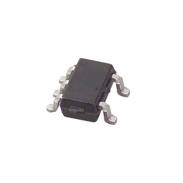
♦ Space-Saving 5-Pin SC70 or SOT23 Packages
Low-cost, low-dropout linear regulators can be designed
with the MAX8515A/MAX8515 and an external NPN transistor for cost-conscious applications that do not require
overcurrent, short-circuit, or overtemperature protection.
The MAX8515/MAX8515A are available in space-saving
5-pin SC70 and SOT23 packages and are specified over
the -40°C to +85°C extended temperature range. An evaluation kit is available to speed designs.
Applications
♦ MAX8515
0.6V ±1% Initial Accuracy at +25°C
0.6V ±1.8% Accuracy from -40°C to +85°C
♦ Sinks 20mA at 0.2V to 18V
♦ Input Voltage Range from 1.7V to 28V
♦ Directly Drives Optocouplers
♦ 0.2Ω Dynamic Output Impedance
Ordering Information
PART
TEMP RANGE
PIN-PACKAGE
MAX8515AEXK-T
-40°C to +85°C
5 SC70-5
MAX8515AEZK-T
-40°C to +85°C
5 Thin SOT23-5
MAX8515EXK-T
-40°C to +85°C
5 SC70-5
MAX8515EZK-T
-40°C to +85°C
5 Thin SOT23-5
Functional Diagram appears at end of data sheet.
Selector Guide appears at end of data sheet.
Isolated DC-to-DC Converters
Network, Telecom, and Cellular Base Station
Power Supplies
Typical Operating Circuit
Low-Dropout Linear Regulators
INPUT SUPPLY
INPUT
1.7V TO 28V 1.7V TO 18V
Shunt Regulator
Adjustable Voltage Reference
PRIMARY SIDE
PWM CONVERTER
CONTROL
VOLTAGE
Pin Configuration
TOP VIEW
IN
FB
5
MAX8515A
MAX8515
N SC7
-PI
2.0
m
OUT 3
4
IN
0
GND 2
5
mm
PGND 1
m x 2.1
MAX8515A
MAX8515
PGND
GND
OUT
FB
ISOLATED DC-DC
CONVERTER
OUTPUT
(DOWN TO 0.6V)
SC7O/THIN SOT23
________________________________________________________________ Maxim Integrated Products
For pricing, delivery, and ordering information, please contact Maxim/Dallas Direct! at
1-888-629-4642, or visit Maxim’s website at www.maxim-ic.com.
1
MAX8515A/MAX8515
General Description
The MAX8515A/MAX8515 shunt regulators simplify the
design of voltage regulation and overvoltage protection
(OVP) functions in high-accuracy isolated DC-to-DC converters with output voltages as low as 0.6V. The devices
have supply voltage and feedback inputs separated from
the output shunt stage, and can operate directly from the
DC-to-DC converter output stage when the output voltage
is 1.8V to 18V. Alternately, the MAX8515A/MAX8515 input
stage can be biased from an unregulated 1.7V to 28V
supply, independent of DC-to-DC converter output voltage. The MAX8515A/MAX8515 shunts 20mA when the
output voltage is as low as 0.2V.
�MAX8515A/MAX8515
Wide-Input 0.6V Shunt Regulators for
Isolated DC-to-DC Converters
ABSOLUTE MAXIMUM RATINGS
IN to GND ...............................................................-0.3V to +30V
OUT to GND ...........................................................-0.3V to +20V
FB to GND .................-0.3V to the lower of 5.5V and (VIN +0.3V)
PGND to GND .......................................................-0.3V to +0.3V
Continuous Power Dissipation (TA =+70°C)
5-Pin SC70 (derate 3.1mW/°C above +70°C) ...........246.9mW
5-Pin Thin SOT23 (derate 9.1mW/°C above +70°C) ....727mW
Operating Temperature Range ...........................-40°C to +85°C
Junction Temperature Range ............................-40°C to +150°C
Storage Temperature Range .............................-65°C to +150°C
Lead Temperature (soldering, 10s) .................................+300°C
Stresses beyond those listed under “Absolute Maximum Ratings” may cause permanent damage to the device. These are stress ratings only, and functional
operation of the device at these or any other conditions beyond those indicated in the operational sections of the specifications is not implied. Exposure to
absolute maximum rating conditions for extended periods may affect device reliability.
ELECTRICAL CHARACTERISTICS
(VIN = 3.3V, OUT = FB, IOUT = 5mA, TA = -40°C to +85°C, unless otherwise noted. Typical values are at TA = +25°C.) (Note 1)
PARAMETER
SYMBOL
CONDITIONS
MIN
TYP
MAX
UNITS
28
V
IN
IN Voltage Range
IN Supply Current
VIN
IIN
1.7
VIN = 2V to 28V
IOUT = 0.3mA
0.5
1
IOUT = 10mA
2.5
4
mA
FB
TA = +25°C
FB Threshold Accuracy
TA = 0°C to +85°C
TA = -40°C to +85°C
FB Load Regulation
FB Line Regulation
0.597
0.6
0.603
MAX8515E_K
0.594
0.6
0.606
MAX8515AE_K
0.595
0.6
0.605
MAX8515E_K
0.592
0.6
0.608
MAX8515AE_K
0.594
0.6
0.606
MAX8515E_K
0.589
0.6
0.608
IOUT = 1mA to 20mA
3.8
6
VIN = 2V to 28V
0.2
1
VIN = 1.7V to 28V
FB Output Voltage Regulation
FB Input Bias Current
MAX8515AE_K
1.5
VOUT = 0.2V to 18V, IOUT = 1mA
IFB(BIAS)
VIN = 28V
-0.1
V
mV
mV
0.2
1
mV
0.02
+0.1
µA
OUT
OUT Voltage Range
VOUT
0.2
Maximum Output Current
IOUT(MAX) VOUT = 0.2V, VIN = 2V, VFB = 0.63V
Output Leakage Current
IOUT(LEAK)
Dynamic Output Impedance
ZOUT
VIN = 28V, VOUT = 18V,
VFB = 0V
18
20
TA = +25°C
0.001
TA = +85°C
0.03
IOUT = 1mA to 20mA, f
很抱歉,暂时无法提供与“MAX8515EXK+TG002”相匹配的价格&库存,您可以联系我们找货
免费人工找货