19-0653; Rev 0; 11/06
KIT
ATION
EVALU
E
L
B
A
AVAIL
Complete Backup Management
IC for NiMH Batteries
The MAX8672 complete power manager for backup
batteries in smart devices offers feature-programmable
battery charging and main-system backup. The device
includes a charger for 1- or 2-cell NiMH backup batteries. A low-quiescent current synchronous-rectified
boost converter and LDO supply up to 20mA during
system backup. The BST output is internally set to regulate at 3.05V. The MAX8672 LDO is powered from the
boost converter output and is adjustable from 1.5V to
3.05V.
The MAX8672 features programmable charge current,
undervoltage lockout (UVLO), and maximum cell voltage. Charging is controlled by both a timer and thermistor monitor. Battery UVLO prevents excessive
battery discharge and keeps inactive-battery drain current below 50nA. In addition, both LDO and boost converter outputs block reverse current so that diodes are
not needed when connecting these outputs directly to
system supplies. The MAX8672 requires that a valid
system supply be present before system backup operation can occur.
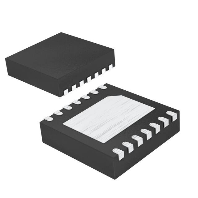
The MAX8672 is available in a 14-pin, 3mm x 3mm TDFN
package and is rated for -40°C to +85°C operation.
Features
o
o
o
o
o
o
o
o
o
o
Charges 1- or 2-Cell NiMH Backup Batteries
Programmable Charge Current
DC Trickle Charge Mode for Maximum Cell Life
Deep-Recovery Charge Restores Cells < 1V
Programmable Charge Timer
Programmable Charge-Voltage Limit and Battery
UVLO
Reverse Current Blocking on BATT, LDO, and
Boost—No Diodes Needed
No Battery Drain When Off (< 50nA)
Thermistor Sensing Disables Standard Charge
Battery Restart Charge Threshold Prevents
Overcharge
Ordering Information
PART
PIN-PACKAGE
MAX8672ETD+T
PKG CODE
14 TDFN-14 (3mm x 3mm)
T14334+2
The MAX8672 operates in the -40°C to +85°C extended
operating temperature range.
+Denotes lead-free package.
Typical Operating Circuit
Applications
PDA, Palmtop, and Wireless Handhelds
THRM
CT
Smart Cell Phones
MAX8672
Pin Configuration
2.7V TO 5.5V INPUT
IN
CHGV
CHGV
FBL
LDO
BST
LX
GND
TOP VIEW
THRM
DR
14
13
12
11
10
9
8
CHGI
TRKI
FBL
BATT
BACKUP BATTERY
CONNECTION
MAX8672
LDO
1.75V
BST
3.05V
5
6
7
IN
UV
4
DR
CHGI
3
BATT
2
TRKI
1
CT
UV
TDFN
(3mm x 3mm)
GND
LX
________________________________________________________________ Maxim Integrated Products
For pricing, delivery, and ordering information, please contact Maxim/Dallas Direct! at
1-888-629-4642, or visit Maxim’s website at www.maxim-ic.com.
1
MAX8672
General Description
�MAX8672
Complete Backup Management
IC for NiMH Batteries
ABSOLUTE MAXIMUM RATINGS
IN, BATT, BST, LDO, UV to GND ..........................-0.3V to +6.0V
FBL to GND ...............................................-0.3V to (VBST + 0.3V)
CT, CHGI, TRKI, CHGV, THRM,
DR to GND ...............................................-0.3V to (VIN + 0.3V)
ILX ..................................................................................0.9ARMS
Continuous Power Dissipation (TA = +70°C)
14-Pin, 3mm x 3mm TDFN
(derate 18.2 mW/°C above +70°C) .........................1454.5mW
Operating Temperature Range ...........................-40°C to +85°C
Junction Temperature ......................................................+150°C
Storage Temperature Range .............................-65°C to +150°C
Lead Temperature (soldering, 10s) .................................+300°C
Stresses beyond those listed under “Absolute Maximum Ratings” may cause permanent damage to the device. These are stress ratings only, and functional
operation of the device at these or any other conditions beyond those indicated in the operational sections of the specifications is not implied. Exposure to
absolute maximum rating conditions for extended periods may affect device reliability.
ELECTRICAL CHARACTERISTICS
(VIN = 3.6V, TA = -40°C to +85°C, CCT = 0.1µF, unless otherwise noted.) (Note 1)
PARAMETER
IN Voltage Range
IN Undervoltage Lockout Threshold
IN Supply Current
Internal Load Current on BST
(Note 2)
CONDITIONS
MIN
TYP
MAX
UNITS
2.45
40
117
5.5
2.60
100
170
V
V
µA
TA = -40°C to +50°C
91
125
µA
TA = -40°C to +85°C
91
150
2.7
2.20
VIN rising, hysteresis = 100mV (typ)
VBATT > VBATT(CHG)
VIN = 3.3V
VBST = 3.3V, no
BST or LDO load,
boost and LDO on
VIN = 0V
BATT Quiescent Supply
Current—Backup Mode
VBATT = 1.55V, VBST = 3.3V,
VIN = 0V, VBATT(CHG) = 1.5V
BATT Quiescent Supply Current—Charging
VBATT = 1.55V, VBST = 3.3V, VIN = 3.6V
BATT Leakage Current to IN
VBATT = 3.0V,
VIN = 0V
Total BATT Battery Leakage Current During
UVLO (BATT, LX, and DR Leakage)
VBATT = 0 to 3.0V
3
µA
3
µA
TA = +25oC
0.01
0.1
TA = +85oC
TA = -40°C to +50°C
0.07
5
50
TA = +85oC
50
µA
nA
CHARGER AND BATTERY
1mA ≤ IBATT(CHG) ≤ 20mA,
VIN - VBATT > 400mV
CHGI Current-Limit Accuracy
IBATT(CHG) = 1mA, VIN VBATT > 400mV
0.1mA ≤ IBATT(CHG) ≤ 1mA,
VIN - VBATT > 400mV
TA = -40oC to +85oC
-10
+10
TA = 0oC to +85oC
-10
+10
o
TA = -40 C to +85 C
-15
+15
TA = -40oC to +85oC
-20
+20
o
CHGI Bias Voltage
CHGI Resistor Range
600
IBATT(TRK) = 1mA
TRKI Current-Limit Accuracy
IBATT(TRK) = 0.1mA
5
1000
TA = -40oC to +85oC
-10
+10
TA = 0oC to +85oC
-10
+10
o
-15
+15
o
TA = -40 C to +85 C
%
mV
kΩ
%
DC Trickle-Current Programming Range
IBATT(TRK)
0.1
1
mA
Charge-Current Programming Range
IBATT(CHG)
0.1
20
mA
TRKI Bias Voltage
600
TRKI Resistor Range
Charger Dropout Voltage
2
100
VIN - VBATT where IBATT(CHG) falls by 10% of initial
value; VIN = 3.6V, IBATT(CHG) = 20mA
mV
1000
250
_______________________________________________________________________________________
kΩ
mV
�Complete Backup Management
IC for NiMH Batteries
(VIN = 3.6V, TA = -40°C to +85°C, CCT = 0.1µF, unless otherwise noted.) (Note 1)
PARAMETER
CHGV Output Current
CONDITIONS
MIN
VCHGV = 1V
Measured at BATT
o
TA = +25 C
VBATT(CHG) Voltage-Limit Accuracy
VBATT(TRK) to VBATT(CHG) Ratio
RCHGV = 28.7kΩ
MAX
13
CHGV Resistor Range
VBATT(CHG) Voltage-Limit Adjust Range
TYP
UNITS
µA
28.7
57.4
kΩ
1.50
3.00
V
-1
+1
TA = 0oC to +50oC
-1.25
+1.25
TA = -30oC to +85oC
-2.25
+2.25
%
Sets 1.41V when VCHGV = 1.5V, measured at BATT
0.926
0.940
0.954
—
VBATT(RSTRT) to VBATT(CHG) Ratio
Sets 1.225V when VCHGV = 1.5V, measured at BATT
0.799
0.816
0.832
—
VBATT(DR) to VBATT(CHG) Ratio
Sets 1.00V when VCHGV = 1.5V, measured at BATT; this
is the VBATT above which deep recovery (DR) turns off;
the falling threshold is typically 50mV below this
0.653
0.667
0.680
—
0.775
0.816
0.861
—
10
20
%
VDR Output Voltage to VBATT(CHG) Ratio Measured at BATT; no load on DR
DR Load Regulation
IDR = 0 to 10mA
o
TA = +25 C
20
TA = -40oC to +85oC
25
Charge-Timer Accuracy
Does not include
capacitor error
Timer Adjust Range
CHGI timer period, CCT = 0.047µF = 8h (480min)
Thermistor Hot-Trip Point
Thermistor Cold-Trip Point
2
Cold-Trip Thermistor Resistance
UV Output Current
min
o
44
45
46
o
C
o
-2
-1
0
o
C
o
C
RTHERM = 100kΩ at TA = +25 C, TA rising
RTHERM = 100kΩ at TA = +25 C, TA falling
Thermistor Temperature Hysteresis
Hot-Trip Thermistor Resistance
2000
%
2
TA rising
42.00
TA falling
43.71
45.42
48.15
TA falling
325.5
342.0
TA rising
302.0
VUV = 1V
4
358.6
kΩ
µA
UV Resistor Range
49.9
215
kΩ
UV Battery-Cutoff Programmable Range
0.8
3.5
V
-2
+2
-3.25
+3.25
1.5
3.05
UV Battery-Cutoff Accuracy
RUV = 49.9kΩ
TA = 0oC to +50oC
TA = -30oC to +85oC
%
LDO
LDO Output-Voltage Range
Using external resistors, no load
FBL Regulation Voltage
VBST = 3.3V, VLDO = 3.05V
LDO Output Current
(Note 3)
LDO Load Regulation
VBST = 3.3V, VLDO = 3.05V, ILDO = 1mA to 20mA
LDO Dropout Voltage
LDO Dropout Resistance
FBL Input Bias Current
1.275
V
20
mA
0.08
0.2
%/mA
VLDO = 2.5V, ILDO = 10mA
50
100
mV
VLDO = 2.5V
5
VFBL = 1.25V
1.225
1.25
V
TA = +25oC
3
TA = +85oC
15
Ω
50
nA
_______________________________________________________________________________________
3
MAX8672
ELECTRICAL CHARACTERISTICS (continued)
�ELECTRICAL CHARACTERISTICS (continued)
(VIN = 3.6V, TA = -40°C to +85°C, CCT = 0.1µF, unless otherwise noted.) (Note 1)
PARAMETER
CONDITIONS
MIN
TYP
MAX
UNITS
2.989
3.05
3.111
V
20
mA
600
mA
Ω
BOOST CONVERTER
BST Output Voltage
Boost Output Current
1-cell input (Note 3)
LX Current Limit
400
500
n-Channel On-Resistance
ILX = 200mA
0.4
1
p-Channel On-Resistance
ILX = -200mA
0.7
2
Ω
3.5
5
6.5
µs
5
20
35
mA
n-Channel Maximum On-Time
p-Channel Off-Current Threshold
Note 1: Parameters are 100% production tested at TA = +25°C. Limits over the operating temperature range are guaranteed by design.
Note 2: BATT current is higher due to boost ratio and efficiency.
Note 3: Total load from both BST and LDO cannot exceed 20mA.
Typical Operating Characteristics
(VIN = 3.6V, Circuit of Figure 6, TA = +25°C, unless otherwise noted.)
10
ICHG = 3mA
5
VBST = 3.3V,
VBATT(CHG) = 3V,
RDR = 549Ω,
VBATT RISING
10
ICHG = 3mA
5
ICHG = 200μA
0.25 0.50 0.75 1.00 1.25 1.50 1.75 2.00
0
0
0.5
1.0
2.5
3.0
0
3.5
0.5 1.0 1.5 2.0 2.5 3.0 3.5 4.0 4.5 5.0
BATTERY-CHARGE PROFILE
(2 NiMH CELLS)
ICHG = 3mA
5
ICHG = 200μA
0.5 1.0 1.5 2.0 2.5 3.0 3.5 4.0 4.5 5.0
INPUT VOLTAGE (V)
3.5
MAX8672 toc06
2.15
3.0
2.10
VBATT (V)
2.5
2.05
CHARGE
TERMINATION
AT VBATT(CHG)
2.0
1.5
1.0
2.00
VBATT = 2.4V,
VBST = 3.3V,
RCHGI = 49.9kΩ
0
4
2.0
CHARGE CURRENT (ICHG)
vs. TEMPERATURE
VBATT = 2.4V,
RCHGV = 57.6kΩ,
VBST = 3.3V
0
1.5
ICHG = 200μA
-5
2-CELL CHARGE CURRENT (ICHG)
vs. INPUT VOLTAGE (VIN)
20
-5
ICHG = 3mA
5
INPUT VOLTAGE (V)
ICHG = 20mA
10
10
BATTERY VOLTAGE (V)
25
15
VBATT = 1.2V,
RCHGV = 28.7kΩ,
VBST = 3.3V
15
BATTERY VOLTAGE (V)
CHARGE CURRENT (mA)
0
ICHG = 20mA
20
ICHG = 200μA
0
MAX8672 toc04
0
MAX8672 toc02
20
15
25
CHARGE CURRENT (mA)
VBST = 3.3V,
VBATT(CHG) = 1.5V,
RDR = 274Ω,
VBATT RISING
15
ICHG = 20mA
MAX8672 toc05
CHARGE CURRENT (mA)
20
25
CHARGE CURRENT (mA)
ICHG = 20mA
MAX8672 toc01
25
1-CELL CHARGE CURRENT (ICHG)
vs. INPUT VOLTAGE (VIN)
2-CELL CHARGE CURRENT (ICHG)
vs. BATTERY VOLTAGE (VBATT)
MAX8672 toc03
1-CELL CHARGE CURRENT (ICHG)
vs. BATTERY VOLTAGE (VBATT)
CHARGE CURRENT (mA)
MAX8672
Complete Backup Management
IC for NiMH Batteries
1.95
-40
-15
35
10
TEMPERATURE (°C)
60
85
TRICKLE
CHARGE
STARTS AT
VBATT(TRK)
VIN = 4V, VBST = 3.3V, R1 = 402kΩ,
R2 = 24.9kΩ, R3 = 165kΩ, R4 = R5 = 124kΩ,
R6 = 56kΩ, R7 = OPEN, R8 = SHORT,
R9 = 110kΩ, C1 = 0.047μF
0.5
0
0
60
120 180 240 300 360 420
TIME (min)
_______________________________________________________________________________________
480
�Complete Backup Management
IC for NiMH Batteries
VBATT = 1.2V
60
50
40
30
20
10
300
250
200
150
50
VIN = NOT CONNECTED
0
0.01
0.1
1
0
100
10
0.8
1.6
2.4
2.8
VBATT(CHG) =
1.5V
17.5
15
2.0
2.5
60
90
120
150
180
CT FREQUENCY vs. TEMPERATURE
18.0
17.5
CT FREQUENCY (Hz)
12.5
10.0
7.5
17.0
16.5
16.0
5.0
VIN = VBST = VLDO = 0V
VBATT = 0.9V
RCHGV = 28.7kΩ
2.5
0.0
1.0
30
15.0
RDR = 100Ω
3.0
-40
-15
BATTERY VOLTAGE (V)
10
35
60
15.5
CCT = 0.047μF, X7R, 10%
15.0
85
-40
-15
10
35
60
85
TEMPERATURE (°C)
TEMPERATURE (°C)
MAX BATT CHARGE VOLTAGE
vs. TEMPERATURE (1-CELL NiMH)
LIGHT-LOAD SWITCHING WAVEFORMS
MAX8672 toc14
MAX8672 toc13
1.55
MAX BATT CHARGE VOLTAGE (V)
0.5
2.9
0
MAX8672 toc11
BATT INPUT LEAKAGE CURRENT (nA)
MAX8672 toc10
5
VBATT = 2.4V
VBATT = 1.2V
BST LOAD CURRENT (mA)
20.0
VBATT(CHG) = 3.0V
3.0
3.2
BATT INPUT LEAKAGE CURRENT DURING UVLO
vs. TEMPERATURE
10
3.1
2.8
2.0
DR CURRENT (IDR)
vs. BATTERY VOLTAGE (VBATT)
15
0
1.2
BATT VOLTAGE (V)
20
0
ILDO ,IBST = 0A,
VIN = NOT CONNECTED,
BACKUP MODE
BST LOAD CURRENT (mA)
25
DR CURRENT (mA)
350
100
VIN = NOT CONNECTED
BST OUTPUT VOLTAGE (V)
400
MAX8672 toc09
450
BATT CURRENT (μA)
VBATT = 2.4V
70
3.2
MAX8672 toc08
90
EFFICIENCY (%)
500
MAX8672 toc07
100
80
BST OUTPUT VOLTAGE
vs. BST LOAD CURRENT
BATT INPUT CURRENT (WHILE BOOSTING)
vs. BATT VOLTAGE
MAX8672 toc12
BST EFFICIENCY
vs. BST LOAD CURRENT
1.53
3.05V
VBST
50mV/div
VLX
1V/div
1.51
1.49
0V
1.47
RCHGV = 28.7kΩ
1.45
-40
-15
10
35
60
85
ILX
200mA/div
IBST = 2mA
0A
10μs/div
TEMPERATURE (°C)
_______________________________________________________________________________________
5
MAX8672
Typical Operating Characteristics (continued)
(VIN = 3.6V, Circuit of Figure 6, TA = +25°C, unless otherwise noted.)
�Typical Operating Characteristics (continued)
(VIN = 3.6V, Circuit of Figure 6, TA = +25°C, unless otherwise noted.)
HEAVY-LOAD SWITCHING WAVEFORMS
BST LOAD TRANSIENT
MAX8672 toc15
MAX8672 toc16
3.05V
VBST
50mV/div
IBST
20mA/div
VLX
1V/div
0A
0V
0V
ILX
200mA/div
VBST
20mV/div
AC-COUPLED
IBST = 20mA
VBATT = 2.4V
0A
10μs/div
200μs/div
BST OUTPUT VOLTAGE
vs. LDO LOAD CURRENT
LDO LOAD TRANSIENT
VIN = NOT CONNECTED
MAX8672 toc17
MAX8672 toc18
3.2
BST OUTPUT VOLTAGE (V)
3.1
ILDO
20mA/div
0A
3.0
VLDO
10mV/div
AC-COUPLED
VBATT = 2.4V
VBATT = 1.2V
2.9
0V
VBATT = 2.4V
2.8
0
30
60
90
120
150
200μs/div
180
LDO LOAD CURRENT (mA)
BATTERY RIPPLE (VBATT_P-P)
vs. TEMPERATURE
BST RESPONSE TO LDO LOAD TRANSIENT
MAX8672 toc19
MAX8672 toc20
300
250
CBATT = 10μF
ILDO
0A
20mA/div
VBATT_P-P (mV)
MAX8672
Complete Backup Management
IC for NiMH Batteries
200
150
100
VBST
20mV/div
AC-COUPLED
0V
CBATT = 47μF
50
VBATT = 2.4V
200μs/div
0
-20 -15 -10 -5 0 5 10 15 20 25 30 35 40 45
TEMPERATURE (°C)
6
_______________________________________________________________________________________
�Complete Backup Management
IC for NiMH Batteries
PIN
NAME
1
CT
2
CHGI
Programming Input for the Standard Charge-Current Rate. Connect a resistor (RCHGI) from CHGI to GND to
program the standard charge current from 100µA to 20mA.
3
TRKI
Programming Input for the DC Trickle-Charge Rate. Connect a resistor from TRKI to GND to program the
trickle-charge current.
4
BATT
Backup-Battery Connection. The backup battery charges from IN but does not allow reverse current to IN
when VIN < VBATT. BATT input current is less than 0.1µA when VBATT is below the UV threshold.
5
IN
Power Input. Range is 2.7V to 5.5V.
DR
Programming Input for Deep-Recovery Threshold. The DR output adds charge current when VBATT is below the
VBATT(DR) threshold (and THRM is valid) by biasing an external resistor connected from DR to BATT. The DR
output voltage, VDR, is 0.816 times the VBATT(CHG) limit set by VCHGV (VDR = 1.224V for a 1.5V VBATT(CHG)). The
DR current is sourced in addition to the standard charge current set by RCHGI.
7
UV
Programming Input for the BATT Undervoltage Lockout (UVLO), VBATT(UV). The UVLO threshold is
programmed by connecting a resistor from UV to GND. The backup LDO and boost converter cannot start
after UVLO occurs, or on power-up, until a valid VIN and VBST are applied. VBATT(UV) is programmable from
VBATT = 0.8V to 3.5V. An open circuit at UV disables the boost and LDO and interrupts battery drain. UVLO
also latches off backup circuitry to minimize battery drain.
8
GND
9
LX
10
BST
11
LDO
LDO Output. Programmable from 1.5V to 3.05V. LDO has reverse current blocking.
FBL
Programming Input for the LDO Output Voltage. Connect FBL to the center of a resistor-divider connected
between LDO and GND. The FBL threshold is 1.25V.
6
12
13
CHGV
FUNCTION
Programming Input for Charge Timer. Connect a capacitor from CT to GND to program the charge timer
(range: 2min to 2000min, nominally programmed to 8h = 480min with CCT = 0.047µF).
Ground
Boost Converter Switch Node. Connect the boost inductor from LX to BATT.
Boost Converter Output. BST has reverse current blocking when VBST is higher than VIN or VBATT. The
MAX8672 operates with VBST down to 2.35V. The BST output is factory preset for 3.05V for use with 3.3V
systems. Other voltages are available on request.
Programming Input for the Charge Voltage Limit (VBATT(CHG)). Also programs the trickle threshold
(VBATT(TRK)), standard charge-restart voltage (VBATT(RSTRT)), DR threshold (VBATT(DR)), and the DR output
voltage (VDR). For NiMH, program 1.5V VBATT(CHG) per cell, so that the max possible voltage is 1.55V per cell
with tolerances. VBATT(CHG) is programmable from 1.5V to 3.0V by connecting a resistor from CHGV to GND.
When the battery voltage rises to VBATT(CHG), standard charging stops. When the battery voltage falls to
VBATT(TRK), trickle charge begins. Standard charge does not resume until the battery voltage falls to
VBATT(RSTRT).
14
—
THRM
External Thermistor Monitor Connection. Connect an NTC (100kΩ at TA = +25°C) thermistor for -1°C and
+45°C charging cutoff. Only trickle charging is allowed outside the temperature limits. These temperature
thresholds are programmable by adding series and parallel resistors to the external thermistor. See Table 1.
EP
Exposed Pad. Connect to GND but do not rely on EP for ground functions. This pad is internally connected to
ground through a soft connect, meaning there is no internal metal or bond wire physically connecting the
exposed pad to the GND pin. Connecting the exposed pad to ground does not remove the requirement for a
good ground connection to the appropriate pins. For good thermal dissipation, the exposed pad must be
soldered to the power ground plane.
_______________________________________________________________________________________
7
MAX8672
Pin Description
�MAX8672
Complete Backup Management
IC for NiMH Batteries
Detailed Description
100kΩ
THRM
REF
OK
HOT
OK
COLD
CT
CHGV
2X
VCHG
COMP
TIMER
+ LOGIC
VTRK
COMP
IN
VRSTRT
COMP
DR
A=2
CHGI
VDR
COMP
TRKI
VBATT / 2
A=1
R
BATT
R
LDO
FBL
OFF
UV
MAX8672
3.05V
HYST*
AND
LDO
AND LO
BST
LOW IQ
BOOST
CONVERTER
The MAX8672 has three states:
• System Active/Charging. With a valid VIN (greater
than 2.7V and also greater than VBATT), and a valid
V BST (greater than 2.35V), the battery charges.
LDO and BST are active and available for system
backup. Charging and system backup are independent functions.
•
Backup. When the system supply voltages have
fallen below the programmed output voltage, BST
and LDO maintain their output voltages and are
sourced by the battery. Under these conditions,
battery charging has ceased, but this is not a
requirement for the backup state.
•
Off. When the battery voltage has fallen below the
UVLO threshold (VBATT(UV)) and VIN is not valid,
the IC turns off and all outputs are latched off. If
VBATT recovers to above VBATT(UV), charging does
not resume until both a valid VIN and VBST are present. Negligible battery current (less than 50nA
leakage) is drawn in this state.
HYST*: 0.85V
HYSTERESIS,
COMPARATOR
HI AT 3.05V,
LO AT 2.2V
AND HI
LX
The MAX8672 is a compact IC for managing backupbattery charging and utilization in PDAs and other smart
handheld devices. The IC contains three major blocks:
a charger for 1 or 2 NiMH coin cells; a small, very-lowquiescent current step-up DC-DC converter that generates a boosted backup supply; and an LDO that can
supply a 2nd backup voltage to an additional system
block (typically low-voltage RAM).
The MAX8672 does not have a logic control signal for
activating backup. The main system supplies are
directly connected to the BST and LDO outputs, where
LDO and BST are programmed to regulate just below
system supply voltages. When system supply voltages
exceed the programmed BST and LDO output voltage,
BST and LDO are pulled up by the system supplies
and do not sink current (BST sinks 80µA for chip operation). When the system supplies fall below the programmed output voltage, BST and LDO operate to
maintain system voltages at the programmed values.
The LDO and boost converter do not operate any differently in the system’s running (and charging) state than
they do in the backup state. The LDO and BST error
amplifiers constantly monitor their outputs in both cases.
PFM
Figure 1. MAX8672 Functional Block Diagram
8
_______________________________________________________________________________________
�Complete Backup Management
IC for NiMH Batteries
CHARGE
TIMER
EXPIRES
limit is achieved. Once standard charge or trickle charge
is terminated by the VBATT(CHG) limit, charging ceases.
Subsequently, if VBATT falls to the VBATT(TRK) threshold,
trickle charge is activated. VBATT then rises and the
charging cycle continues. The charger does not enter
standard charge again until the battery falls to the
VBATT(RSTRT) threshold. When the VBATT(RSTRT) threshold is reached, standard charge begins and the charge
timer is reset.
Standard charge is also interrupted if the external thermistor temperature sensed at THRM is out of range.
When THRM senses a too-hot or too-cold condition during standard charge, the timer pauses and the charger
enters trickle charge.
NO
CHARGE
1.5V
VBATT(CHG)
1.41V
VBATT(TRK)
NO
CHARGE
TRICKLE
STANDARD
CHARGE
1.225V
VBATT(RSTRT)
1.5V
NO
CHARGE
VBATT(CHG)
TRICKLE
1.41V
VBATT(TRK)
NO
CHARGE
TRICKLE
STANDARD
CHARGE
1.225V
VBATT(RSTRT)
Figure 2. Typical Charge-Current Profiles for 1-Cell Battery
_______________________________________________________________________________________
9
MAX8672
Charger
The MAX8672 charger is a comparator-controlled current source with both current and voltage limits programmed by external resistors. Typical charge profiles
for a 1-cell NiMH battery are shown in Figure 2 and
explained below.
When power is applied at IN and BST, the MAX8672
charges the battery at the standard charge current programmed by a resistor connected between CHGI and
GND. The MAX8672 remains in standard charge until the
charge timer (programmed by CCT) times out, the battery
rises to the VBATT(CHG) limit, or the charge is interrupted
by a temperature-range violation. If standard charge is
terminated by the charge timer, trickle charge mode
begins and continues without timing until the VBATT(CHG)
�MAX8672
Complete Backup Management
IC for NiMH Batteries
A valid voltage is required on both IN and BST for standard and trickle charging. Once charging begins, if
VIN becomes invalid, charging stops, but the timer is
paused since the backup circuitry is supplying BST. If
VBST falls below 2.2V, the timer resets.
If the thermistor hot- or cold-temperature threshold is
violated, the charge timer pauses and only trickle
charging is allowed. When THRM recovers, the
MAX8672 goes to RUN instead of reentering the charge
mode. This is done to reevaluate the battery state when
the temperature returns to the normal operating range.
The charge timer is not reset when returning to the
RUN state.
Additionally, if VIN is interrupted during standard charge,
and the battery voltage is greater than VBATT(RSTRT), the
timer pauses until power is reapplied. If the battery voltage falls below VBATT(RSTRT), the timer resets. See the
charger state diagram in Figure 3 for more details on
charger operation.
Trickle charge occurs whenever standard charge is
interrupted by timeout, when VBATT falls to VBATT(TRK),
or when THRM senses an out-of-temperature-range
condition. Trickle charge has the same voltage limit as
standard charge and cannot drive the battery above
VBATT(CHG).
VBST
NOT OK
VBST
NOT OK
ANY
STATE
OFF
(RESET TIMER)
VBST OK
VIN NOT OK
AND
VBST OK
VIN NOT OK
AND VBST OK
ANY STATE EXCEPT
TRICKLE CHARGE AND
NO CHARGE
STAND BY
(TIMER PAUSED)
VIN NOT OK AND
VBST OK
(2-CELL, VCHG > 2.1V)
VIN OK
VBATT > VBATT(RSTRT)
RESET
TIMER
RUN
T > COLD
AND
T < HOT
COLD/HOT
TRICKLE
(TIMER PAUSED)
VBATT < VBATT(DR) - 50mV
RESET TIMER
COMPLETE
VBATT < VBATT(RSTRT)
VBATT > VBATT(DR)
STANDARD
CHARGE
DEEPRECOVERY
CHARGE
VBATT < VBATT(DR) - 50mV
TIMER
COMPLETE
VBATT > VBATT(CHG)
VBATT < VBATT(TRK)
TRICKLE
CHARGE
VBATT > VBATT(CHG)
T < COLD
AND
T > HOT
T < COLD
OR
T > HOT
VIN NOT OK AND
VBST OK
(1-CELL,
VCHG < 2.1V)
VBATT > VBATT(CHG)
NO CHARGE
AND
FORCE TIMER
COMPLETE
Figure 3. Charger State Diagram
10
______________________________________________________________________________________
�Complete Backup Management
IC for NiMH Batteries
or when THRM senses an out-of-temperature-range
condition. Trickle charge has the same voltage limit as
standard charge.
The trickle current is programmed from 100µA to 1mA
by connecting a resistor (R TRKI) from TRKI to GND
(Figure 4). After selecting the battery trickle charge current (IBATT(TRK)) for the application, RTRKI is determined by the following equation:
RTRKI (kΩ) =
100
IBATT(TRK)(mA)
R8
RCHGV =
VBATT(CHG)
C1
(CCT)
52265
.
× 10−6
(Note that the voltage at CHGV is VBATT(CHG) / 4.)
The other voltage thresholds associated with the charging cycle (Figure 2) are dependent upon the selection
of VBATT(CHG) as follows:
Falling battery threshold to begin trickle charge
(VBATT(TRK)):
VBATT(TRK) = 0.94 × VBATT(CHG)
Rising battery threshold to exit deep-recovery charge
(VBATT(DR)):
VBATT(DR) = 0.667 × VBATT(CHG)
Standard charging of the battery occurs when the
MAX8672 is first turned on, or when the battery is discharged below the VBATT(RSTRT) threshold. Standard
charge ceases when the VBATT(CHG) limit is reached.
The standard charge current (I BATT(CHG) ) is programmed from 0.1mA to 20mA by connecting a resistor
(RCHGI) from CHGI to GND (Figure 4). The valid range
of RCHGI is 5kΩ to 1MΩ. Once the value of standard
charge current (I BATT(CHG) ) has been chosen, the
required RCHGI is determined by the following equation:
RCHGI (kΩ) =
100
IBATT(CHG)(mA)
Trickle Charge
Trickle charge occurs whenever standard charge is
interrupted by timeout, when VBATT falls to VBATT(TRK),
TH1
100kΩ
AT +25°C
MAX8672
2.7V TO 5.5V INPUT
C2
(CIN)
IN
CHGV
R6
(RCHGV)
DR
C6
(CDR)
CHGI
TRKI
R1
(RDR)
R2
(RCHGI)
R4
FBL
R3
(RTRKI)
R5
Falling battery threshold to restart standard charge
(VBATT(RSTRT)):
VBATT(RSTRT) = 0.816 × VBATT(CHG)
THRM
CT
BATT
BACKUP
BATTERY
LDO
C3
(CBATT)
C5
(CLDO)
UV
L1
R9
(RUV)
BST
GND
C4
(CBST)
LX
Figure 4. External Component Diagram
Deep-Recovery Charge
The MAX8672 includes a circuit to bring up deep discharged NiMH cells. When power is first applied to IN,
if the battery voltage is less than the battery deeprecovery threshold, VBATT(DR), DR connects an internally regulated voltage to an external resistor that
sources extra current into the battery. The DR currentlimiting resistor is typically selected for a 0.5C charge
rate when the cell voltage is 0V. When DR is on, both
the standard charge current and the DR current charge
the battery. When the cell voltage reaches VBATT(DR),
DR current is turned off and standard charging begins.
______________________________________________________________________________________
11
MAX8672
Charger Voltage and
Standard Charge-Current Limits
The MAX8672 charger is a comparator-controlled current source with both current and voltage limits programmed by external resistors.
The maximum battery charge-voltage limit (VBATT(CHG))
is programmed by connecting a resistor (RCHGV) from
CHGV to GND (Figure 4). The range for the charging
voltage limit is 1.5V to 3.0V. For NiMH batteries,
VBATT(CHG) is typically selected for a 1.5V max charge
per cell. After selecting VBATT(CHG) for the intended
application, the required RCHGV is determined by the
following equation:
�MAX8672
Complete Backup Management
IC for NiMH Batteries
DR charging is allowed only when the THRM temperature is within hot and cold limits. The rising battery-voltage threshold for DR (V BATT(DR) ) is given by the
following equation:
VBATT(DR) = 0.667 × VBATT(CHG)
The DR output voltage is:
VDR = 0.816 × VBATT(CHG)
Thermistor Monitor
The thermistor monitor suspends standard charging
(and pauses the standard charge timer) when the thermistor temperature moves above +45°C or below -1°C.
The thermistor must be an NTC type with a nominal
+25°C resistance of 100kΩ.
The temperature trip thresholds are adjusted by adding
external resistors in series and in parallel with the thermistor. For the specified thermistor, the resistors values
are shown in Table 1.
Table 1. Series/Parallel Resistors for
Different Thermistor Thresholds (β)
SERIES R
(kΩ)
PARALLEL R
(MΩ)
HOT TEMP
(OC)
COLD TEMP
(OC)
0
None
45
-1
7.5
None
50
-0.6
13.7
None
55
-0.3
18.7
None
60
0
18.8
6.8
59.9
-1
22.7
None
65
0
23
5.6
65
-1
8.6
1.7
50
Note: With 100kΩ thermistors at +25°C, β = 3977.
-5
Charge Timer
The MAX8672 includes a charge timer that is programmable from 2min to 2000min. Timer duration is programmed by a capacitor, CCT, connected from CT to
GND (Figure 4). The charge-timer duration (tCHG) is
determined by the equation:
t CHG (minutes) = 10195 × CCT (μF)
Boost DC-DC Converter
The MAX8672 contains a low-current synchronous-rectified boost converter that can supply up to 20mA. The
boost converter’s preset output voltage is 3.05V,
intended for backing up a 3.3V supply. Preset output
voltages can be obtained from the factory on request.
Generally, the output voltage is programmed to be just
12
below the minimum tolerance for the main supply.
When the main supply voltage drops below its specified level, the step-up converter begins regulating as
long as the load is 20mA or less. The MAX8672 blocks
reverse current flow if VBST is higher than VBATT.
The MAX8672 typical application expects that a valid
system voltage is connected to BST and IN before
backup operations are required. The boost DC-DC
converter is able to supply a system load (up to 20mA)
when the main power source falls below the BST preset
voltage, but the IC cannot start up the BST output with
just the backup battery alone. BST must initially be
powered by the external system in order for the boost
converter to start. Then, if the system voltage falls
below the BST preset voltage, the boost converter can
supply the load. If necessary, this limitation can be
overcome for some applications by connecting a diode
from IN to BST, so that BST is immediately powered
from IN.
When VBATT is less than VBST, and VBST is not externally pulled above 3.05V by the main system supply,
the boost converter runs as needed to maintain VBST at
3.05V. If, during normal active/charging mode operation, VBATT rises above the main system voltage that is
connected to BST, current may flow from the battery to
the main system supply, even though no backup operation is expected. For example, in a 2-cell system, if
VBATT is 3.2V and the system supply is holding BST at
3.1V, then the backup battery drains into the system
supply. The boost synchronous rectifier pMOS contains
a body diode that is switched to prevent unwanted current flow (see the BATT-BST Current Flow section).
Since the normal maximum charge limit (VBATT(CHG))
for 2 NiMH cells is usually set to 3.0V (for a 3.1V max),
and a 3.3V system supply less a 5% tolerance is
3.135V, VBATT does not exceed VBST during normal
system operation, resulting in no backup current flow.
However, for other BATT or BST voltages where unwanted backup current flow may occur, it can be prevented
by connecting a diode in series with the boost inductor
to reduce the voltage at BST. The diode may be a
Schottky or silicon signal diode, depending on how
much voltage needs to be dropped.
Boost Output Capacitor Selection
Choose output capacitors to supply output peak currents with acceptable voltage ripple. Low equivalent
series resistance (ESR) capacitors are recommended.
Ceramic capacitors have the lowest ESR, but low-ESR
tantalum or polymer capacitors offer a good balance
between cost and performance.
______________________________________________________________________________________
�Complete Backup Management
IC for NiMH Batteries
VRIPPLE = VRIPPLE(C) + VRIPPLE(ESR)
VRIPPLE(ESR) = IPEAK × RESR
VRIPPLE(C) =
⎞
1⎛
L
2
⎜
⎟ IPEAK
2 ⎝ (VBST − VBATT ) × CBST ⎠
where IPEAK is the peak inductor current (see the Boost
Inductor Selection section). Since ESR is usually very
small in ceramic capacitors, the output ripple is typically dominated by VRIPPLE(C).
Capacitance and ESR variation with temperature
should be considered for best performance in applications with wide operating-temperature ranges.
Boost Inductor Selection
The control scheme of the MAX8672 permits flexibility
in choosing an inductor. A 4.7µH inductor performs well
in most applications.
For maximum output current, choose the inductor value
so that the controller reaches the current limit before
the maximum on-time is reached:
L<
VBATT × t ON(MAX)
ILIM
where tON(MAX) is typically 5µs, and the current limit (ILIM)
is typically 500mA (see the Electrical Characteristics).
For larger inductor values, determine the peak inductor
current (IPEAK) by:
IPEAK =
LDO
For backup designs that require two different backup
voltages, the MAX8672 includes a small LDO, which is
powered from BST. This LDO can supply up to 20mA.
Generally, the output voltage is programmed to be just
below the minimum tolerance for the main supply.
When the main supply voltage drops below its specified level, the LDO begins regulating.
The LDO output voltage is adjustable from 1.5V to 3.05V
using external resistors (R4 and R5 in Figure 4). Since
the FBL input bias current is 50nA (max), select feedback resistor R4 in the 100kΩ to 1MΩ range. After
choosing R4, calculate R5 as follows:
⎡V
⎤
R5 = R4⎢ LDO − 1⎥
⎣ VFBL
⎦
where VFBL = 1.25V.
Backup-Battery Bypass
Capacitor Selection
The MAX8672 boost converter draws 500mA short-term
inductor-charging current peaks from the battery when
the boost converter operates. Small coin cells that are
commonly used for backup often exhibit high output
impedance that varies over temperature. For this reason, the backup battery must be bypassed with a highquality ceramic capacitor with X7R, X5R, or better
dielectric (CBATT, Figure 4). Typical values are between
10µF and 47µF. Note that high battery ripple can prematurely trigger the UVLO comparator and shut down
the boost circuit before the battery is fully discharged.
If this is a concern with the selected battery, the UV
threshold may be lowered, in addition to using a larger
battery bypass capacitance, to accommodate the
short-term battery-voltage dip due to ripple. See the
Battery Ripple vs. Temperature graph in the Typical
Operating Characteristics section.
VBATT × t ON(MAX)
L
______________________________________________________________________________________
13
MAX8672
Output-voltage ripple has two components: variations
in the charge stored in the output capacitor (CBST) with
each BST pulse, and the voltage drop across the
capacitor’s ESR due to the current flow into and out of
the capacitor. The equations for approximating outputvoltage ripple are:
�MAX8672
Complete Backup Management
IC for NiMH Batteries
BACKUP READY*
(BOOST AND LDO ENABLED)
VIN > 2.45V
AND
VBST > 3.05V
AND
VBATT > VBATT(UV)
VBATT < VBATT(UV)
BATT UVLO
(BOOST AND LDO OFF)
*NOTE: BACKUP READY DOES NOT MEAN THAT THE BOOST AND LDO ARE OPERATING.
WHEN THE BST AND LDO OUTPUTS ARE ENABLED; THEY STILL ONLY OPERATE IF
NEEDED WHEN THE SYSTEM FAILS TO HOLD UP THE SUPPLIES.
Figure 5. Backup and BATT UVLO State Diagram
BATT Undervoltage Lockout
When the backup battery discharges to a programmed
threshold, VBATT(UV), BATT UVLO is engaged. As a
result, the MAX8672 backup functions (BST and LDO)
shut down, and a small current (less than 50nA) is
drawn from BATT. During BATT UVLO, charge functions still remain active to recharge the battery. Once
BATT UVLO occurs, the backup boost converter and
LDO do not reactivate until VBST rises above 3.05V and
VIN rises above 2.45V (typ). Even if BATT recovers, the
backup functions do not activate until a valid VIN and
VBST have been present. See the Backup and BATT
UVLO State Diagram (Figure 5).
The BATT UVLO threshold (VBATT(UV)) is programmed by
connecting a resistor (RUV) from UV to GND (Figure 4).
For NiMH cells, the UVLO threshold is typically programmed to 0.8V per cell. Once the UVLO threshold
value is determined, RUV is calculated from the following
equation:
VBATT(UV)
RUV =
16 × 10−6
14
Note: In order for BATT current to remain below 50nA
during BATT UVLO, VBST must fall below 0.5V. If VBST
is held up by another source during UVLO, or if VBST is
higher than 0.5V, BATT input current during BATT
UVLO is typically 500nA. Typically, VBST falls to 0V in
most situations. If minimum battery drain during BATT
UVLO is critical, then an external pulldown resistor connected between BST and GND may be needed to discharge the BST output.
The 500nA BATT drain during UVLO is necessary when
VBST is > 0.5V because a comparator must be kept
active in order to detect the higher of VBATT or VBST.
This comparator switches the body diode of the internal
FET connecting these outputs to ensure that current flow
is blocked. When VBST falls to approximately 0.5V, the
comparator is shut off, and the FET body is connected to
block current flowing from BATT to BST.
BATT-BST Current Flow
The MAX8672 synchronous rectifier pMOS contains an
internal body diode connected between BATT and
BST. This diode switches to prevent undesired current
flow between these pins. Upon startup, the body diode
points to the greater of VBATT or VBST, until VBST rises
above 3.05V (at least once). Then the body diode
switches to point to BST. The body diode points from
BATT to BST until V BST falls below 2.2V. When this
occurs, the body diode switches to point to the greater
of VBATT or VBST.
If VBATT exceeds VBST by a few hundred millivolts or
more, the body diode is forward biased and current
flows from BATT to BST. This is the typical case for a
boost converter when the input exceeds the output.
When backing up, this typically is not a problem since it
is expected that battery current powers the system.
When not in backup mode (system power is up and is
pulling VBST over 3.05V), current can flow from BATT to
BST if VBATT exceeds VBST by enough to forward bias the
diode. With two NiMH cells, VBATT charges to 3.0V nominal (3.1V max), so with VBST pulled to more than 3.05V by
the system, there is not enough voltage difference to
cause significant current to flow from BATT to BST.
______________________________________________________________________________________
�Complete Backup Management
IC for NiMH Batteries
R8
7.5kΩ
CT
Typical Application Circuit
Figure 6 displays the MAX8672 typical application circuit
for 2-cell NiMH applications. Corresponding to the
requirements for 2-cell NiMH batteries, maximum charge
voltage is programmed for 3.0V and the UVLO threshold
is set to 1.6V. The LDO output voltage is 1.75V. Standard
charge provides 2mA of standard charge current, while
trickle charge is programmed to provide 500µA of trickle
charge current. A 7.5kΩ resistor is connected in series
with the thermistor to program a hot temperature threshold of +50°C and a cold temperature threshold of -0.6°C.
C1
0.047μF
2.7V TO 5.5V INPUT
THRM
TH1
100kΩ
AT +25°C
IN
C2
0.1μF
DR
C6
0.22μF
R1
100Ω
CHGV
CHGI
TRKI
R2
50kΩ
R3
200kΩ
R6
57.6kΩ
R4
250kΩ
MAX8672
Layout Guidelines
Careful PCB layout is important for minimizing ground
bounce and noise. Ensure that C2 (IN input capacitor),
C3 (BATT input capacitor), C4 (BST bypass capacitor),
and C5 (LDO output capacitor) are placed as close as
possible to the IC. Avoid using vias to connect C3 or
C4 to their respective pins or GND. C3 and C4 grounds
should be located next to each other, and this connection can then be used as the star ground point. All other
grounds should connect to the star ground. Connect
EP to the bottom layer ground plane, and then connect
the ground plane to the star ground. Vias on the inductor path are acceptable, if necessary. IN, BATT, BST,
and LDO traces should be as wide as possible to minimize inductance. Refer to the MAX8672 evaluation kit
for a PCB layout example.
MAX8672
Applications Information
FBL
BATT
R5
100kΩ
C3
47μF
2-CELL
NiMH
1.75V
LDO
UV
L1
4.7μH
R9
100kΩ
C5
0.47μF
3.05V
BST
GND
C4
22μF
LX
Figure 6. Typical Application Circuit for the MAX8672 Using a
2-Cell NiMH
Chip Information
PROCESS: BiCMOS
______________________________________________________________________________________
15
�Package Information
(The package drawing(s) in this data sheet may not reflect the most current specifications. For the latest package outline information
go to www.maxim-ic.com/packages.)
6, 8, &10L, DFN THIN.EPS
MAX8672
Complete Backup Management
IC for NiMH Batteries
PACKAGE OUTLINE, 6,8,10 & 14L,
TDFN, EXPOSED PAD, 3x3x0.80 mm
21-0137
16
______________________________________________________________________________________
H
1
2
�Complete Backup Management
IC for NiMH Batteries
COMMON DIMENSIONS
PACKAGE VARIATIONS
SYMBOL
MIN.
MAX.
PKG. CODE
N
D2
E2
e
JEDEC SPEC
b
A
0.70
0.80
T633-1
6
1.50±0.10
2.30±0.10
0.95 BSC
MO229 / WEEA
0.40±0.05
1.90 REF
D
2.90
3.10
T633-2
6
1.50±0.10
2.30±0.10
0.95 BSC
MO229 / WEEA
0.40±0.05
1.90 REF
[(N/2)-1] x e
E
2.90
3.10
T833-1
8
1.50±0.10
2.30±0.10
0.65 BSC
MO229 / WEEC
0.30±0.05
1.95 REF
A1
0.00
0.05
T833-2
8
1.50±0.10
2.30±0.10
0.65 BSC
MO229 / WEEC
0.30±0.05
1.95 REF
L
0.20
0.40
T833-3
8
1.50±0.10
2.30±0.10
0.65 BSC
MO229 / WEEC
0.30±0.05
1.95 REF
T1033-1
10
1.50±0.10
2.30±0.10
0.50 BSC
MO229 / WEED-3
0.25±0.05
2.00 REF
k
0.25 MIN.
A2
0.20 REF.
T1033-2
10
1.50±0.10
2.30±0.10
0.50 BSC
MO229 / WEED-3
0.25±0.05
2.00 REF
T1433-1
14
1.70±0.10
2.30±0.10
0.40 BSC
----
0.20±0.05
2.40 REF
T1433-2
14
1.70±0.10
2.30±0.10
0.40 BSC
----
0.20±0.05
2.40 REF
PACKAGE OUTLINE, 6,8,10 & 14L,
TDFN, EXPOSED PAD, 3x3x0.80 mm
-DRAWING NOT TO SCALE-
21-0137
H
2
2
Maxim cannot assume responsibility for use of any circuitry other than circuitry entirely embodied in a Maxim product. No circuit patent licenses are
implied. Maxim reserves the right to change the circuitry and specifications without notice at any time.
Maxim Integrated Products, 120 San Gabriel Drive, Sunnyvale, CA 94086 408-737-7600 ____________________ 17
© 2006 Maxim Integrated Products
is a registered trademark of Maxim Integrated Products, Inc.
MAX8672
Package Information (continued)
(The package drawing(s) in this data sheet may not reflect the most current specifications. For the latest package outline information
go to www.maxim-ic.com/packages.)
�