EVALUATION KIT AVAILABLE
High-Efficiency, White LED
Step-Up Converter with I2C
Interface in 2mm x 2mm WLP
MAX8831
General Description
Benefits and Features
The MAX8831 integrates a 60mA, 28V PWM DC-DC
step-up converter with five low-dropout LED current
regulators for display and keypad backlighting in cell
phones, PDAs, and other portable devices. The IC provides up to 90% efficiency over the entire input voltage
range of 2.7V to 5.5V. The step-up converter operates
at a fixed 2MHz switching frequency, enabling the use
of very small external components to achieve a compact circuit area. For improved efficiency, the step-up
converter automatically transitions to pulse-skipping
mode at light loads.
Each of the five current regulators accommodates up to
9 series LEDs (depending on LED string forward voltage), and is independently programmed using an I2C
interface. Two of the current regulators (LED1, LED2)
are intended to support display backlight functions and
are programmable up to 25mA using a 128-step logarithmic dimming scheme. The other three regulators
(LED3, LED4, LED5) are suitable for keyboard backlight
functions or for driving signal indicators, and are programmable up to 5mA using a 32-step logarithmic dimming scheme. The low-current regulators (LED3, LED4,
LED5) can be operated from the step-up converter or
from a separate low-voltage source.
The I2C interface controls all operational aspects of the
current regulators, including: on/off state, LED current,
ramp-up/ramp-down timers, and blink rate timers
(LED3, LED4, LED5). The MAX8831 write/read addresses are factory programmed at 0x9A/0x9B (contact the
factory for other address options).
The MAX8831 features open/short LED fault detection,
output overvoltage protection, thermal shutdown, and
open-circuit Schottky diode detection, with the status of
each fault monitored continually for readback through
the I2C interface.
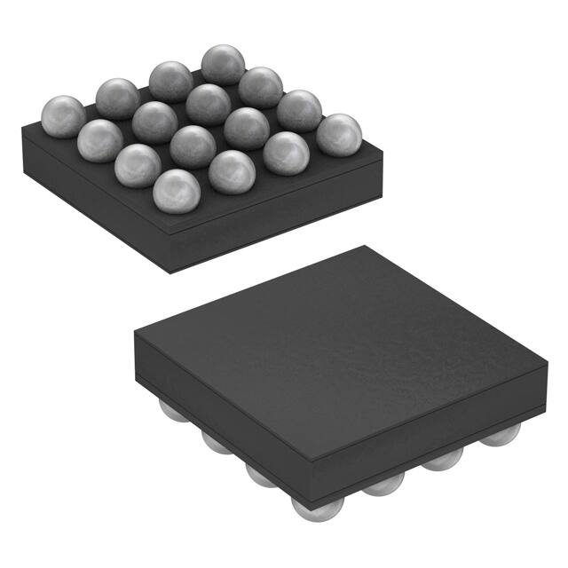
The MAX8831 is available in a tiny 2mm x 2mm, 16-bump
WLP package.
• Highly Integrated 28V Step-Up DC-DC Converter with
•
•
•
•
•
Programmable Functionality Lowers System Cost
• Integrated NMOS Power Switch
Two 25mA Regulators for Display Backlighting
• I2C-Programmable 50µA to 25.25mA Output Current
• 128-Step Logarithmic Dimming
• Individually Programmable Ramp (Up/Down) Timers
• Low Dropout (200mV max)
Three 5mA Current Regulators for Keypad Lighting
with I2C-Programmable 50µA to 5.0mA Output Current
• 32-Step Logarithmic Dimming
• Individually Programmable Ramp (Up/Down) Timers
• Individual Blink Rate and Duty Cycle Timers
• Low Dropout (150mV max)
• I2C Programmable Compatible with 1.8V Logic
Protection Features Increase Reliability
• Open/Short LED and Open-Circuit Diode Detection
• Thermal-Shutdown and Output Overvoltage
Protection
High Efficiency and Low Shutdown Current Extend
Battery Life
• > 90% Efficiency
• Pulse Skipping for Improved Light-Load Efficiency
• Ultra-Low 0.1µA Shutdown Current
Small Solution Size Saves Board Space
• Tiny 2mm x 2mm, 16-Bump WLP Package
• 2MHz Switching Frequency Allows Use of Tiny
External Components
Ordering Information
PART
MAX8831EWE+T
Cell Phones
PDAs
Smartphones
19-4370; Rev 2; 5/15
PIN-PACKAGE
-40°C to +85°C
16 WLP
2mm x 2mm
+Denotes a lead(Pb)-free/RoHS-compliant package.
T = Tape and reel.
Applications
TEMP RANGE
�High-Efficiency, White LED
Step-Up Converter with I2C
Interface in 2mm x 2mm WLP
MAX8831
Absolute Maximum Ratings
IN to GND ..............................................................-0.3V to +6.0V
VDD, COMP to GND.....................................-0.3V to (VIN + 0.3V)
SDA, SCL to GND.......................................-0.3V to (VDD + 0.3V)
OUT, LX, LED1–LED5 to GND................................-0.3V to +30V
ILX (Note 1) .....................................................................1.2ARMS
PGND to GND .......................................................-0.3V to +0.3V
Operating Temperature Range ...........................-40°C to +85°C
Continuous Power Dissipation (TA = +70°C)
16-Bump, 2mm x 2mm WLP
(derate 8.2mW/°C above +70°C ambient) ...................660mW
Junction Temperature ......................................................+150°C
Storage Temperature Range .............................-65°C to +150°C
Bump Temperature (soldering, reflow) ............................+260°C
Note 1: LX has an internal clamp diode to PGND. Applications that forward bias this diode should take care not to exceed the power
dissipation limits of the device.
Stresses beyond those listed under “Absolute Maximum Ratings” may cause permanent damage to the device. These are stress ratings only, and functional
operation of the device at these or any other conditions beyond those indicated in the operational sections of the specifications is not implied. Exposure to
absolute maximum rating conditions for extended periods may affect device reliability.
Electrical Characteristics
(VIN = 3.6V, VGND = VPGND = 0V, VDD = 1.8V, TA = -40°C to +85°C, unless otherwise noted. Typical values are at TA = +25°C.) (Note 1)
MAX
UNITS
IN Supply Voltage
PARAMETER
CONDITIONS
2.7
5.5
V
VDD Supply Voltage
1.6
5.5
V
IN Undervoltage Lockout
Threshold
2.4
2.6
V
IN Quiescent Current
No load, 2MHz switching
IN Shutdown Current
VDD = GND
VDD Standby Current
VSDA = VSCL = VDD
IN Standby Current
VSDA = VSCL = VDD
OUT Leakage Current
VIN = VOUT = 5.5V, VDD = GND
MIN
TYP
1.5
TA = +25°C
0.1
TA = +85°C
0.1
TA = +25°C
0.1
TA = +85°C
0.1
TA = +25°C
2
TA = +85°C
2
TA = +25°C
0.01
TA = +85°C
0.1
mA
1
1
5
1
µA
µA
µA
µA
LED_ CURRENT REGULATORS
LED_ Current Regulator Dropout
Voltage (Note 2)
ILED1 or ILED2 = 25mA setting
200
mV
ILED3 or ILED4 or ILED5 = 5.0mA setting
150
mV
ILED1 or ILED2 = 25.25mA
setting
LED_ Current Accuracy
ILED3 or ILED4 or ILED5 = 5.0mA
setting
LED_ Leakage Current
VLED_ = 5.5V, VDD = GND
TA = +25°C
-2
+2
TA = -40°C to +85°C
-5
+5
TA = +25°C
-2
+2
TA = -40°C to +85°C
-5
+5
TA = +25°C
0.01
TA = +85°C
0.1
LED_ Regulation Voltage
N-CHANNEL SWITCH
LX Current Limit
LX On-Resistance
www.maximintegrated.com
780
ILX = 200mA
1
%
%
µA
0.35
V
860
mA
0.3
Ω
Maxim Integrated | 2
�High-Efficiency, White LED
Step-Up Converter with I2C
Interface in 2mm x 2mm WLP
MAX8831
Electrical Characteristics (continued)
(VIN = 3.6V, VGND = VPGND = 0V, VDD = 1.8V, TA = -40°C to +85°C, unless otherwise noted. Typical values are at TA = +25°C.) (Note 1)
PARAMETER
LX Leakage Current
CONDITIONS
VIN = VLX = 5.5V, VDD = GND
TYP
MAX
TA = +25°C
MIN
0.01
1
TA = +85°C
0.1
UNITS
µA
OSCILLATOR
Operating Frequency
Maximum Duty Cycle
VLED1 or VLED2 = 0.2V
Minimum On-Time
Skip mode
1.8
2
2.2
MHz
87
92
100
%
30
ns
-20
µA
20
kΩ
COMP
Soft-Start Charge Current
COMP Input Resistance to GND
Step-up converter off
I2C INTERFACE
SDA, SCL Logic Input High
Voltage
VDD = 1.6V to 5.5V
SDA, SCL Logic Input Low
Voltage
VDD = 1.6V to 5.5V
SDA Output Low Voltage
ISDA = 3mA
SDA, SCL Logic Input Current
VIL = 0V or VIH = 5.5V
0.7 x
VDD
V
0.3 x
VDD
V
V
0.03
0.4
TA = +25°C
0.01
1
TA = +85°C
0.1
µA
FAULT PROTECTION
Thermal Shutdown
Temperature rising
+160
Thermal-Shutdown Hysteresis
Output Overvoltage Threshold
20
VOUT rising
28
Output Overvoltage Hysteresis
Open LED_ Sense Voltage
Shorted LED_ Sense Voltage
Open/Short LED Debounce Timer
www.maximintegrated.com
°C
°C
30
4
LED_ enabled, measured at LED_
LED_ enabled, measured at LED_, VOUT = 10V
100
VOUT
- 2.2V
V
V
120
mV
VOUT
- 0.7V
V
16
ms
Maxim Integrated | 3
�High-Efficiency, White LED
Step-Up Converter with I2C
Interface in 2mm x 2mm WLP
MAX8831
I2C Interface Timing Characteristics
(VDD = 1.6V to 5.5V, TA = -40°C to +85°C, unless otherwise noted.) (Note 1)
PARAMETER
SYMBOL
CONDITIONS
MIN
TYP
MAX
UNITS
400
kHz
I2C Clock Frequency
fSCL
Bus-Free Time Between STOP
and START
tBUF
1.3
Repeated START Condition Hold
Time
tHD_STA
0.6
0.1
µs
Repeated START Condition
Setup Time
tSU_STA
0.6
0.1
µs
STOP Condition Setup Time
tSU_STO
0.6
0.1
µs
SCL Clock Low Period
tLOW
1.3
0.2
µs
SCL Clock High Period
tHIGH
0.6
0.2
µs
SDA Hold Time
tHD_DAT
0
0.01
µs
SDA Setup Time
tSU_DAT
100
50
ns
µs
Note 1: All devices are 100% production tested at TA = +25°C. Limits over the operating temperature range are guaranteed by
design.
Note 2: LED dropout voltage is defined as the LED_ to GND voltage when current into LED_ drops 10% from the value at VLED_ =
0.5V.
www.maximintegrated.com
Maxim Integrated | 4
�High-Efficiency, White LED
Step-Up Converter with I2C
Interface in 2mm x 2mm WLP
MAX8831
Typical Operating Characteristics
(VIN = 3.6V, VDD = 1.8V, CIN = 1µF, COUT = 1µF, CVDD = 0.1µF, CCOMP = 0.22µF, L = TOKO 1098AS-100M, ILED1 = ILED2 = 25.25mA,
ILED3 = ILED4 = ILED5 = 5mA, unless otherwise noted.)
95
80
85
4 LEDs: VOUT = 13.35V
5 LEDs: VOUT = 16.63V
6 LEDs: VOUT = 19.83V
7 LEDs: VOUT = 23.07V
8 LEDs: VOUT = 26.23V
80
75
3.0
3.5
4.0
4.5
5.0
75
4 LEDs: VOUT = 13.37V
5 LEDs: VOUT = 16.61V
6 LEDs: VOUT = 19.78V
7 LEDs: VOUT = 23.02V
8 LEDs: VOUT = 26.17V
65
65
5 LEDs: VOUT = 15.04V
6 LEDs: VOUT = 17.97V
7 LEDs: VOUT = 20.97V
8 LEDs: VOUT = 23.97V
9 LEDs: VOUT = 26.81V
60
55
50
60
5.5
70
2.5
3.0
3.5
4.0
4.5
5.0
2.5
5.5
3.0
3.5
4.0
4.5
5.0
INPUT VOLTAGE (V)
CONVERTER EFFICIENCY
vs. INPUT VOLTAGE (LED3-TO-LED5 STRINGS
CONVERTER EFFICIENCY
vs. INPUT VOLTAGE (LED1–LED5 STRINGS)
CONVERTER EFFICIENCY
vs. LED CURRENT (LED1 STRING)
86
LED1, LED2: 7 LEDs
LED3 TO LED5: 8 LEDs
VOUT = 23.86V
95
90
MAX8831 toc05
MAX8831 toc04
100
EFFICIENCY (%)
82
80
78
5 LEDs: VOUT = 15.21V
6 LEDs: VOUT = 18.11V
7 LEDs: VOUT = 21.02V
8 LEDs: VOUT = 24.01V
9 LEDs: VOUT = 26.93V
76
74
72
EFFICIENCY (%)
90
84
85
LED1, LED2: 8 LEDs
LED3 TO LED5: 8 LEDs
VOUT = 26.81V
80
75
3.0
3.5
4.0
4.5
5.0
5.5
60
50
30
65
2.5
70
40
70
70
4 LEDs
6 LEDs
8 LEDs
80
2.5
3.0
3.5
4.0
4.5
5.0
0
5.5
5
10
15
20
INPUT VOLTAGE (V)
LED CURRENT (mA)
CONVERTER EFFICIENCY
vs. LED CURRENT (LED1 AND LED2 STRINGS)
LED1, LED2 CURRENT ACCURACY
vs. LED CURRENT
LED3-TO-LED5 CURRENT ACCURACY
vs. LED CURRENT
70
60
50
40
8
6
ILED1 (ILED2 = 25.25mA)
4
2
0
-2
ILED2 (ILED1 = 25.25mA)
-4
-6
LED1, LED2: 8 LEDs
LED3 TO LED5: 9 LEDs AT 5mA
-8
0
5
10
15
LED CURRENT (mA)
www.maximintegrated.com
20
25
8
ILED5 (ILED4 = ILED3 = 5mA)
6
ILED4 (ILED5 = ILED3 = 5mA)
4
2
0
-2
ILED3 (ILED5 = ILED4 = 5mA)
-4
-6
LED1, LED2: 8 LEDs AT 25.25mA
LED3 TO LED5: 9 LEDs
-8
-10
-10
30
25
10
LED CURRENT ACCURACY (%)
80
10
MAX8831 toc08
3 LEDs
5 LEDs
8 LEDs
LED CURRENT ACCURACY (%)
MAX8831 toc07
INPUT VOLTAGE (V)
90
5.5
MAX8831 toc06
INPUT VOLTAGE (V)
88
EFFICIENCY (%)
80
INPUT VOLTAGE (V)
90
EFFICIENCY (%)
85
70
70
2.5
75
EFFICIENCY (%)
EFFICIENCY (%)
EFFICIENCY (%)
90
90
MAX8831 toc03
95
85
MAX8831 toc02
100
MAX8831 toc01
100
CONVERTER EFFICIENCY
vs. INPUT VOLTAGE (LED3 STRING)
CONVERTER EFFICIENCY
vs. INPUT VOLTAGE (LED1 AND LED2 STRINGS
MAX8831 toc09
CONVERTER EFFICIENCY
vs. INPUT VOLTAGE (LED1 STRING)
0
5
10
15
LED CURRENT (mA)
20
25
0
1
2
3
4
5
LED CURRENT (mA)
Maxim Integrated | 5
�High-Efficiency, White LED
Step-Up Converter with I2C
Interface in 2mm x 2mm WLP
MAX8831
Typical Operating Characteristics (continued)
(VIN = 3.6V, VDD = 1.8V, CIN = 1µF, COUT = 1µF, CVDD = 0.1µF, CCOMP = 0.22µF, L = TOKO 1098AS-100M, ILED1 = ILED2 = 25.25mA,
ILED3 = ILED4 = ILED5 = 5mA, unless otherwise noted.)
LIGHT-LOAD SWITCHING WAVEFORMS
HEAVY-LOAD SWITCHING WAVEFORMS
MAX8831 toc10
MAX8831 toc11
100mV/div
(AC-COUPLED)
VIN
200mV/div
(AC-COUPLED)
VIN
20V/div
20V/div
VLX
1V/div
(AC-COUPLED)
20mA/div
VOUT
ILED1
100mV/div
(AC-COUPLED)
VOUT
4mA/div
0mA
0mA
ILED2
20mA/div
ILED1 = ILED2 = 25.25mA
ILED1 = 2mA
0mA
200ns/div
200ns/div
SOFT-START RESPONSE
SHUTDOWN RESPONSE
MAX8831 toc12
MAX8831 toc13
20V/div
VOUT
20V/div
VOUT
0V
0V
IIN
200mA/div
200mA/div
0mA
IIN
ILED1
ILED2
0mA
20mA/div
ILED1
20mA/div
ILED2
20mA/div
20mA/div
0mA
0mA
20ms/div
40ms/div
80
60
LED1, LED2: 8 LEDs
LED3 TO LED5: 9 LEDs AT 5mA
1.00
0.50
ILED1 (ILED2 = 25.25mA)
0
20
-1.00
0
-1.50
LED1, LED2: 8 LEDs AT 25.25mA
LED3 TO LED5: 9 LEDs
1.00
ILED4 (ILED5 = ILED3 = 5mA)
0.50
0
ILED3 (ILED4 = ILED5 = 5mA)
-0.50
-0.50
40
1.50
LED CURRENT ACCURACY (%)
100
MAX8831 toc15
120
1.50
LED CURRENT ACCURACY (%)
MAX8831 toc14
MAXIMUM OUTPUT CURRENT (mA)
140
LED3-TO-LED5 CURRENT ACCURACY
vs. INPUT VOLTAGE
LED1, LED2 CURRENT ACCURACY
vs. INPUT VOLTAGE
MAXIMUM OUTPUT CURRENT
vs. INPUT VOLTAGE
MAX8831 toc16
ILED1
0V
VLX
0V
ILED2 (ILED1 = 25.25mA)
-1.00
ILED5 (ILED4 = ILED3 = 5mA)
2.5
3.0
3.5
4.0
4.5
INPUT VOLTAGE (V)
www.maximintegrated.com
5.0
5.5
-1.50
2.5
3.0
3.5
4.0
4.5
INPUT VOLTAGE (V)
5.0
5.5
2.5
3.0
3.5
4.0
4.5
5.0
5.5
INPUT VOLTAGE (V)
Maxim Integrated | 6
�High-Efficiency, White LED
Step-Up Converter with I2C
Interface in 2mm x 2mm WLP
MAX8831
Typical Operating Characteristics (continued)
(VIN = 3.6V, VDD = 1.8V, CIN = 1µF, COUT = 1µF, CVDD = 0.1µF, CCOMP = 0.22µF, L = TOKO 1098AS-100M, ILED1 = ILED2 = 25.25mA,
ILED3 = ILED4 = ILED5 = 5mA, unless otherwise noted.)
LED1 RAMP-UP
LED1 RAMP-DOWN
MAX8831 toc17
MAX8831 toc18
10mA/div
ILED1
ILED1
10mA/div
0mA
0mA
RAMP-UP TIMES OF 128ms,
1024ms, AND 8192ms
RAMP-DOWN TIMES OF 128ms,
1024ms, AND 8192ms
1s/div
1s/div
LED3 RAMP-UP
LED3 RAMP-DOWN
MAX8831 toc19
MAX8831 toc20
2mA/div
ILED3
ILED3
2mA/div
0mA
0mA
RAMP-UP TIMES OF 128ms,
1024ms, AND 8192ms
RAMP-DOWN TIMES OF 128ms,
1024ms, AND 8192ms
1s/div
1s/div
LED3 BLINK TIMER
LED3 BLINK TIMER +
RAMP TIMER COMBINED
MAX8831 toc22
MAX8831 toc21
2mA/div
2mA/div
ILED3
0mA
tON = 512ms, tOFF = 1024ms
400ms/div
www.maximintegrated.com
ILED3
0mA
tON = 512ms, tOFF = 1024ms, RAMP-UP = 128ms,
RAMP-DOWN = 128ms
400ms/div
Maxim Integrated | 7
�High-Efficiency, White LED
Step-Up Converter with I2C
Interface in 2mm x 2mm WLP
MAX8831
Pin Description
PIN
NAME
FUNCTION
A1
LED1
25mA LED Current Regulator. Connect LED1 to the cathode of the LED1 diode string. LED1 is high
impedance in shutdown.
A2
GND
Analog Ground. Connect GND directly to PGND at the output capacitor as close as possible to the
IC.
A3
LED3
5mA LED Current Regulator. Connect LED3 to the cathode of the LED3 diode string. LED3 is high
impedance in shutdown.
A4
COMP
Step-Up Compensation Node. Connect a 0.22µF ceramic capacitor from COMP to GND. The applied
COMP capacitance stabilizes the converter and sets the soft-start time. COMP discharges to GND
through a 20kΩ resistance when in shutdown. See the Compensation Network Selection section for
more details.
B1
LED2
25mA LED Current Regulator. Connect LED2 to the cathode of the LED2 diode string. LED2 is high
impedance in shutdown.
B2
LED5
5mA LED Current Regulator. Connect LED5 to the cathode of the LED5 diode string. LED5 is high
impedance in shutdown.
B3
LED4
5mA LED Current Regulator. Connect LED4 to the cathode of the LED4 diode string. LED4 is high
impedance in shutdown.
B4
SCL
I2C Serial-Clock Input
C1, D1
LX
C2, D2
PGND
C3
SDA
I2C Serial-Data I/O. Data written on rising edge of SCL, data read on falling edge of SCL.
C4
VDD
I2C Input Buffer Supply. Connect a 0.1µF capacitor from VDD to GND as close as possible to the IC.
Connect VDD to a 1.6V to 5.5V supply to enable the I2C interface. Drive VDD low to place the IC in
shutdown.
D3
IN
Power-Supply Input. Bypass IN to GND with a 1µF ceramic capacitor placed as close as possible to
the IC.
D4
OUT
LED Overvoltage Protection Input. Connect OUT to the positive terminal of the output capacitor. OUT
monitors voltage at the LEDs. If an overvoltage condition is detected, all LED_ current regulators and
the step-up converter are shut down. OUT is high impedance during shutdown.
Step-Up Converter Switching Node. Connect an inductor between IN and LX. LX is high impedance
in shutdown.
Power Ground. Connect PGND directly to GND at the output capacitor as close as possible to the IC.
Detailed Description
The MAX8831 integrates a 60mA, 28V PWM DC-DC
step-up converter with five low-dropout LED current regulators for display and keypad backlighting in cell
phones, PDAs, and other portable devices. The IC provides up to 90% efficiency over the entire input voltage
range of 2.7V to 5.5V. The step-up converter operates at
a fixed 2MHz switching frequency, enabling the use of
very small external components to achieve a compact
circuit area. For improved efficiency, the step-up con-
www.maximintegrated.com
verter automatically operates in pulse-skipping mode at
light loads. Figure 1 displays the functional diagram of
the MAX8831.
Each current regulator accommodates up to 9 series
LEDs (depending on LED string forward voltage), and
is independently programmed using an I2C interface.
Two of the current regulators (LED1, LED2) are intended to support display backlight functions and are programmable up to 25.25mA using a 128-step
logarithmic dimming scheme.
Maxim Integrated | 8
�High-Efficiency, White LED
Step-Up Converter with I2C
Interface in 2mm x 2mm WLP
MAX8831
OUT
IN
OSC
UVLO AND BIAS
OVP
LX
LX
GND
PWM
LOGIC
PGND
COMP
PGND
LED1
REF
SEL
MIN
VDD
I2C
INTERFACE
LED2
SDA
SCL
25mA CURRENT
REGULATORS
LED3
LED4
LED5
MAX8831
5mA CURRENT
REGULATORS
Figure 1. MAX8831 Functional Diagram
www.maximintegrated.com
Maxim Integrated | 9
�High-Efficiency, White LED
Step-Up Converter with I2C
Interface in 2mm x 2mm WLP
MAX8831
The I2C interface controls all operational aspects of the
current regulators, including: on/off state, LED current,
ramp-up/ramp-down timers, and blink rate timers
(LED3, LED4, LED5). The MAX8831 I 2 C write/read
addresses are factory set at 0x9A/0x9B (contact the
factory for other address options).
The IC features several protective features, including:
open/short LED fault detection, output overvoltage protection, thermal shutdown, and open Schottky diode
detection. The status of each fault is monitored continually for readback through the I2C interface.
Fixed-Frequency Step-Up Controller
The MAX8831’s fixed-frequency, current-mode, step-up
controller automatically chooses the lowest active LED_
voltage to complete the feedback loop (Figure 1).
Specifically, the difference between the lowest LED_
voltage and the 350mV reference is integrated by the
error amplifier. The resulting error signal is compared to
the external switch current plus slope compensation to
terminate the switch on-time. As the load changes, the
error amplifier sources or sinks current to COMP to
adjust the required peak inductor current. The slopecompensation signal is added to the current-sense signal to improve stability at high duty cycles.
At light loads, the MAX8831 automatically skips pulses
to improve efficiency and to prevent overcharging the
output capacitor. In SKIP mode, the inductor current
ramps up for a minimum on-time of 20ns (typ), then discharges the stored energy to the output. The switch
remains off until another pulse is needed to step-up the
output voltage.
When the MAX8831 is programmed by the I2C interface
to use an alternate supply voltage for the LED3, LED4,
or LED5 string (see the Low-Current Regulators (LED3,
LED4, LED5) section), internal logic masks that LED_
input and it is not used to regulate the step-up converter output.
High-Current Regulators (LED1, LED2)
The MAX8831 contains two low-dropout (200mV max),
25.25mA linear current regulators (LED1, LED2) that
can each drive up to 9 series LEDs (depending on LED
string forward voltage) for display backlighting func-
www.maximintegrated.com
LED1, LED2 CURRENT vs. ILED1,
ILED2 CONTROL REGISTER VALUE
25
LED1, LED2 CURRENT (mA)
The other three regulators (LED3, LED4, LED5) are suitable for keyboard backlight functions or for driving signal indicators, and are programmable up to 5.0mA
using a 32-step logarithmic dimming scheme. The lowcurrent regulators (LED3, LED4, LED5) can be operated from the step-up converter or from a separate lowvoltage source.
20
15
10
5
0
0
20
40
60
80
100
120
140
ILED1, ILED2 CONTROL REGISTER VALUE (INTEGER)
Figure 2. LED1, LED2 String Current vs. ILED1, ILED2 Control
Register Value
tions. Each high-current regulator is independently
enabled and is programmable from 50µA to 25.25mA in
128 logarithmic steps (Table 1, Figure 2) using the I2C
interface. Additionally, the I2C interface programs the
ramp-up and ramp-down timers for each regulator to
one of eight different timing settings. See the MAX8831
I2C Registers section for details on I2C control of the
high-current regulators.
Low-Current Regulators
(LED3, LED4, LED5)
The MAX8831 also contains three low-dropout (150mV
max), 5.0mA linear current regulators (LED3, LED4,
LED5) that can each drive up to 9 series LEDs for keypad backlighting or signal indicator functions. Each
current regulator is independently enabled, and is programmable from 50µA to 5.0mA in 32 logarithmic steps
(Table 2, Figure 3) using the I2C interface. Individual
ramp-up and ramp-down timers are programmable for
LED3, LED4, and LED5, with eight possible timing settings. The individual blink ON and blink OFF timers for
each low-current regulator are also programmable, or
these features can be disabled. See the MAX8831 I2C
Registers section for details.
The LED3, LED4, and LED5 low-current regulators can
be powered from an alternate external source. By programming the BOOST_CNTL register, internal logic
masks that LED_ input and it is not used to regulate the
step-up converter output.
Maxim Integrated | 10
�High-Efficiency, White LED
Step-Up Converter with I2C
Interface in 2mm x 2mm WLP
MAX8831
Table 1. LED1, LED2 Programmable Current Levels and Register Values
ILED_CNTRL
REGISTER VALUE
ILED_CNTRL
REGISTER VALUE
ILED_ (mA)
6.15
0x56
15.15
6.35
0x57
15.35
0x58
15.6
ILED_CNTRL
REGISTER VALUE
ILED_ (mA)
0x00
0.05
0x2B
0x01
0.1
0x2C
0x02
0.2
0x2D
6.5
0x03
0.25
0x2E
6.7
0x59
15.8
0x04
0.35
0x2F
6.9
0x5A
16.05
0x05
0.45
0x30
7.1
0x5B
16.3
ILED_ (mA)
0x06
0.55
0x31
7.3
0x5C
16.5
0x07
0.65
0x32
7.45
0x5D
16.75
0x08
0.75
0x33
7.65
0x5E
17
0x09
0.85
0x34
7.85
0x5F
17.25
0x0A
1
0x35
8.05
0x60
17.45
0x0B
1.1
0x36
8.25
0x61
17.7
0x0C
1.2
0x37
8.45
0x62
17.95
0x0D
1.35
0x38
8.65
0x63
18.2
0x0E
1.45
0x39
8.85
0x64
18.45
0x0F
1.6
0x3A
9.05
0x65
18.65
0x10
1.75
0x3B
9.25
0x66
18.9
0x11
1.85
0x3C
9.45
0x67
19.15
0x12
2
0x3D
9.65
0x68
19.4
0x13
2.15
0x3E
9.9
0x69
19.65
0x14
2.3
0x3F
10.1
0x6A
19.9
0x15
2.45
0x40
10.3
0x6B
20.15
0x16
2.6
0x41
10.5
0x6C
20.4
0x17
2.75
0x42
10.7
0x6D
20.65
0x18
2.9
0x43
10.9
0x6E
20.9
0x19
3.05
0x44
11.15
0x6F
21.15
0x1A
3.2
0x45
11.35
0x70
21.4
0x1B
3.35
0x46
11.55
0x71
21.65
0x1C
3.5
0x47
11.8
0x72
21.9
22.15
0x1D
3.65
0x48
12
0x73
0x1E
3.85
0x49
12.2
0x74
22.4
0x1F
4
0x4A
12.45
0x75
22.65
0x20
4.15
0x4B
12.65
0x76
22.9
0x21
4.35
0x4C
12.85
0x77
23.15
0x22
4.55
0x4D
13.1
0x78
23.4
0x23
4.7
0x4E
13.3
0x79
23.7
0x24
4.9
0x4F
13.55
0x7A
23.95
0x25
5.05
0x50
13.75
0x7B
24.2
www.maximintegrated.com
Maxim Integrated | 11
�High-Efficiency, White LED
Step-Up Converter with I2C
Interface in 2mm x 2mm WLP
MAX8831
ILED_CNTRL
REGISTER VALUE
ILED_ (mA)
ILED_CNTRL
REGISTER VALUE
ILED_ (mA)
ILED_CNTRL
REGISTER VALUE
ILED_ (mA)
0x26
5.25
0x51
14
0x7C
24.45
0x27
5.45
0x52
14.2
0x7D
24.7
0x28
5.6
0x53
14.45
0x7E
25
0x29
5.8
0x54
14.65
0x7F
25.25
0x2A
5.95
0x55
14.9
—
—
Soft-Start
Off, Shutdown, and Standby
The MAX8831 is considered OFF when VIN is below the
V UVLO threshold and V DD is below 1.6V. With V IN
above the VUVLO threshold, and with VDD low, the IC
enters the shutdown state and disables its internal reference. During shutdown, the MAX8831 holds all registers in reset, the step-up converter and all LED current
drivers are off, and supply current is reduced to 0.1µA
(typ). LX and LED1–LED5 are high impedance when
the step-up converter is off.
While the n-channel MOSFET is turned off, the step-up
regulator’s output is connected to IN through the external inductor and Schottky diode.
With a valid supply voltage applied to VDD (greater
than 1.6V) and with VIN above VUVLO, the IC enters a
standby condition, whereby it is ready to accept I2C
www.maximintegrated.com
LED3, LED4, LED5 CURRENT vs. ILED3,
ILED4, ILED5 CONTROL REGISTER VALUE
5
LED3, LED4, LED5 CURRENT (mA)
From shutdown, once any LED_ is enabled through the
I2C interface, the IC prepares for soft-start. CCOMP is
quickly pulled to 1V by an internal pullup clamp. Since
the LED_ feedback node voltage is less than the regulation threshold (0.35V typ), 40µA current is sourced
from the error amplifier (Figure 1) and further charges
CCOMP. Once VCOMP reaches 1.25V, the step-up converter starts switching at a reduced duty cycle. As
VCOMP rises, the step-up converter duty cycle increases. When VLED_ reaches 0.35V (typ), the error amplifier
stops sourcing current to CCOMP, soft-start ends, and
the control loop achieves regulation as VLED_ settles.
The VCOMP where the IC exits soft-start depends on the
load. A 2.5V upper limit to VCOMP is imposed to aid in
transient recovery and to allow maximum output for low
input voltages.
CCOMP is discharged to GND through a 20kΩ internal
resistor whenever the step-up converter is turned off,
allowing the device to reinitiate soft-start when it is
enabled. See the Typical Operating Characteristics for
an example of soft-start operation.
4
3
2
1
0
0
4
8
12
16
20
24
28
ILED3, ILED4, ILED5 CONTROL REGISTER VALUE (INTEGER)
Figure 3. LED3, LED4, LED5 String Current vs. ILED3, ILED4,
ILED5 Control Register Value
commands. The step-up converter turns on when any
current regulator is enabled with an I2C command.
Open/Shorted LED Detection
The MAX8831 includes two fault-detection comparators
on each LED_ input to detect an open or shorted LED
condition. One comparator monitors LED_ voltage and
indicates an open LED_ fault when VLED_ falls below
100mV. The other comparator detects when LED_ voltage rises above VOUT - 0.7V, indicating a shorted LED
fault. The fault detection comparators are enabled only
when the corresponding LED_ current regulator is
enabled. Once a fault is detected, the two comparators
provide a single bit output (1 = fault, 0 = no fault) to the
STAT1 register (bits 0–4), corresponding to the appropriate LED regulator.
A debounce time of 16ms (typ) is applied from when a
fault condition is detected. At the end of the 16ms
debounce time, the status is latched in to the status
Maxim Integrated | 12
�High-Efficiency, White LED
Step-Up Converter with I2C
Interface in 2mm x 2mm WLP
MAX8831
Table 2. LED3, LED4, and LED5
Programmable Current Levels and
Register Values
ILED_CNTRL
REGISTER
VALUE
ILED_(mA)
0x00
0x01
up converter automatically restarts after an OVP event
when VOUT decreases below 25V (typ).
Open Schottky Diode Detection
The MAX8831 detects an open external Schottky diode
by sensing VOUT before turning on the step-up converter. If VOUT is above 0.8V (typ), the MAX8831 allows the
step-up converter to turn on. If VOUT is less than 0.8V
(typ), indicating that the external Schottky diode is
open, the MAX8831 is put into standby state, the
ON/OFF control register bits for the LEDs are set low,
and the step-up converter stops switching. Bit 2
(OSDD) of the STAT2 register is updated to a 1 to indicate that an open Schottky diode event has occurred.
ILED_CNTRL
REGISTER
VALUE
ILED_(mA)
0.05
0x10
1.75
0.1
0x11
1.90
0x02
0.15
0x12
2.10
0x03
0.20
0x13
2.25
0x04
0.25
0x14
2.40
0x05
0.30
0x15
2.60
0x06
0.35
0x16
2.80
0x07
0.45
0x17
3.00
0x08
0.55
0x18
3.25
0x09
0.65
0x19
3.50
0x0A
0.80
0x1A
3.70
When the junction temperature exceeds +160°C (typ),
the ON/OFF control register bits for all LEDs are reset
to low and the MAX8831 enters standby mode and the
step-up converter stops switching. Bit 1 (TSD) of the
STAT2 register is updated to a 1 to indicate that thermal shutdown has occurred.
Thermal-Shutdown Protection
0x0B
0.95
0x1B
3.90
System States and Fault Handling
0x0C
1.10
0x1C
4.15
0x0D
1.25
0x1D
4.40
0x0E
1.40
0x1E
4.70
0x0F
1.60
0x1F
5.00
The MAX8831 implements two fault registers (STAT1,
STAT2) to provide users with fault indication through
the I2C interface.
The STAT1 register indicates a fault condition for each
LED_ string, whether a shorted or open LED_ fault has
occurred. In the event of an LED_ fault, the corresponding bit in the STAT1 register is latched and the ON/OFF
control bit for that current regulator is cleared. An I2C
read of the STAT1 register causes all STAT1 bits to be
cleared and the corresponding string to be reenabled.
If the fault is persistent, then the corresponding bit in
the STAT1 register is set again. All open/short fault
monitors are subject to a 16ms blanking period to
ensure that the MAX8831 does not respond to a false
fault occurrence.
register and the respective current regulator is disabled. If an open LED condition occurs on a current
regulator that is included in the adaptive output voltage
regulation, the output voltage starts to rise. Depending
on the converter output voltage and load condition, the
output voltage can reach the OVP threshold before the
16ms debounce timer expires. In this case, the converter disables all current regulators, forces the IC into
standby mode, and the status register indicates only an
OVP fault.
If the BOOST_CNTL register is programmed to power
LED3, LED4, or LED5 from an alternate source, only
open LED detection is enabled for LED3, LED4, or
LED5.
Output Overvoltage Protection
The MAX8831 protects the LEDs from excessive voltage by initiating overvoltage protection (OVP) when
VOUT rises above 28V (min). When OVP occurs, the
MAX8831 turns off the LED current regulators by resetting all ON/OFF control register bits to 0, causing the IC
to enter standby status and turn off the step-up converter. Bit 0 (OVP) of the STAT2 register is updated to a
1 to indicate that an OVP event has occurred. The step-
www.maximintegrated.com
The second status register, STAT2, reports the following global system faults: output overvoltage-protection
detection (OVP), thermal-shutdown detection (TSD),
and open Schottky diode detection (OSDD). If a TSD,
OVP, or OSDD fault occurs, the IC enters standby
mode, the step-up converter stops switching, and all
the current regulators are shut down by clearing their
ON/OFF control bits. Once standby occurs, the
MAX8831 does not transition back to the ON state until
the STAT2 register is read, clearing the fault indication,
and an I2C command enabling one or more current
regulators is received.
See Figure 4 for a state diagram of the MAX8831.
Maxim Integrated | 13
�High-Efficiency, White LED
Step-Up Converter with I2C
Interface in 2mm x 2mm WLP
MAX8831
VDD INVALID FROM
ANY CONDITION
SHUTDOWN
VDD INVALID.
INTERNAL
REFERENCE, BIAS,
AND OSCILLATOR
ARE OFF; I2C
REGISTER IS IN
RESET.
VDD VALID
STANDBY
I2C READY.
INTERNAL
REFERENCE, BIAS,
AND OSCILLATOR
ARE OFF.
I2C LED_ ENABLE
COMMAND RECEIVED
ALL CURRENT
REGULATORS
DISABLED
ALL CURRENT
REGULATORS
DISABLED USING I2C
ENABLE BIT
CLEARED FOR
FAULTED LED_
STRING AND STAT1
REGISTER IS
UPDATED WITH
FAULT CONDITION.
LED SHORT OR
OPEN FAULT
ONE OR MORE
CURRENT
REGULATORS ENABLED
ON
BOOST CONVERTER
AND LEDs ARE ON,
INTERNAL
REFERENCE, BIAS,
AND OSCILLATOR
ARE ON.
VIN < VUVLO
UVLO CHECK
I2C READY.
INTERNAL
REFERENCE, BIAS
AND OSCILLATOR
ARE OFF.
VIN > VUVLO
ENABLE BIT
CLEARED FOR ALL
LED_, AND STAT2
REGISTER IS
UPDATED WITH
FAULT CONDITION.
TSD OR OVP FAULT
SCHOTTKY DIODE
DETECTED
SCHOTTKY DIODE NOT DETECTED
OPEN SCHOTTKY
DIODE DETECTION
INTERNAL
REFERENCE, BIAS,
AND OSCILLATOR
ARE ON.
Figure 4. State Diagram of Global Faults
www.maximintegrated.com
Maxim Integrated | 14
�High-Efficiency, White LED
Step-Up Converter with I2C
Interface in 2mm x 2mm WLP
MAX8831
SDA
tSU,DAT
tBUF
tSU,STA
tHD,DAT
tLOW
tHD,STA
tSU,STO
SCL
tHIGH
tHD,STA
REPEATED
START
CONDITION
START
CONDITION
STOP
CONDITION
STOP
CONDITION
Figure 5. I2C Interface Timing Diagram
SCL output. Each transmission consists of a START
condition (Figure 6) sent by a master, followed by the
MAX8831 7-bit slave address plus a R/W bit, a register
address byte, 1 or more data bytes, and finally a STOP
condition (Figures 5 and 6).
SDA
START and STOP Conditions
SCL
S
P
START CONDITION
STOP CONDITION
Figure 6. I2C START and STOP Conditions
I2C Interface
MAX8831 operates as an I2C slave that receives
sends data through an I 2 C-compatible, 2-wire
The
and
interface. The LED1–LED5 current settings, ramp and
blink-rate timers, and other configuration parameters
are set using the I2C serial interface. See the register
definitions for more details.
The interface uses a serial-data line (SDA) and a serialclock line (SCL) to achieve bidirectional communication
between master(s) and slave(s). A master (typically a
microcontroller) initiates all data transfers to and from
the MAX8831, and generates the SCL clock that synchronizes the data transfer (Figure 5). The MAX8831
SDA line operates as both an input and an open-drain
output. A pullup resistor, typically 4.7kΩ, is required on
SDA. The MAX8831 SCL line operates only as an input.
A pullup resistor, typically 4.7kΩ, is required on SCL if
there are multiple masters on the 2-wire interface, or if
the master in a single-master system has an open-drain
www.maximintegrated.com
Both SCL and SDA remain high when the interface is
not busy. The master signals the beginning of a transmission with a START (S) condition by transitioning
SDA from high to low while SCL is high. When the master has finished communicating with the slave, it issues
a STOP (P) condition by transitioning the SDA from low
to high while SCL is high. The bus is then free for
another transmission (Figure 6).
Bit Transfer
One data bit is clocked onto SDA on the falling edge of
SCL and is read on the rising edge of SCL. The data on
the SDA line must remain stable while SCL transitions
(Figure 7).
Acknowledge
The acknowledge bit is a clocked 9th bit that the recipient uses to handshake receipt of each byte of data
(Figure 8). Thus, each byte transferred effectively
requires 9 bits. The master generates the 9th clock
pulse, and the recipient pulls down SDA during the
acknowledge clock pulse, such that the SDA line is stable low during the high period of the clock pulse. When
the master is transmitting to the MAX8831, the
MAX8831 generates the acknowledge bit because it is
the recipient. When the MAX8831 is transmitting to the
master, the master generates the acknowledge bit
because it is the recipient.
Maxim Integrated | 15
�High-Efficiency, White LED
Step-Up Converter with I2C
Interface in 2mm x 2mm WLP
MAX8831
SDA BY
TRANSMITTER
D7
D0
D6
NOT ACKNOWLEDGE
SDA
SDA BY
RECEIVER
ACKNOWLEDGE
SCL
SCL
1
DATA LINE STABLE, CHANGE OF DATA
DATA IS VALID
IS ALLOWED
8
2
S
START
CONDITION
Figure 7. I2C Bit Transfer
1
SDA
9
CLOCK PULSE FOR
ACKNOWLEDGMENT
Figure 8. I2C Acknowledge
0
0
1
1
0
1
ACK
R/W
LSB
MSB
SCL
Figure 9. MAX8831 Default Slave Address
S
S
AS
P
7-BIT SLAVE
ADDRESS
0
AS
COMMAND
BYTE
AS
DATA BYTE
AS
P
START BIT
ACKNOWLEDGE SLAVE
STOP BIT
Figure 10. I2C Single-Byte Write
MAX8831 Slave Address
Message Format for Writing
The MAX8831 has a 7-bit-long slave address (Figure
9). The eighth bit following the 7-bit slave address is
the R/W bit. It is low for a write command, high for a
read command. The slave addresses available for the
MAX8831 are 1001101X (with a write/read address of
0x9A/0x9B). Contact the factory for other I2C address
options.
A write to the MAX8831 comprises the transmission of
the MAX8831’s slave address with the R/W bit set to
zero (0x9A), followed by at least 1 byte of information.
The first byte of information is the command byte
(Figure 10), which determines which register of the
MAX8831 is to be written by the next byte, if received. If
a STOP condition is detected after the command byte
is received, the MAX8831 takes no further action
beyond storing the command byte. Any bytes received
after the command byte are data bytes. The first data
www.maximintegrated.com
Maxim Integrated | 16
�High-Efficiency, White LED
Step-Up Converter with I2C
Interface in 2mm x 2mm WLP
MAX8831
S
7-BIT SLAVE
ADDRESS
0
LAST DATA
BYTE
AS
COMMAND
BYTE
AS
S
AS
P
P
FIRST DATA BYTE
AS
AS
START BIT
ACKNOWLEDGE SLAVE
STOP BIT
Figure 11. I2C Multiple-Byte Write
S
7-BIT SLAVE
ADDRESS
0
DATA BYTE
AM
COMMAND
BYTE
AS
P
S
AS
AM
P
7-BIT SLAVE
ADDRESS
S
A
1
AS
START BIT
ACKNOWLEDGE SLAVE
ACKNOWLEDGE MASTER
STOP BIT
Figure 12. I2C Single-Byte Read
7-BIT SLAVE
ADDRESS
S
0
FIRST DATA BYTE
S
AS
AM
P
AS
COMMAND
BYTE
AS
S
AM
LAST DATA BYTE
AM
P
7-BIT SLAVE
ADDRESS
1
AS
START BIT
ACKNOWLEDGE SLAVE
ACKNOWLEDGE MASTER
STOP BIT
Figure 13. I2C Multiple-Byte Read
byte goes into the internal register of the MAX8831
selected by the command byte. If multiple data bytes
are transmitted before a STOP condition is detected,
these bytes are stored in subsequent MAX8831 internal
registers because the command byte address autoincrements (Figure 11).
bytes from the MAX8831, by first writing the read command (0x9B) to the MAX8831 (Figures 12 and 13).
When performing read-after-write verification, reset the
command byte’s address since the stored byte
address is autoincremented after the write.
Message Format for Reading
The MAX8831 contains 19 registers that are accessible
through the I2C interface (Table 3). See the register
descriptions for more details. The register contents are
reset to the default RESET values (shown in Table 3) if
VDD goes low.
The MAX8831 is read using the MAX8831’s internally
stored command byte as an address pointer, the same
way the stored command byte is used as an address
pointer for a write. The pointer autoincrements after
each data byte is read, using the same rules as for a
write. Thus, a read is initiated by first configuring the
MAX8831’s command byte by writing the command
byte corresponding to the beginning register address
to be read. The master can now read n consecutive
www.maximintegrated.com
MAX8831 I2C Registers
ON/OFF Control Register
The ON/OFF control register (ON/OFF_CNTL) enables
and disables the LED1–LED5 current regulators (Table
4). Write a 1 to the LED#_EN bit to enable that
Maxim Integrated | 17
�High-Efficiency, White LED
Step-Up Converter with I2C
Interface in 2mm x 2mm WLP
MAX8831
LED_ current regulator. Write a 0 to the LED#_EN bit to
disable that LED_ current regulator. Overvoltage, open
Schottky diode, and thermal-shutdown faults automatically clear all LED#_EN bits to turn off all LED current
regulators.
LED_ Ramp Control Registers
The LED_ ramp control registers (LED1_RAMP_CNTL
to LED5_RAMP_CNTL) contains the timing information
for each LED current regulator’s ramp-up and rampdown rate. The registers at locations 0x03 to 0x07 program the ramp rates of the LED1 to LED5 current
regulators, respectively. The ramp-up and ramp-down
rates are programmable with eight different timing
selections. See Table 5.
LED_ Current Control Registers
The LED_ current control registers (ILED1_CNTL to
ILED5_CNTL) program the individual LED1 to LED5
current regulators (see Tables 1 and 2 for programmable values). Registers located at 0x0B and 0x0C program the current of the LED1 and LED2 current
regulators (Table 6). Registers located at 0x0D, 0x0E,
and 0x0F program the current of the LED3, LED4, and
LED5 current regulators, respectively (Table 7).
LED3, LED4, and LED5 Blink Control Registers
The blink control registers (LED3_BLINK_CNTL to
LED5_BLINK_CNTL) contain the blink control timing
data for the LED3, LED4, and LED5 current regulators.
The registers allow enabling of the blink function and
control the on- and off-time of the blink sequence. The
registers located at 0x17, 0x18, and 0x19 control the
blink timing of the LED3, LED4, and LED5 current regulators, respectively. See Table 8. The LED1 and LED2
current regulators do not have blink functionality.
Boost Control Register
The boost control register (BOOST_CNTL) determines if
the LED3, LED4, or LED5 current regulators are included in the step-up converter regulation loop. If programmed to be powered from the step-up converter,
LED_ is included in the feedback loop. Otherwise, if
LED_ is programmed to be powered from an alternate
source, LED_ is not included in the feedback loop.
LED3, LED4, and LED5 are high impedance in shutdown. If the BOOST_CNTL bits are programmed to
power LED3, LED4, or LED5 from an alternate source,
open LED detection is enabled only for that current regulator. See Table 9. The LED1 and LED2 inputs are
always in the feedback loop and are not programmable
with the boost control register.
www.maximintegrated.com
LED_ Status Registers
The LED_ status registers (STAT1, STAT2) indicate the
fault conditions of the MAX8831 IC and LEDs and are
read-only registers. The STAT1 register indicates a fault
condition for each LED_ string, whether a shorted or
open LED_ fault is causing the fault condition. The second status register, STAT2, reports the following global
system faults: output overvoltage-condition detection
(OVP), thermal-shutdown condition detection (TSD),
and open Schottky diode detection (OSDD). See
Tables 10 and 11. See the Open/Shorted LED
Detection, Output Overvoltage Protection, Open
Schottky Diode Detection, Thermal-Shutdown
Protection, and System States and Fault Handling sections for more details.
Chip ID
The CHIP ID registers (CHIP_ID1 and CHIP_ID2) contains MAX8831 die type and mask revision data. These
registers are read-only registers. See Tables 12 and 13.
Applications Information
Inductor Selection
The MAX8831 is optimized for a 10µH inductor,
although larger or smaller inductors can be used.
Using a smaller inductor results in discontinuous current-mode operation over a larger range of output
power, whereas use of a larger inductor results in continuous conduction for most of the operating range.
To prevent core saturation, ensure that the inductor’s saturation current rating exceeds the peak inductor current
for the application. For larger inductor values and continuous conduction operation, calculate the worst-case
peak inductor current with the following formula:
IPEAK =
VOUT × IOUT(MAX)
0.9 × VIN(MIN)
+
VIN(MIN) × 0.5μs
2 ×L
Otherwise, for small values of L in discontinuous conduction operation, IPEAK is 860mA (typ). Table 14 provides a list of recommended inductors.
Capacitor Selection
Ceramic X5R or X7R dielectric capacitors are recommended for best operation. When selecting ceramic
capacitors in the smallest available case size for a
given value, ensure that the capacitance does not
degrade significantly with DC bias. Generally, ceramic
capacitors with high values and very small case size
have poor DC bias characteristics.
Maxim Integrated | 18
�High-Efficiency, White LED
Step-Up Converter with I2C
Interface in 2mm x 2mm WLP
MAX8831
The typical value for the input capacitor is 1µF, and the
typical value for the output capacitor is 1µF. Higher
value capacitors can reduce input and output ripple,
but at the expense of size and higher cost.
not returning to minimum current before turning off during the blink OFF time. The blink ON and blink OFF
timers (tON_BLINK and tOFF_BLINK) are programmed
according to the following equations as guidance:
Diode Selection
The high switching frequency of the MAX8831
demands a high-speed rectification diode for optimum
efficiency. A Schottky diode is recommended due to its
fast recovery time and low forward voltage drop.
Ensure that the diode’s average and peak current rating exceeds the average output current and peak
inductor current. In addition, the diode’s reverse breakdown voltage must exceed VOUT.
Compensation Network Selection
The step-up converter is compensated for stability
through an external compensation network from COMP
to GND. The compensation capacitor is typically
0.22µF for most applications. Note that higher CCOMP
values increase soft-start duration, as well as the time
delay between enabling the step-up converter to initiating soft-start.
Combining BLINK Timer
and RAMP Functions
When using the ramp functionality of LED3, LED4, and
LED5 in combination with the blink timer, it is recommended to keep the ramp-up timer shorter than the
blink ON timer and the ramp-down timer shorter than
the blink OFF timer. See Figure 14. Failing to comply
with this restriction results in LED_ current not reaching
maximum value during blink ON time, and LED_ current
tON_BLINK
t ON _ BLINK ≥
tLED _ RU
t OFF _ BLINK ≥
32
(LED _ CODE + 1)
tLED _ RD
32
(LED _ CODE + 1)
Where tLED_RU is the LED_ ramp-up time, tLED_RD is
the LED_ ramp-down time, and LED_CODE is the decimal equivalent of the ILED_CNTL register value of
Table 2.
Using the LED3, LED4, and LED5
BOOST_CNTRL Bit
The default setting of the BOOST_CNTL bits (low)
include the LED3, LED4, and LED5 current regulators
in the step-up converter minimum voltage select feedback circuit. This is intended for multi-LED strings powered from the step-up converter. For single LED
indicator lights, set the respective BOOST_CNTL bit
high, connect the LED anode to the battery or other
voltage source, and connect the LED cathode to the
respective LED_ input. Ensure the voltage source is
high enough to satisfy VF of the LED plus 150mV (current regulator dropout voltage). If BOOST_CNTL bits
are set to high for LED3, LED4, and LED5 and LED1
and LED2 are not enabled, the step-up converter does
not turn on when LED3, LED4, or LED5 is enabled.
tOFF_BLINK
tON_BLINK
BLINK TIMERS
ILED = ILED_CNTL
REGISTER SETTING
ILED_ = OFF
t=
tLED_RU
32
t=
tLED_RU
32
Figure 14. Combined Timing Characteristics of RAMP and BLINK Timers
www.maximintegrated.com
Maxim Integrated | 19
�High-Efficiency, White LED
Step-Up Converter with I2C
Interface in 2mm x 2mm WLP
MAX8831
Table 3. MAX8831 Register Map
COMMAND/
ADDRESS BYTE
(HEX)
TYPE
(READ/WRITE)
REGISTER
RESET
VALUES
ON/OFF_CNTL
0x00
R/W
0x00
LED current regulator ON/OFF control
LED1_RAMP_CNTL
0x03
R/W
0x00
LED1 ramp control
LED2_RAMP_CNTL
0x04
R/W
0x00
LED2 ramp control
LED3_RAMP_CNTL
0x05
R/W
0x00
LED3 ramp control
LED4_RAMP_CNTL
0x06
R/W
0x00
LED4 ramp control
REGISTER
FUNCTION
LED5_RAMP_CNTL
0x07
R/W
0x00
LED5 ramp control
ILED1_CNTL
0x0B
R/W
0x00
LED1 current sink control
ILED2_CNTL
0x0C
R/W
0x00
LED2 current sink control
ILED3_CNTL
0x0D
R/W
0x00
LED3 current sink control
ILED4_CNTL
0x0E
R/W
0x00
LED4 current sink control
ILED5_CNTL
0x0F
R/W
0x00
LED5 current sink control
LED3_BLINK_CNTL
0x17
R/W
0x00
LED3 blink rate control
LED4_BLINK_CNTL
0x18
R/W
0x00
LED4 blink rate control
LED5_BLINK_CNTL
0x19
R/W
0x00
LED5 blink rate control
BOOST_CNTL
0x1D
R/W
0x00
Adaptive step-up converter control
STAT1
0x2D
R
N/A
Status register1
STAT2
0x2E
R
N/A
Status register2
CHIP_ID1
0x39
R
0x07
Die type information
CHIP_ID2
0x3A
R
0x0B
Mask revision information
www.maximintegrated.com
Maxim Integrated | 20
�High-Efficiency, White LED
Step-Up Converter with I2C
Interface in 2mm x 2mm WLP
MAX8831
Table 4. ON/OFF_CNTL Register (Address 0x00)
BIT
NAME
DESCRIPTION
BIT
NAME
DESCRIPTION
B7 (MSB)
—
Reserved for future use
B2
LED3_EN
0 = Disable LED3 current regulator
1 = Enable LED3 current regulator
B6
—
Reserved for future use
B1
LED2_EN
0 = Disable LED2 current regulator
1 = Enable LED2 current regulator
B5
—
Reserved for future use
B4
LED5_EN
0 = Disable LED5 current regulator
1 = Enable LED5 current regulator
B0 (LSB)
LED1_EN
0 = Disable LED1 current regulator
1 = Enable LED1 current regulator
B3
LED4_EN
0 = Disable LED4 current regulator
1 = Enable LED4 current regulator
Table 5. LED#_RAMP_CNTL Registers (Addresses: 0x03, 0x04, 0x05, 0x06, 0x07)
BIT
NAME
B7 (MSB)
—
Reserved for future use
B6
—
Reserved for future use
B5
B4
LED#_RAMP_DOWN [2:0]
B3
B2
B1
LED#_RAMP_UP [2:0]
B0 (LSB)
DESCRIPTION
Programs LED# current ramp-down rate using bits [5:3] as follows:
000
64ms
001
128ms
010
256ms
010
512ms
100
1024ms
101
2048ms
110
4096ms
111
8192ms
Sets LED# current ramp-up rate using bits [2:0] as follows:
000
64ms
001
128ms
010
256ms
010
512ms
100
1024ms
101
2048ms
110
4096ms
111
8192ms
#Indicates the selected LED current regulator (1, 2, 3, 4, or 5).
www.maximintegrated.com
Maxim Integrated | 21
�High-Efficiency, White LED
Step-Up Converter with I2C
Interface in 2mm x 2mm WLP
MAX8831
Table 6. ILED#_CNTL Registers for
LED1 LED2 (Addresses: 0x0B, 0x0C)
BIT
NAME
B7 (MSB)
—
DESCRIPTION
Table 7. ILED#_CNTL Registers for
LED3, LED4, LED5 (0x0D, 0x0E, 0x0F)
BIT
Reserved for future use
NAME
DESCRIPTION
B7 (MSB)
—
Reserved for future use
B6
B6
—
Reserved for future use
B5
B5
—
Reserved for future use
B4
B3
B4
ILED# [6:0]
Programs LED# current as
indicated in Table 1
B3
B2
B2
B1
B1
B0 (LSB)
B0 (LSB)
ILED# [4:0]
Programs LED# current as
indicated in Table 2
#Indicates selected LED current regulator (3, 4, or 5).
#Indicates selected LED current regulator (1 or 2).
Table 8. LED#_BLINK_CNTL Registers (Addresses: 0x17, 0x18, 0x19)
BIT
NAME
B7 (MSB)
—
B6
LED#_BLINK_EN
B5
—
B4
LED#_TOFF_BLINK[1:0]
B3
B2
B1
—
LED#_TON_BLINK[1:0]
B0 (LSB)
DESCRIPTION
Reserved for future use
0
1
LED# blink function disabled
LED# blink function enabled
Reserved for future use
Programs LED# blink OFF timer using bits
[4:3] as follows:
00
LED# blink OFF timer set to 1024ms
01
LED# blink OFF timer set to 2048ms
10
LED# blink OFF timer set to 4096ms
11
LED# blink OFF timer set to 8192ms
Reserved for future use
Programs LED# blink ON timer using bits
[1:0] as follows:
00
LED# blink ON timer set to 256ms
01
LED# blink ON timer set to 512ms
10
LED# blink ON timer set to 1024ms
11
LED# blink ON timer set to 2048ms
#Indicates selected LED current regulator (3, 4, or 5).
www.maximintegrated.com
Maxim Integrated | 22
�High-Efficiency, White LED
Step-Up Converter with I2C
Interface in 2mm x 2mm WLP
MAX8831
Table 9. BOOST_CNTL Register
(Address: 0x1D)
BIT
NAME
DESCRIPTION
Table 10. STAT1 Register
(Address 0x2D)
BIT
NAME
DESCRIPTION
B7 (MSB)
—
Reserved for future use
B7 (MSB)
—
Reserved for future use
B6
—
Reserved for future use
B6
—
Reserved for future use
B5
—
Reserved for future use
B5
—
Reserved for future use
B4
B3
B2
0 = LED5 is powered from
high-voltage STEP-UP
converter.
1= LED5 is powered from
LED5_BOOST_CNTL
an alternate power source.
VLED5 is not used as an
input for the
feedback loop.
0 = LED4 is powered from
high-voltage STEP-UP
converter.
1 = LED4 is powered from
LED4_BOOST_CNTL
an alternate power
source. VLED4 is not used
as an input for the
feedback loop.
0 = LED3 is powered from
high-voltage STEP-UP
converter.
1 = LED3 is powered from
LED3_BOOST_CNTL
an alternate power
source.VLED3 is not used
as input for the
feedback loop.
B1
Reserved for future use
B0 (LSB)
Reserved for future use
www.maximintegrated.com
B4
B3
B2
B1
B0 (LSB)
LED5_FAULT
0 = No open or short is
detected for LED5
1 = Open or short is detected
for LED5
LED4_FAULT
0 = No open or short is
detected for LED4
1 = Open or short is detected
for LED4
LED3_FAULT
0 = No open or short is
detected for LED3
1 = Open or short is detected
for LED3
LED2_FAULT
0 = No open or short is
detected for LED2
1 = Open or short is detected
for LED2
LED1_FAULT
0 = No open or short is
detected for LED1
1 = Open or short is detected
for LED1
Maxim Integrated | 23
�High-Efficiency, White LED
Step-Up Converter with I2C
Interface in 2mm x 2mm WLP
MAX8831
Table 11. STAT2 Register
(Address 0x2E)
BIT
NAME
DESCRIPTION
B7 (MSB)
Reserved for future use
B6
Reserved for future use
B5
Reserved for future use
B4
Reserved for future use
B3
Reserved for future use
B2
Open Schottky diode detection
0 = Schottky diode is present
1 = Schottky diode is missing
OSDD
B1
B0 (LSB)
TSD
OVP
Thermal-shutdown detection
0 = No thermal shutdown occurred
1 = MAX8831 has entered thermal
shutdown since the last read
operation of this register
Output overvoltage detection
0 = No overvoltage protection has
occurred
1 = MAX8831 has entered over
voltage protection since last read
operation of this register
PCB Layout
Due to fast switching waveforms and high current paths, careful PCB layout is required. Minimize trace lengths between the
IC and the inductor, the diode, the input capacitor, and the
output capacitor. Minimize trace lengths between the input and
output capacitors and the MAX8831 GND terminal, and place
input and output capacitor grounds as close together as possible. Use separate power ground and analog ground copper
areas, and connect them together at the output capacitor
ground. Keep traces short, direct, and wide. Keep noisy
traces, such as the LX node trace, away from sensitive analog
circuitry. For improved thermal performance, maximize the
copper area of the LX and PGND traces. Refer to the MAX8831
EV Kit for an example layout.
www.maximintegrated.com
Table 12. CHIP_ID1 Register
(Address: 0x39)
BIT
B7 (MSB)
B6
B5
B4
B3
B2
B1
B0 (LSB)
NAME
DESCRIPTION
DIE_TYPE[7:4]
BCD character 0
DIE_TYPE[3:0]
BCD character 7
Table 13. CHIP_ID2 Register
(Address 0x3A)
BIT
NAME
DESCRIPTION
B7 (MSB)
B6
B5
B4
DASH [7:4]
BCD character 0
B3
B2
B1
B0 (LSB)
MASK_REV [3:0]
BCD character B
Table 14. Recommended Inductors
for the MAX8831 Circuit
PART
L
(µH)
DCR
(mΩ)
ISAT
(A)
SIZE (mm)
TOKO 1098AS-100M
10
290
0.75
2.8 x 3.0 x 1.2
TOKO 1069AS-220M
22
570
0.47
3 x 3 x 1.8
FDK MIP3226D100M
10
160
0.9
3.2 x 2.6 x 1.0
Coilcraft EPL2014472ML
4.7
231
650
2.0 x 2.0 x 1.45
Coilcraft DO2010472ML
4.7
800
650
2.0 x 2.0 x 1.0
Maxim Integrated | 24
�High-Efficiency, White LED
Step-Up Converter with I2C
Interface in 2mm x 2mm WLP
MAX8831
VIN
2.7V TO 5.5V
L1
10µH
D1
D2–D9
D10–D17
D18–D26
D27–D35
D36–D44
C1
1µF
OUT
LX
LX
C2
1µF
MAX8831
PGND
IN
PGND
SCL
SDA
VDD
1.6V TO 5.5V
VDD
LED1
C3
0.1µF
LED2
LED3
COMP
LED4
C4
0.22µF
LED5
GND
Figure 15. MAX8831 Applications Circuit
www.maximintegrated.com
Maxim Integrated | 25
�High-Efficiency, White LED
Step-Up Converter with I2C
Interface in 2mm x 2mm WLP
MAX8831
Typical Operating Circuit
VIN
2.7V TO 5.5V
VOUT
UP TO 28V
10µH
UP TO
25.25mA/LED
UP TO
5.0mA/LED
1µF
OUT
LX
LX
1µF
MAX8831
PGND
IN
PGND
SCL
SDA
VDD
1.6V TO 5.5V
VDD
LED1
0.1µF
LED2
LED3
COMP
LED4
0.22µF
LED5
GND
Chip Information
PROCESS: BiCMOS
www.maximintegrated.com
Maxim Integrated | 26
�High-Efficiency, White LED
Step-Up Converter with I2C
Interface in 2mm x 2mm WLP
MAX8831
Pin Configuration
Package Information
TOP VIEW
(BUMPS ON BOTTOM)
1
2
+
A
B
C
D
3
4
MAX8831
A1
A2
A3
A4
LED1
GND
LED3
COMP
B1
B2
B3
B4
LED2
LED5
LED4
SCL
C1
C2
C3
C4
LX
PGND
SDA
VDD
D1
D2
D3
D4
LX
PGND
IN
OUT
For the latest package outline information and land patterns (footprints), go to www.maximintegrated.com/packages. Note that a
“+”, “#”, or “-” in the package code indicates RoHS status only.
Package drawings may show a different suffix character, but the
drawing pertains to the package regardless of RoHS status.
PACKAGE TYPE
PACKAGE CODE
OUTLINE NO.
16 WLP
W162B2+1
21-0200
WLP
www.maximintegrated.com
Maxim Integrated | 27
�High-Efficiency, White LED
Step-Up Converter with I2C
Interface in 2mm x 2mm WLP
MAX8831
Revision History
REVISION
NUMBER
REVISION
DATE
0
11/08
Initial release
—
1
7/09
Corrected shutdown current unit of measure
1
2
5/15
Updated Benefits and Features section
1
DESCRIPTION
PAGES
CHANGED
For pricing, delivery, and ordering information, please contact Maxim Direct at 1-888-629-4642, or visit Maxim Integrated’s website at www.maximintegrated.com.
Maxim Integrated cannot assume responsibility for use of any circuitry other than circuitry entirely embodied in a Maxim Integrated product. No circuit patent
licenses are implied. Maxim Integrated reserves the right to change the circuitry and specifications without notice at any time. The parametric values (min and
max limits) shown in the Electrical Characteristics table are guaranteed. Other parametric values quoted in this data sheet are provided for guidance.
Maxim Integrated and the Maxim Integrated logo are trademarks of Maxim Integrated Products, Inc.
© 2015 Maxim Integrated Products, Inc. | 28
�


 工商网监
湘ICP备2023018690号
工商网监
湘ICP备2023018690号
