19-1908; Rev 0; 5/01
KIT
ATION
EVALU
E
L
B
A
AVAIL
Quad LVDS Line Receivers with
Integrated Termination
Features
♦ Integrated Termination Eliminates Four External
Resistors (MAX9126)
♦ Pin Compatible with DS90LV032A
♦ Guaranteed 500Mbps Data Rate
♦ 300ps Pulse Skew (max)
♦ Conform to ANSI TIA/EIA-644 LVDS Standard
♦ Single +3.3V Supply
♦ Low 70µA Shutdown Supply Current
♦ Fail-Safe Circuit
Ordering Information
PART
TEMP. RANGE
PIN-PACKAGE
MAX9125EUE
-40°C to +85°C
16 TSSOP
MAX9125ESE
-40°C to +85°C
16 SO
MAX9126EUE
-40°C to +85°C
16 TSSOP
MAX9126ESE
-40°C to +85°C
16 SO
Typical Application Circuit
LVDS SIGNALS
MAX9126
MAX9124
Applications
TX
115Ω
RX
TX
115Ω
RX
Digital Copiers
Laser Printers
Cellular Phone Base Stations
Add/Drop Muxes
Digital Cross-Connects
LVTTL/LVCMOS
DATA INPUT
LVTTL/LVCMOS
DATA OUTPUT
DSLAMs
Network Switches/Routers
TX
115Ω
RX
TX
115Ω
RX
Backplane Interconnect
Clock Distribution
Pin Configuration appears at end of data sheet.
100Ω SHIELDED TWISTED CABLE OR MICROSTRIP PC BOARD TRACES
________________________________________________________________ Maxim Integrated Products
For pricing, delivery, and ordering information, please contact Maxim/Dallas Direct! at
1-888-629-4642, or visit Maxim’s website at www.maxim-ic.com.
1
MAX9125/MAX9126
General Description
The MAX9125/MAX9126 quad low-voltage differential
signaling (LVDS) line receivers are ideal for applications requiring high data rates, low power, and reduced
noise. The MAX9125/MAX9126 are guaranteed to
receive data at speeds up to 500Mbps (250MHz) over
controlled-impedance media of approximately 100Ω.
The transmission media may be printed circuit (PC)
board traces or cables.
The MAX9125/MAX9126 accept four LVDS differential
inputs and translate them to 3.3V CMOS outputs. The
MAX9126 features integrated parallel termination resistors (nominally 115Ω), which eliminate the requirement
for four discrete termination resistors and reduce stub
length. The MAX9125 inputs are high impedance and
require an external termination resistor when used in a
point-to-point connection.
The devices support a wide common-mode input range
of 0.05V to 2.35V, allowing for ground potential differences and common-mode noise between the driver
and the receiver. A fail-safe feature sets the output high
when the inputs are open, or when the inputs are
undriven and shorted or parallel terminated. The EN
and EN inputs control the high-impedance output and
are common to all four receivers. Inputs conform to the
ANSI TIA/EIA-644 LVDS standard. The MAX9125/
MAX9126 operate from a single +3.3V supply, are
specified for operation from -40°C to +85°C, and are
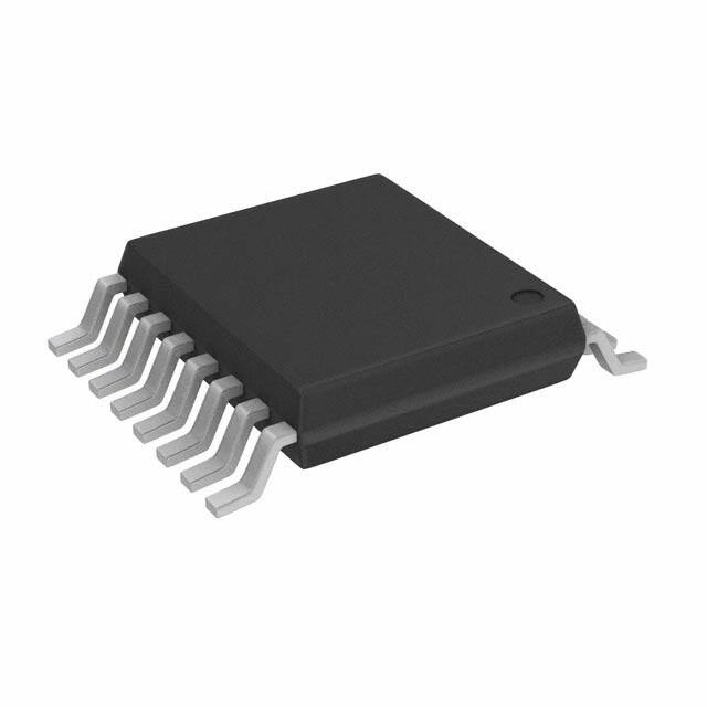
available in 16-pin TSSOP and SO packages. Refer to
the MAX9124 data sheet for a quad LVDS line driver.
�MAX9125/MAX9126
Quad LVDS Line Receivers with
Integrated Termination
ABSOLUTE MAXIMUM RATINGS
VCC to GND ...........................................................-0.3V to +4.0V
IN_+, IN_- to GND .................................................-0.3V to +4.0V
EN, EN to GND ...........................................-0.3V to (VCC + 0.3V)
OUT_ to GND .............................................-0.3V to (VCC + 0.3V)
Continuous Power Dissipation (TA = +70°C)
16-Pin TSSOP (derate 9.4mW/°C above +70°C) .........755mW
16-Pin SO (derate 8.7mW/°C above +70°C)................696mW
Storage Temperature Range .............................-65°C to +150°C
Maximum Junction Temperature .....................................+150°C
Operating Temperature Range ...........................-40°C to +85°C
Lead Temperature (soldering, 10s) .................................+300°C
ESD Protection (Human Body Model) IN_+, IN_-, OUT_............±7.5kV
Stresses beyond those listed under “Absolute Maximum Ratings” may cause permanent damage to the device. These are stress ratings only, and functional
operation of the device at these or any other conditions beyond those indicated in the operational sections of the specifications is not implied. Exposure to
absolute maximum rating conditions for extended periods may affect device reliability.
DC ELECTRICAL CHARACTERISTICS
(VCC = +3.0V to +3.6V, differential input voltage |VID| = 0.1V to 1.0V, common-mode voltage VCM = |VID/2| to 2.4V - |VID/2|, TA =
-40°C to +85°C. Typical values are at VCC = +3.3V, TA = +25°C, unless otherwise noted.) (Note 1)
PARAMETER
SYMBOL
CONDITIONS
MIN
TYP
MAX
UNITS
100
mV
LVDS INPUTS (IN_+, IN_-)
Differential Input High Threshold
VTH
Differential Input Low Threshold
VTL
-100
mV
0.1V ≤VID≤ 0.6V,
-20
20
Input Current (MAX9125)
IIN_+,
IIN_-
0.6V
很抱歉,暂时无法提供与“MAX9126EUE+”相匹配的价格&库存,您可以联系我们找货
免费人工找货