EVALUATION KIT AVAILABLE
MAX96706
14-Bit GMSL Deserializer
with Coax or STP Cable Input
General Description
The MAX96706 is a compact deserializer especially suited for automotive camera applications. Features include
adaptive equalization and an output crosspoint switch. An
embedded control channel operates at 9.6kbps to 1Mbps
in UART, I2C, and mixed UART/I2C modes, allowing programming of serializer, deserializer (SerDes), and camera
registers, independent of video timing.
The deserializer can track data from a spreadspectrum serial input. The serial input meets ISO 10605
and IEC 61000-4-2 ESD standards. The core supply
range is 1.7V to 1.9V and the I/O supply range is 1.7V
to 3.6V. The device is available in a 32-pin (5mm x 5mm)
TQFN and SWTQFN package with 0.5mm lead pitch and
operates over -40°C to +115°C temperature range.
Applications
●● Automotive Camera Applications
CAM
VIDEO
MAX96705
I 2C
MAX96706
GPU
I 2C
●● Ideal for Safety Camera Applications
• Works with Low-Cost 50Ω Coax (100Ω STP) Cable
• Error Detection of Video/Control Data
• High-Immunity Mode for Robust Control-Channel
EMC Tolerance
• Retransmission of Control Data Upon Error
• Best-in-Class Supply Current: 190mA (max)
• Adaptive Equalization for 15m Cable at Full Speed
• 32-Pin (5mm x 5mm) TQFN/SWTQFN Package
• Horizontal- and Vertical-Sync Encoding
and Tracking
●● High-Speed Deserialization for Megapixel Cameras
• Up to 1.74Gbps Serial-Bit Rate
• 6.25MHz to 87MHz x 12-Bit + H/V Data
• 36.66MHz to 116MHz x 12-Bit + H/V Data
(through Internal Encoding)
●● Multiple Modes for System Flexibility
• 9.6kbps to 1Mbps Control Channel in UART, I2C
(with Clock Stretch), or UART-to-I2C Modes
• 2:1 Input Mux for Camera Selection
• 15 Hardware-Selectable I2C-Device Addresses
• Pairs with Any Maxim GMSL Serializer
• Crosspoint Switch Maps Data to any Output
●● Reduces EMI and Shielding Requirements
Simplified Block Diagram
VIDEO
Benefits and Features
• Spread-Spectrum Serial-Input Tracking and Transfer
to the Parallel Output
• 1.7V to 1.9V Core and 1.7V to 3.6V I/O Supply
●● Peripheral Features for System Verification
• Built-In PRBS Receiver for BER Testing
• Eye-Width Monitor Allows In-System Test of HighSpeed Serial Link
• Dedicated “Up/Down” GPI for Camera Frame Sync
Trigger and Other Uses
●● Meets AEC-Q100 Automotive Specification
Ordering Information appears at end of data sheet.
19-8248; Rev 2; 11/18
• -40°C to +115°C Operating Temperature Range
• ±8kV Contact and ±15kV Air IEC 61000-4-2 and
ISO 10605 ESD Protection
�MAX96706
14-Bit GMSL Deserializer
with Coax or STP Cable Input
General Description . . . . . . . . . . . . . . . . . . . . . . . . . . . . . . . . . . . . . . . . . . . . . . . . . . . . . . . . . . . . . . . . . . . . . . . . . . . . 1
Applications . . . . . . . . . . . . . . . . . . . . . . . . . . . . . . . . . . . . . . . . . . . . . . . . . . . . . . . . . . . . . . . . . . . . . . . . . . . . . . . . . . . 1
Benefits and Features . . . . . . . . . . . . . . . . . . . . . . . . . . . . . . . . . . . . . . . . . . . . . . . . . . . . . . . . . . . . . . . . . . . . . . . . . . . 1
Simplified Block Diagram . . . . . . . . . . . . . . . . . . . . . . . . . . . . . . . . . . . . . . . . . . . . . . . . . . . . . . . . . . . . . . . . . . . . . . . . 1
Absolute Maximum Ratings . . . . . . . . . . . . . . . . . . . . . . . . . . . . . . . . . . . . . . . . . . . . . . . . . . . . . . . . . . . . . . . . . . . . . . 6
Package Thermal Characteristics . . . . . . . . . . . . . . . . . . . . . . . . . . . . . . . . . . . . . . . . . . . . . . . . . . . . . . . . . . . . . . . . . . 6
32-Pin TQFN-EP . . . . . . . . . . . . . . . . . . . . . . . . . . . . . . . . . . . . . . . . . . . . . . . . . . . . . . . . . . . . . . . . . . . . . . . . . . . . 6
DC Electrical Characteristics . . . . . . . . . . . . . . . . . . . . . . . . . . . . . . . . . . . . . . . . . . . . . . . . . . . . . . . . . . . . . . . . . . . . . 7
AC Electrical Characteristics . . . . . . . . . . . . . . . . . . . . . . . . . . . . . . . . . . . . . . . . . . . . . . . . . . . . . . . . . . . . . . . . . . . . 12
Typical Operating Characteristics . . . . . . . . . . . . . . . . . . . . . . . . . . . . . . . . . . . . . . . . . . . . . . . . . . . . . . . . . . . . . . . . . 15
Pin Configuration . . . . . . . . . . . . . . . . . . . . . . . . . . . . . . . . . . . . . . . . . . . . . . . . . . . . . . . . . . . . . . . . . . . . . . . . . . . . . . 16
Pin Description . . . . . . . . . . . . . . . . . . . . . . . . . . . . . . . . . . . . . . . . . . . . . . . . . . . . . . . . . . . . . . . . . . . . . . . . . . . . . . . 17
Functional Diagrams . . . . . . . . . . . . . . . . . . . . . . . . . . . . . . . . . . . . . . . . . . . . . . . . . . . . . . . . . . . . . . . . . . . . . . . . . . . 20
Detailed Description . . . . . . . . . . . . . . . . . . . . . . . . . . . . . . . . . . . . . . . . . . . . . . . . . . . . . . . . . . . . . . . . . . . . . . . . . . . 26
Serial Link Signaling and Data Format . . . . . . . . . . . . . . . . . . . . . . . . . . . . . . . . . . . . . . . . . . . . . . . . . . . . . . . . . . . . . 26
Operating Modes . . . . . . . . . . . . . . . . . . . . . . . . . . . . . . . . . . . . . . . . . . . . . . . . . . . . . . . . . . . . . . . . . . . . . . . . 26
Video/Configuration Link . . . . . . . . . . . . . . . . . . . . . . . . . . . . . . . . . . . . . . . . . . . . . . . . . . . . . . . . . . . . . . . . . . . 26
Single and Double Modes of Operation . . . . . . . . . . . . . . . . . . . . . . . . . . . . . . . . . . . . . . . . . . . . . . . . . . . . . . . 26
HS/VS Encoding . . . . . . . . . . . . . . . . . . . . . . . . . . . . . . . . . . . . . . . . . . . . . . . . . . . . . . . . . . . . . . . . . . . . . . . . . 26
Error Detection . . . . . . . . . . . . . . . . . . . . . . . . . . . . . . . . . . . . . . . . . . . . . . . . . . . . . . . . . . . . . . . . . . . . . . . . . . 26
Bus Widths . . . . . . . . . . . . . . . . . . . . . . . . . . . . . . . . . . . . . . . . . . . . . . . . . . . . . . . . . . . . . . . . . . . . . . . . . . . . . 27
Control Channel and Register Programming . . . . . . . . . . . . . . . . . . . . . . . . . . . . . . . . . . . . . . . . . . . . . . . . . . . . . . 30
Forward Control Channel . . . . . . . . . . . . . . . . . . . . . . . . . . . . . . . . . . . . . . . . . . . . . . . . . . . . . . . . . . . . . . . . . . 30
Reverse Control Channel . . . . . . . . . . . . . . . . . . . . . . . . . . . . . . . . . . . . . . . . . . . . . . . . . . . . . . . . . . . . . . . . . . 30
UART Interface . . . . . . . . . . . . . . . . . . . . . . . . . . . . . . . . . . . . . . . . . . . . . . . . . . . . . . . . . . . . . . . . . . . . . . . . . . 30
I2C Interface . . . . . . . . . . . . . . . . . . . . . . . . . . . . . . . . . . . . . . . . . . . . . . . . . . . . . . . . . . . . . . . . . . . . . . . . . . . . 30
Remote-End Operation . . . . . . . . . . . . . . . . . . . . . . . . . . . . . . . . . . . . . . . . . . . . . . . . . . . . . . . . . . . . . . . . . . . . 30
Clock-Stretch Timing . . . . . . . . . . . . . . . . . . . . . . . . . . . . . . . . . . . . . . . . . . . . . . . . . . . . . . . . . . . . . . . . . . . . . . 30
Packet-Based I2C . . . . . . . . . . . . . . . . . . . . . . . . . . . . . . . . . . . . . . . . . . . . . . . . . . . . . . . . . . . . . . . . . . . . . . . . 30
Packet Protocol Summary . . . . . . . . . . . . . . . . . . . . . . . . . . . . . . . . . . . . . . . . . . . . . . . . . . . . . . . . . . . . . . . . . 31
Control-Channel Error Detection and
Packet Retransmission . . . . . . . . . . . . . . . . . . . . . . . . . . . . . . . . . . . . . . . . . . . . . . . . . . . . . . . . . . . . . . . . . . . . 31
GPO/GPI Control . . . . . . . . . . . . . . . . . . . . . . . . . . . . . . . . . . . . . . . . . . . . . . . . . . . . . . . . . . . . . . . . . . . . . . . . . . . 31
Adaptive Line Equalizer . . . . . . . . . . . . . . . . . . . . . . . . . . . . . . . . . . . . . . . . . . . . . . . . . . . . . . . . . . . . . . . . . . . . . . 31
Eye-Width Monitor . . . . . . . . . . . . . . . . . . . . . . . . . . . . . . . . . . . . . . . . . . . . . . . . . . . . . . . . . . . . . . . . . . . . . . . . . . 31
Spread-Spectrum Tracking . . . . . . . . . . . . . . . . . . . . . . . . . . . . . . . . . . . . . . . . . . . . . . . . . . . . . . . . . . . . . . . . . . . 31
Cable-Type Configuration and Input MUX . . . . . . . . . . . . . . . . . . . . . . . . . . . . . . . . . . . . . . . . . . . . . . . . . . . . . . . . 31
Crosspoint Switch . . . . . . . . . . . . . . . . . . . . . . . . . . . . . . . . . . . . . . . . . . . . . . . . . . . . . . . . . . . . . . . . . . . . . . . . . . 32
www.maximintegrated.com
Maxim Integrated │ 2
�MAX96706
14-Bit GMSL Deserializer
with Coax or STP Cable Input
Shutdown/Sleep Modes . . . . . . . . . . . . . . . . . . . . . . . . . . . . . . . . . . . . . . . . . . . . . . . . . . . . . . . . . . . . . . . . . . . . . . 32
Configuration Link . . . . . . . . . . . . . . . . . . . . . . . . . . . . . . . . . . . . . . . . . . . . . . . . . . . . . . . . . . . . . . . . . . . . . . . . 32
Serialization Disable . . . . . . . . . . . . . . . . . . . . . . . . . . . . . . . . . . . . . . . . . . . . . . . . . . . . . . . . . . . . . . . . . . . . . . 32
Sleep Mode . . . . . . . . . . . . . . . . . . . . . . . . . . . . . . . . . . . . . . . . . . . . . . . . . . . . . . . . . . . . . . . . . . . . . . . . . . . . . 32
Power-Down Mode . . . . . . . . . . . . . . . . . . . . . . . . . . . . . . . . . . . . . . . . . . . . . . . . . . . . . . . . . . . . . . . . . . . . . . . 32
Link-Startup Procedure . . . . . . . . . . . . . . . . . . . . . . . . . . . . . . . . . . . . . . . . . . . . . . . . . . . . . . . . . . . . . . . . . . . . . . 32
Register Map . . . . . . . . . . . . . . . . . . . . . . . . . . . . . . . . . . . . . . . . . . . . . . . . . . . . . . . . . . . . . . . . . . . . . . . . . . . . . . . . . 34
Applications Information . . . . . . . . . . . . . . . . . . . . . . . . . . . . . . . . . . . . . . . . . . . . . . . . . . . . . . . . . . . . . . . . . . . . . . . . 62
Parallel Interface . . . . . . . . . . . . . . . . . . . . . . . . . . . . . . . . . . . . . . . . . . . . . . . . . . . . . . . . . . . . . . . . . . . . . . . . . . . 62
Bus Data Width . . . . . . . . . . . . . . . . . . . . . . . . . . . . . . . . . . . . . . . . . . . . . . . . . . . . . . . . . . . . . . . . . . . . . . . . . . 62
Bus Data Rates . . . . . . . . . . . . . . . . . . . . . . . . . . . . . . . . . . . . . . . . . . . . . . . . . . . . . . . . . . . . . . . . . . . . . . . . . . 62
Crossbar Switch . . . . . . . . . . . . . . . . . . . . . . . . . . . . . . . . . . . . . . . . . . . . . . . . . . . . . . . . . . . . . . . . . . . . . . . . . . . . 62
Crossbar Switch Programming . . . . . . . . . . . . . . . . . . . . . . . . . . . . . . . . . . . . . . . . . . . . . . . . . . . . . . . . . . . . . . 62
Recommended Crossbar Switch Programming Procedure . . . . . . . . . . . . . . . . . . . . . . . . . . . . . . . . . . . . . . . . 62
Control-Channel Interfaces . . . . . . . . . . . . . . . . . . . . . . . . . . . . . . . . . . . . . . . . . . . . . . . . . . . . . . . . . . . . . . . . . . . 65
I2C . . . . . . . . . . . . . . . . . . . . . . . . . . . . . . . . . . . . . . . . . . . . . . . . . . . . . . . . . . . . . . . . . . . . . . . . . . . . . . . . . . . . 65
I2C Bit Rate . . . . . . . . . . . . . . . . . . . . . . . . . . . . . . . . . . . . . . . . . . . . . . . . . . . . . . . . . . . . . . . . . . . . . . . . . . . . . 65
Software Programming of the Device Addresses . . . . . . . . . . . . . . . . . . . . . . . . . . . . . . . . . . . . . . . . . . . . . . . 65
I2C Address Translation . . . . . . . . . . . . . . . . . . . . . . . . . . . . . . . . . . . . . . . . . . . . . . . . . . . . . . . . . . . . . . . . . . . 65
Configuration Blocking . . . . . . . . . . . . . . . . . . . . . . . . . . . . . . . . . . . . . . . . . . . . . . . . . . . . . . . . . . . . . . . . . . . . 65
Cascaded/Parallel Devices . . . . . . . . . . . . . . . . . . . . . . . . . . . . . . . . . . . . . . . . . . . . . . . . . . . . . . . . . . . . . . . . . 65
Dual μC Control . . . . . . . . . . . . . . . . . . . . . . . . . . . . . . . . . . . . . . . . . . . . . . . . . . . . . . . . . . . . . . . . . . . . . . . . . 65
Packet-Based Control-Channel I2C . . . . . . . . . . . . . . . . . . . . . . . . . . . . . . . . . . . . . . . . . . . . . . . . . . . . . . . . . . 65
UART . . . . . . . . . . . . . . . . . . . . . . . . . . . . . . . . . . . . . . . . . . . . . . . . . . . . . . . . . . . . . . . . . . . . . . . . . . . . . . . . . . 66
Base Mode . . . . . . . . . . . . . . . . . . . . . . . . . . . . . . . . . . . . . . . . . . . . . . . . . . . . . . . . . . . . . . . . . . . . . . . . . . . . . 66
UART Timing . . . . . . . . . . . . . . . . . . . . . . . . . . . . . . . . . . . . . . . . . . . . . . . . . . . . . . . . . . . . . . . . . . . . . . . . . . . . 66
UART-to-I2C Conversion . . . . . . . . . . . . . . . . . . . . . . . . . . . . . . . . . . . . . . . . . . . . . . . . . . . . . . . . . . . . . . . . . . 67
UART Bypass Mode . . . . . . . . . . . . . . . . . . . . . . . . . . . . . . . . . . . . . . . . . . . . . . . . . . . . . . . . . . . . . . . . . . . . . . 68
Device Address . . . . . . . . . . . . . . . . . . . . . . . . . . . . . . . . . . . . . . . . . . . . . . . . . . . . . . . . . . . . . . . . . . . . . . . . . . 68
Cable Equalizer . . . . . . . . . . . . . . . . . . . . . . . . . . . . . . . . . . . . . . . . . . . . . . . . . . . . . . . . . . . . . . . . . . . . . . . . . . . . 68
ERRB Output . . . . . . . . . . . . . . . . . . . . . . . . . . . . . . . . . . . . . . . . . . . . . . . . . . . . . . . . . . . . . . . . . . . . . . . . . . . . . . 68
Auto-Error Reset . . . . . . . . . . . . . . . . . . . . . . . . . . . . . . . . . . . . . . . . . . . . . . . . . . . . . . . . . . . . . . . . . . . . . . . . . 68
Board Layout . . . . . . . . . . . . . . . . . . . . . . . . . . . . . . . . . . . . . . . . . . . . . . . . . . . . . . . . . . . . . . . . . . . . . . . . . . . . . . 68
Power-Supply Circuits and Bypassing . . . . . . . . . . . . . . . . . . . . . . . . . . . . . . . . . . . . . . . . . . . . . . . . . . . . . . . . 68
High-Frequency Signals . . . . . . . . . . . . . . . . . . . . . . . . . . . . . . . . . . . . . . . . . . . . . . . . . . . . . . . . . . . . . . . . . . . 68
ESD Protection . . . . . . . . . . . . . . . . . . . . . . . . . . . . . . . . . . . . . . . . . . . . . . . . . . . . . . . . . . . . . . . . . . . . . . . . . . . . . 69
Compatibility with Other GMSL Devices . . . . . . . . . . . . . . . . . . . . . . . . . . . . . . . . . . . . . . . . . . . . . . . . . . . . . . . . . 69
Device Configuration and Component Selection . . . . . . . . . . . . . . . . . . . . . . . . . . . . . . . . . . . . . . . . . . . . . . . . . . . 70
www.maximintegrated.com
Maxim Integrated │ 3
�MAX96706
14-Bit GMSL Deserializer
with Coax or STP Cable Input
Internal Input Pulldowns . . . . . . . . . . . . . . . . . . . . . . . . . . . . . . . . . . . . . . . . . . . . . . . . . . . . . . . . . . . . . . . . . . . 70
Multifunction Inputs . . . . . . . . . . . . . . . . . . . . . . . . . . . . . . . . . . . . . . . . . . . . . . . . . . . . . . . . . . . . . . . . . . . . . . . 70
I2C/UART Pullup Resistors . . . . . . . . . . . . . . . . . . . . . . . . . . . . . . . . . . . . . . . . . . . . . . . . . . . . . . . . . . . . . . . . . 70
AC-Coupling Capacitors . . . . . . . . . . . . . . . . . . . . . . . . . . . . . . . . . . . . . . . . . . . . . . . . . . . . . . . . . . . . . . . . . . . 70
Cables and Connectors . . . . . . . . . . . . . . . . . . . . . . . . . . . . . . . . . . . . . . . . . . . . . . . . . . . . . . . . . . . . . . . . . . . 70
PRBS . . . . . . . . . . . . . . . . . . . . . . . . . . . . . . . . . . . . . . . . . . . . . . . . . . . . . . . . . . . . . . . . . . . . . . . . . . . . . . . . . . . . 71
GPI/GPO . . . . . . . . . . . . . . . . . . . . . . . . . . . . . . . . . . . . . . . . . . . . . . . . . . . . . . . . . . . . . . . . . . . . . . . . . . . . . . . . . 71
Fast Detection of Loss-of-Lock . . . . . . . . . . . . . . . . . . . . . . . . . . . . . . . . . . . . . . . . . . . . . . . . . . . . . . . . . . . . . . 71
Providing a Frame Sync (Camera Applications) . . . . . . . . . . . . . . . . . . . . . . . . . . . . . . . . . . . . . . . . . . . . . . . . . 71
Entering/Exiting Sleep Mode . . . . . . . . . . . . . . . . . . . . . . . . . . . . . . . . . . . . . . . . . . . . . . . . . . . . . . . . . . . . . . . . . . 71
Legacy Control Channel . . . . . . . . . . . . . . . . . . . . . . . . . . . . . . . . . . . . . . . . . . . . . . . . . . . . . . . . . . . . . . . . . . . 71
Typical Application Circuit . . . . . . . . . . . . . . . . . . . . . . . . . . . . . . . . . . . . . . . . . . . . . . . . . . . . . . . . . . . . . . . . . . . . . . . 71
Ordering Information . . . . . . . . . . . . . . . . . . . . . . . . . . . . . . . . . . . . . . . . . . . . . . . . . . . . . . . . . . . . . . . . . . . . . . . . . . . 72
Revision History . . . . . . . . . . . . . . . . . . . . . . . . . . . . . . . . . . . . . . . . . . . . . . . . . . . . . . . . . . . . . . . . . . . . . . . . . . . . . . 73
Figure 1. Reverse Control-Channel Output Parameters . . . . . . . . . . . . . . . . . . . . . . . . . . . . . . . . . . . . . . . . . . . . . . . . 21
Figure 2. Test Circuit for Differential Input Measurement . . . . . . . . . . . . . . . . . . . . . . . . . . . . . . . . . . . . . . . . . . . . . . . 22
Figure 4. Line Fault . . . . . . . . . . . . . . . . . . . . . . . . . . . . . . . . . . . . . . . . . . . . . . . . . . . . . . . . . . . . . . . . . . . . . . . . . . . . 22
Figure 3. Test Circuit for Single-Ended Input Measurement . . . . . . . . . . . . . . . . . . . . . . . . . . . . . . . . . . . . . . . . . . . . 22
Figure 5. Worst-Case Pattern Output . . . . . . . . . . . . . . . . . . . . . . . . . . . . . . . . . . . . . . . . . . . . . . . . . . . . . . . . . . . . . . 23
Figure 6. I2C Timing Parameters . . . . . . . . . . . . . . . . . . . . . . . . . . . . . . . . . . . . . . . . . . . . . . . . . . . . . . . . . . . . . . . . . 23
Figure 7. Output Rise-and-Fall Times . . . . . . . . . . . . . . . . . . . . . . . . . . . . . . . . . . . . . . . . . . . . . . . . . . . . . . . . . . . . . . 23
Figure 8. Deserializer Delay . . . . . . . . . . . . . . . . . . . . . . . . . . . . . . . . . . . . . . . . . . . . . . . . . . . . . . . . . . . . . . . . . . . . . 24
Figure 9. GPI-to-GPO Delay . . . . . . . . . . . . . . . . . . . . . . . . . . . . . . . . . . . . . . . . . . . . . . . . . . . . . . . . . . . . . . . . . . . . . 24
Figure 10. Lock Time . . . . . . . . . . . . . . . . . . . . . . . . . . . . . . . . . . . . . . . . . . . . . . . . . . . . . . . . . . . . . . . . . . . . . . . . . . 24
Figure 11. Power-Up Delay . . . . . . . . . . . . . . . . . . . . . . . . . . . . . . . . . . . . . . . . . . . . . . . . . . . . . . . . . . . . . . . . . . . . . . 24
Figure 12. Active Output to High-Impedance Time, High Impedance to Active-Output Time Test Circuit . . . . . . . . . 25
Figure 13. Active Output to High-Impedance Time, High Impedance to Active-Output Time . . . . . . . . . . . . . . . . . . . 25
Figure 14. 24-Bit Mode Serial-Data Format . . . . . . . . . . . . . . . . . . . . . . . . . . . . . . . . . . . . . . . . . . . . . . . . . . . . . . . . . 27
Figure 15. 27-Bit High-Bandwidth Mode Serial-Data Format . . . . . . . . . . . . . . . . . . . . . . . . . . . . . . . . . . . . . . . . . . . . 28
Figure 16. 32-Bit Mode Serial-Data Format . . . . . . . . . . . . . . . . . . . . . . . . . . . . . . . . . . . . . . . . . . . . . . . . . . . . . . . . . 29
Figure 17. Coax Connection . . . . . . . . . . . . . . . . . . . . . . . . . . . . . . . . . . . . . . . . . . . . . . . . . . . . . . . . . . . . . . . . . . . . . 31
Figure 18. Crosspoint-Switch Dataflow . . . . . . . . . . . . . . . . . . . . . . . . . . . . . . . . . . . . . . . . . . . . . . . . . . . . . . . . . . . . . 31
Figure 19. State Diagram . . . . . . . . . . . . . . . . . . . . . . . . . . . . . . . . . . . . . . . . . . . . . . . . . . . . . . . . . . . . . . . . . . . . . . . 32
Figure 20. GMSL-UART Data Format for Base Mode . . . . . . . . . . . . . . . . . . . . . . . . . . . . . . . . . . . . . . . . . . . . . . . . . 66
www.maximintegrated.com
Maxim Integrated │ 4
�MAX96706
14-Bit GMSL Deserializer
with Coax or STP Cable Input
Figure 21. GMSL-UART Protocol for Base Mode . . . . . . . . . . . . . . . . . . . . . . . . . . . . . . . . . . . . . . . . . . . . . . . . . . . . . 66
Figure 22. Sync Byte (0x79) . . . . . . . . . . . . . . . . . . . . . . . . . . . . . . . . . . . . . . . . . . . . . . . . . . . . . . . . . . . . . . . . . . . . . 66
Figure 23. ACK Byte (0xC3) . . . . . . . . . . . . . . . . . . . . . . . . . . . . . . . . . . . . . . . . . . . . . . . . . . . . . . . . . . . . . . . . . . . . . 66
Figure 24. Format Conversion Between GMSL UART and I2C with Register Address (I2CMETHOD = 0) . . . . . . . . 67
Figure 25. Format Conversion Between GMSL UART and I2C with Register Address (I2CMETHOD = 1) . . . . . . . . 67
Figure 26. Human Body Model ESD Test Circuit . . . . . . . . . . . . . . . . . . . . . . . . . . . . . . . . . . . . . . . . . . . . . . . . . . . . . 69
Figure 27. IEC 61000-4-2 Contact Discharge ESD Test Circuit . . . . . . . . . . . . . . . . . . . . . . . . . . . . . . . . . . . . . . . . . . 69
Figure 28. ISO 10605 Contact Discharge ESD Test Circuit . . . . . . . . . . . . . . . . . . . . . . . . . . . . . . . . . . . . . . . . . . . . . 69
Table 1. Reverse Control-Channel Modes . . . . . . . . . . . . . . . . . . . . . . . . . . . . . . . . . . . . . . . . . . . . . . . . . . . . . . . . . . 30
Table 2. Link-Startup Procedure . . . . . . . . . . . . . . . . . . . . . . . . . . . . . . . . . . . . . . . . . . . . . . . . . . . . . . . . . . . . . . . . . . 33
Table 3. Output-Data Width Selection . . . . . . . . . . . . . . . . . . . . . . . . . . . . . . . . . . . . . . . . . . . . . . . . . . . . . . . . . . . . . 62
Table 4. Data-Rate Selection Table . . . . . . . . . . . . . . . . . . . . . . . . . . . . . . . . . . . . . . . . . . . . . . . . . . . . . . . . . . . . . . . 62
Table 5. Output Map (DBL = 0 or DBL = 1, First Word) . . . . . . . . . . . . . . . . . . . . . . . . . . . . . . . . . . . . . . . . . . . . . . . . 63
Table 6. Output Map (DBL = 1, Second Word) . . . . . . . . . . . . . . . . . . . . . . . . . . . . . . . . . . . . . . . . . . . . . . . . . . . . . . . 64
Table 7. Legend . . . . . . . . . . . . . . . . . . . . . . . . . . . . . . . . . . . . . . . . . . . . . . . . . . . . . . . . . . . . . . . . . . . . . . . . . . . . . . . 64
Table 8. Default-Device Address . . . . . . . . . . . . . . . . . . . . . . . . . . . . . . . . . . . . . . . . . . . . . . . . . . . . . . . . . . . . . . . . . 68
Table 9. Cable-Equalizer Boost Levels . . . . . . . . . . . . . . . . . . . . . . . . . . . . . . . . . . . . . . . . . . . . . . . . . . . . . . . . . . . . . 68
Table 10. Feature Compatibility . . . . . . . . . . . . . . . . . . . . . . . . . . . . . . . . . . . . . . . . . . . . . . . . . . . . . . . . . . . . . . . . . . 70
Table 11. Suggested Connectors and Cables for GMSL . . . . . . . . . . . . . . . . . . . . . . . . . . . . . . . . . . . . . . . . . . . . . . . 71
www.maximintegrated.com
Maxim Integrated │ 5
�MAX96706
14-Bit GMSL Deserializer
with Coax or STP Cable Input
Absolute Maximum Ratings
AVDD to EP*.........................................................-0.5V to +1.9V
DVDD to EP*.........................................................-0.5V to +1.9V
IOVDD to EP*........................................................-0.5V to +3.9V
LMN_ to EP* (15mA current limit).........................-0.5V to +3.9V
IN_+, IN_- to EP*..................................................-0.5V to +1.9V
All Other Pins to EP*.......................... -0.5V to (IOVDD + 0.5V)V
IN_+, IN_- Short Circuit to Ground or Supply............Continuous
Operating Temperature Range...........................-40°C to +115°C
Junction Temperature.......................................................+150°C
Storage Temperature Range............................. -40°C to +150°C
Soldering Temperature (reflow)........................................+260°C
Continuous Power Dissipation TA = +70°C, 32-pin TQFN/
SWTQFN (derate 34.5 mW/°C above +70°C.).......2758.6mW
*EP connected to IC ground.
Stresses beyond those listed under “Absolute Maximum Ratings” may cause permanent damage to the device. These are stress ratings only, and functional operation of the device at these
or any other conditions beyond those indicated in the operational sections of the specifications is not implied. Exposure to absolute maximum rating conditions for extended periods may affect
device reliability.
Package Thermal Characteristics
For the latest package outline information and land patterns (footprints), go to www.maximintegrated.com/packages. Note that a “+”,
“#”, or “-” in the package code indicates RoHS status only. Package drawings may show a different suffix character, but the drawing
pertains to the package regardless of RoHS status.
32-Pin TQFN-EP
PACKAGE CODE
T3255+8
Outline Number
21-0140
Land Pattern Number
90-0013
Thermal Resistance, Single Layer Board:
Junction-to-Ambient (θJA)
47
Junction-to-Case Thermal Resistance (θJC)
1.7
Thermal Resistance, Four Layer Board:
Junction-to-Ambient (θJA)
29
Junction-to-Case Thermal Resistance (θJC)
1.7
32-Pin SWTQFN-EP
PACKAGE CODE
T3255Y+8
Outline Number
21-100156
Land Pattern Number
90-100067
Thermal Resistance, Single Layer Board:
Junction-to-Ambient (θJA)
47
Junction-to-Case Thermal Resistance (θJC)
1.7
Thermal Resistance, Four Layer Board:
Junction-to-Ambient (θJA)
29
Junction-to-Case Thermal Resistance (θJC)
1.7
Package thermal resistances were obtained using the method described in JEDEC specification JESD51-7, using a four-layer board.
For detailed information on package thermal considerations, refer to www.maximintegrated.com/thermal-tutorial.
www.maximintegrated.com
Maxim Integrated │ 6
�MAX96706
14-Bit GMSL Deserializer
with Coax or STP Cable Input
DC Electrical Characteristics
(VDVDD = VAVDD = 1.7 to 1.9V, VIOVDD = 1.7V to 3.6V, RL = 100Ω ±1% (differential), EP connected to PCB ground, TA = -40°C to
+115°C, Typical values are at, VDVDD = VAVDD = VIOVDD = 1.8V, TA = +25°C, unless otherwise noted.) (Note 1)
PARAMETER
SYMBOL
CONDITIONS
MIN
TYP
MAX
UNITS
SINGLE-ENDED INPUTS (GPI, CXTP, I2CSEL, ADD_, HIM, PWDNB, MS)
High-Level Input Voltage
VIH1
Low-Level Input Voltage
VIL1
Input Current
IIN1
0.65 x
VIOVDD
VIN = 0 to VIOVDD
V
-20
0.35 x
VIOVDD
V
20
μA
SINGLE-ENDED OUTPUTS (DOUT_, VS, HS, DE, PCLKOUT)
High-Level
Output Voltage
VOH1
Low-Level
Output Voltage
VOL1
High-Impedance
Output Current
Output Short-Circuit Current
www.maximintegrated.com
IOZ
IOS
IOH = -2mA, DCS = 0
VIOVDD
- 0.3
IOH = -2mA, DCS = 1
VIOVDD
- 0.2
V
IOL = 2mA, DCS = 0
0.3
IOL = 2mA, DCS = 1
0.2
OUTENB = 1, VOUT = 0V or VIOVDD
-20
20
DOUT_, VO = 0V, DCS = 0,
VIOVDD = 3.0V to 3.6V
15
25
39
DOUT_, VO = 0V, DCS = 0,
VIOVDD = 1.7V to 1.9V
3
7
13
DOUT_, VO = 0V, DCS = 1,
VIOVDD = 3.0V to 3.6V
20
35
63
DOUT_, VO = 0V, DCS = 1,
VIOVDD = 1.7V to 1.9V
5
10
21
PCLKOUT_, VO = 0V, DCS = 0,
VIOVDD = 3.0V to 3.6V
15
33
50
PCLKOUT_, VO = 0V, DCS = 0,
VIOVDD = 1.7V to 1.9V
5
10
17
PCLKOUT_, VO = 0V, DCS = 1,
VIOVDD = 3.0V to 3.6V
30
54
97
PCLKOUT_, VO = 0V, DCS = 1,
VIOVDD = 1.7V to 1.9V
9
16
32
V
μA
mA
Maxim Integrated │ 7
�MAX96706
14-Bit GMSL Deserializer
with Coax or STP Cable Input
DC Electrical Characteristics (continued)
(VDVDD = VAVDD = 1.7 to 1.9V, VIOVDD = 1.7V to 3.6V, RL = 100Ω ±1% (differential), EP connected to PCB ground, TA = -40°C to
+115°C, Typical values are at, VDVDD = VAVDD = VIOVDD = 1.8V, TA = +25°C, unless otherwise noted.) (Note 1)
PARAMETER
SYMBOL
CONDITIONS
MIN
TYP
MAX
UNITS
UART/I2C and GENERAL-PURPOSE I/Os (RX/SDA, TX/SCL, GPIO_, ERRB, LOCK, LFLTB) with OPEN-DRAIN OUTPUTS
High-Level Input Voltage
VIH2
Low-Level Input Voltage
VIL2
Input Current
0.7 x
VIOVDD
V
0.3 x
VIOVDD
IIN2
VIN = 0 to VIOVDD (Note 2), RX/SDA,
TX/SCL
-110
5
IIN
VIN = 0 to VIOVDD (Note 2), GPIO_,
ERRB, LOCK
-80
5
Low-Level Open-Drain Output
Voltage
VOL
Input Capacitance
CIN
V
μA
IOL = 3mA, VIOVDD = 1.7V to 1.9V
0.4
IOL = 3mA, VIOVDD = 3.0V to 3.6V
0.3
Each pin (Note 3)
10
V
pF
OUTPUTS FOR REVERSE CONTROL CHANNEL (IN0+, IN0-, IN1+, IN1-)
Differential High-Output Peak
Voltage (VIN+ - VIN-)
Differential Low-Output Peak
Voltage (VIN+ - VIN-)
Single-Ended High-Output
Peak Voltage
www.maximintegrated.com
VRODH
VRODL
VROSH
Forward channel disabled,
normal-immunity mode (Figure 1)
30
60
Forward channel disabled, high-immunity
mode (Figure 1)
50
100
Forward channel disabled,
normal-immunity mode (Figure 1)
-60
-30
Forward channel disabled, high-immunity
mode (Figure 1)
-100
-50
Forward channel disabled,
normal-immunity mode (Figure 1)
30
60
Forward channel disabled, high-immunity
mode (Figure 1)
50
100
mV
mV
mV
Maxim Integrated │ 8
�MAX96706
14-Bit GMSL Deserializer
with Coax or STP Cable Input
DC Electrical Characteristics (continued)
(VDVDD = VAVDD = 1.7 to 1.9V, VIOVDD = 1.7V to 3.6V, RL = 100Ω ±1% (differential), EP connected to PCB ground, TA = -40°C to
+115°C, Typical values are at, VDVDD = VAVDD = VIOVDD = 1.8V, TA = +25°C, unless otherwise noted.) (Note 1)
PARAMETER
Single-Ended Low-Output
Peak Voltage
SYMBOL
VROSL
CONDITIONS
MIN
TYP
MAX
Forward channel disabled,
normal-immunity mode (Figure 1)
-60
-30
Forward channel disabled, high-immunity
mode (Figure 1)
-100
-50
UNITS
mV
DIFFERENTIAL INPUTS (IN0+, IN0-, IN1+, IN1-)
Differential High-Input
Threshold Peak Voltage
(VIN+ - VIN-)
VIDH(P)
Activity detector, medium threshold
(0x22 D[6:5] = 01) (Figure 2)
60
Activity detector, low threshold
(0x22 D[6:5] = 00) (Figure 2)
49
mV
Activity detector, medium threshold
(0x22 D[6:5] = 01) (Figure 2)
-60
Activity detector, low threshold
(0x22 D[6:5] = 00) (Figure 2)
-49
Differential Low-Input
Threshold Peak Voltage
(VIN+ - VIN-)
VIDL(P)
Input Common-Mode Voltage
(VIN+ + VIN-)/2
VCMR
1
1.3
1.6
V
Differential-Input Resistance
(Internal)
RI
80
100
130
Ω
mV
SINGLE-ENDED INPUTS (IN0+, IN0-, IN1+, IN1-)
Single-Ended High-Input
Threshold Peak Voltage
Single-Ended Low-Input
Threshold Peak Voltage
Input Resistance (Internal)
VISH(P)
VISL(P)
Activity detector, medium threshold
(0x22 D[6:5] = 01) (Figure 3)
43
Activity detector, low threshold
(0x22 D[6:5] = 00) (Figure 3)
33
mV
Activity detector, medium threshold
(0x22 D[6:5] = 01) (Figure 3)
-43
Activity detector, low threshold
(0x22 D[6:5] = 00) (Figure 3)
-33
RI
mV
40
50
65
Ω
0.3
V
0.57
1.07
V
V
V
LINE FAULT DETECTION INPUTS (LMN0, LMN1)
Short-to-Ground Threshold
VTG
(Figure 4)
Normal Threshold
VTN
(Figure 4)
Open Threshold
VTO
(Figure 4)
1.45
VIO +
0.06
Open-Input Voltage
VIO
(Figure 4)
1.47
1.75
Short-to-Battery Threshold
VTE
(Figure 4)
2.47
www.maximintegrated.com
V
Maxim Integrated │ 9
�MAX96706
14-Bit GMSL Deserializer
with Coax or STP Cable Input
DC Electrical Characteristics (continued)
(VDVDD = VAVDD = 1.7 to 1.9V, VIOVDD = 1.7V to 3.6V, RL = 100Ω ±1% (differential), EP connected to PCB ground, TA = -40°C to
+115°C, Typical values are at, VDVDD = VAVDD = VIOVDD = 1.8V, TA = +25°C, unless otherwise noted.) (Note 1)
PARAMETER
SYMBOL
CONDITIONS
MIN
TYP
MAX
fPCLKOUT = 116MHz, HIBW = 1, BWS = 0,
double output, AVDD + DVDD (1.9V)
100
120
fPCLKOUT = 116MHz, HIBW = 0, BWS = 0,
double output, AVDD + DVDD (1.9V)
95
115
fPCLKOUT = 116MHz, BWS = 0, double
output, IOVDD (1.9V) CL = 5pF
(DCS = 0) (Note 3)
22
25
fPCLKOUT = 116MHz, BWS = 0, double
output, IOVDD (1.9V), CL = 10pF
(DCS = 1) (Note 3)
31
35
fPCLKOUT = 116MHz, BWS = 0, double
output, IOVDD (3.6V), CL = 5pF
(DCS = 0) (Note 3)
44
49
fPCLKOUT = 116MHz, BWS = 0, double
output, IOVDD (3.6V), CL = 10pF
(DCS = 1) (Note 3)
63
70
fPCLKOUT = 87MHz, BWS = 1, double
output, IOVDD (1.9V), AVDD + DVDD
(1.9V)
95
115
fPCLKOUT = 87MHz, BWS = 1, double
output, IOVDD (1.9V), CL = 5pF (DCS = 0)
(Note 3)
17
19
fPCLKOUT = 87MHz, BWS = 1, double
output, IOVDD (1.9V), CL = 10pF
(DCS = 1) (Note 3)
24
27
fPCLKOUT = 87MHz, BWS = 1, double
output, IOVDD (3.6V), CL = 5pF (DCS = 0)
(Note 3)
33
36
fPCLKOUT = 87MHz, BWS = 1, double
output, IOVDD (3.6V), CL = 10pF
(DCS = 1) (Note 3)
44
49
fPCLKOUT = 58MHz, HIBW = 1, BWS = 0,
single output, AVDD + DVDD (1.9V)
70
84
fPCLKOUT = 58MHz, HIBW = 0, BWS = 0,
single output, AVDD + DVDD (1.9V)
70
84
fPCLKOUT = 58MHz, BWS = 0, single
output, IOVDD (1.9V), CL = 5pF
(DCS = 0) (Note 3)
11
13
fPCLKOUT = 58MHz, BWS = 0, single
output, IOVDD (3.6V), CL = 10pF
(DCS = 1) (Note 3)
15
18
UNITS
POWER SUPPLY
Worst-Case Supply Current
(Figure 5)
www.maximintegrated.com
IWCS
mA
Maxim Integrated │ 10
�MAX96706
14-Bit GMSL Deserializer
with Coax or STP Cable Input
DC Electrical Characteristics (continued)
(VDVDD = VAVDD = 1.7 to 1.9V, VIOVDD = 1.7V to 3.6V, RL = 100Ω ±1% (differential), EP connected to PCB ground, TA = -40°C to
+115°C, Typical values are at, VDVDD = VAVDD = VIOVDD = 1.8V, TA = +25°C, unless otherwise noted.) (Note 1)
PARAMETER
SYMBOL
CONDITIONS
MIN
TYP
MAX
UNITS
fPCLKOUT = 58MHz, BWS = 0, single
output, IOVDD (3.6V), CL = 5pF
(DCS = 0) (Note 3)
22
25
fPCLKOUT = 58MHz, BWS = 0, single
output, IOVDD (3.6V), CL = 10pF
(DCS = 1) (Note 3)
30
34
fPCLKOUT = 43.5MHz, BWS = 1, single
output, AVDD + DVDD (1.9V)
70
84
fPCLKOUT = 43.5MHz, BWS = 1, single
output, IOVDD (1.9V), CL = 5pF
(DCS = 0) (Note 3)
8
10
fPCLKOUT = 43.5MHz, BWS = 1, single
output, IOVDD (1.9V), CL = 10pF
(DCS = 1) (Note 3)
12
14
fPCLKOUT = 43.5MHz, BWS = 1, single
output, IOVDD (3.6V), CL = 5pF
(DCS = 0) (Note 3)
16
18
fPCLKOUT = 43.5MHz, BWS = 1, single
output, IOVDD (3.6V), CL = 10pF
(DCS = 1) (Note 3)
22
25
Wake-up receivers enabled
54
160
Wake-up receivers disabled
15
100
PWDNB = low
15
100
Human Body Model, RD = 1.5kΩ,
CS = 100pF
±8
IEC 61000-4-2, RD = 330Ω, CS = 150pF,
Contact discharge
±10
IEC 61000-4-2, RD = 330Ω, CS = 150pF,
Air discharge
±15
ISO 10605, RD = 2kΩ, CS = 330pF,
Contact discharge
±10
ISO 10605, RD = 2kΩ, CS = 330pF,
Air discharge
±30
Human Body Model, RD = 1.5kΩ,
CS = 100pF
±4
kV
Machine Model
250
V
POWER SUPPLY (continued)
Worst-Case Supply Current
(Figure 5) (continued)
IWCS
Sleep-Mode Supply Current
ICCS
Power-Down Supply Current
ICCZ
mA
μA
μA
ESD PROTECTION
IN+, IN- (Note 4)
All Other Pins (Note 5)
www.maximintegrated.com
VESD
VESD
kV
Maxim Integrated │ 11
�MAX96706
14-Bit GMSL Deserializer
with Coax or STP Cable Input
AC Electrical Characteristics
(VDVDD = VAVDD = 1.7 to 1.9V, VIOVDD = 1.7V to 3.6V, RL = 100Ω ±1% (differential), EP connected to PCB ground, TA = -40°C to
+115°C, Typical values are at, VDVDD = VAVDD = VIOVDD = 1.8V, TA = +25°C, unless otherwise noted.) (Note 1)
PARAMETER
SYMBOL
CONDITIONS
MIN
TYP
MAX
UNITS
PARALLEL CLOCK OUTPUT (PCLKOUT)
Clock Frequency
BWS = 1, DRS = 1, single output
6.25
12.5
BWS = 0, DRS = 1, single output
8.33
16.66
BWS = 1, DRS = 0, single output
12.5
43.5
BWS = 0, HIBW = 0, DRS = 0,
single output
16.66
58
fPCLKOUT BWS = 0, HIBW = 1, DRS = 0,
single output
36.66
58
25
87
BWS = 0, HIBW = 0, DRS = 0,
double output
33.33
116
BWS = 0, HIBW = 1, DRS = 0,
double output
73.33
116
PCLKOUT and DOUT_, DCS = 1,
CL = 10pF or DCS = 0, CL = 5pF,
nonstaggered DOUT_
0.4T
PCLKOUT and DOUT_, DCS = 1,
CL = 10pF or DCS = 0, CL = 5pF,
staggered DOUT_
0.35T
0.4T
PCLKOUT and DOUT_, DCS = 1,
CL = 10pF or DCS = 0, CL = 5pF,
nonstaggered DOUT_
0.35T
0.4T
PCLKOUT and DOUT_, DCS = 1, CL =
10pF or DCS = 0, CL = 5pF,
staggered DOUT_
0.3T
BWS = 1, DRS = 0, double output
Data Valid Before Clock
Data Valid After Clock
Clock Jitter
tDVB
tDVA
tJ
MHz
0.5T
ns
ns
0.35T
RMS period jitter, spread off, 1.74Gbps
PRBS pattern, UI = 1/fPCLKOUT, DBL = 1,
double output)
0.05
Period jitter; peak-to-peak, spread off,
1.74Gbps, PRBS pattern, UI = 1/fPCLKOUT,
DBL = 0, single output)
0.01
UI
I2C/UART PORT TIMING
I2C/UART Bit Rate
Output Rise Time
tR
30% to 70%, CL = 10pF to 100pF,
1kΩ pullup to IOVDD
Output Fall Time
tF
70% to 30%, CL = 10pF to 100pF,
1kΩ pullup to IOVDD
www.maximintegrated.com
9.6
1000
kbps
20
150
ns
20
150
ns
Maxim Integrated │ 12
�MAX96706
14-Bit GMSL Deserializer
with Coax or STP Cable Input
AC Electrical Characteristics (continued)
(VDVDD = VAVDD = 1.7 to 1.9V, VIOVDD = 1.7V to 3.6V, RL = 100Ω ±1% (differential), EP connected to PCB ground, TA = -40°C to
+115°C, Typical values are at, VDVDD = VAVDD = VIOVDD = 1.8V, TA = +25°C, unless otherwise noted.) (Note 1)
PARAMETER
SYMBOL
CONDITIONS
MIN
TYP
MAX
UNITS
I2C TIMING (Figure 6)
Low fSCL range: (I2CMSTBT = 010,
I2CSLVSH = 10)
SCL Clock Frequency
fSCL
9.6
100
Mid fSCL range: (I2CMSTBT 101,
I2CSLVSH = 01)
>100
400
High fSCL range: (I2CMSTBT = 111,
I2CSLVSH = 00)
>400
1000
fSCL range, Low
START Condition Hold Time
Low Period of SCL Clock
High Period of SCL Clock
tHD:STA
tLOW
tHIGH
Repeated START Condition
Setup Time
tSU:STA
Data Hold Time
tHD:DAT
Data Setup Time
Setup Time for STOP
Condition
Bus Free Time
Data Valid Time
Data Valid Acknowledge Time
www.maximintegrated.com
tSU:DAT
tSU:STO
tBUF
tVD:DAT
tVD:ACK
kHz
4
fSCL range, Mid
0.6
fSCL range, High
0.26
fSCL range, Low
4.7
fSCL range, Mid
1.3
fSCL range, High
0.5
fSCL range, Low
4
fSCL range, Mid
0.6
fSCL range, High
0.26
fSCL range, Low
4.7
fSCL range, Mid
0.6
fSCL range, High
0.26
fSCL range, Low
0
fSCL range, Mid
0
fSCL range, High
0
fSCL range, Low
250
fSCL range, Mid
100
fSCL range, High
50
fSCL range, Low
4
fSCL range, Mid
0.6
fSCL range, High
0.26
fSCL range, Low
4.7
fSCL range, Mid
1.3
fSCL range, High
0.5
µs
µs
µs
µs
ns
ns
µs
µs
fSCL range, Low
3.45
fSCL range, Mid
0.9
fSCL range, High
0.45
fSCL range, Low
3.45
fSCL range, Mid
0.9
fSCL range, High
0.45
µs
µs
Maxim Integrated │ 13
�MAX96706
14-Bit GMSL Deserializer
with Coax or STP Cable Input
AC Electrical Characteristics (continued)
(VDVDD = VAVDD = 1.7 to 1.9V, VIOVDD = 1.7V to 3.6V, RL = 100Ω ±1% (differential), EP connected to PCB ground, TA = -40°C to
+115°C, Typical values are at, VDVDD = VAVDD = VIOVDD = 1.8V, TA = +25°C, unless otherwise noted.) (Note 1)
PARAMETER
SYMBOL
Pulse Width of Spikes
Suppressed
tSP
Capacitive load each bus line
CB
CONDITIONS
MIN
TYP
MAX
fSCL range, Low
50
fSCL range, Mid
50
fSCL range, High
UNITS
ns
50
100
pF
SWITCHING CHARACTERISTICS (Note 3)
PCLKOUT Rise-and-Fall Time
(Figure 7)
Parallel Data Rise-and-Fall
Time (Figure 7)
tR, tF
tR, tF
20% to 80%, VIOVDD = 1.7V to 1.9V,
DCS = 1, CL = 10pF
0.4
2.2
20% to 80%, VIOVDD = 1.7V to 1.9V,
DCS = 0, CL = 5pF
0.5
2.8
20% to 80%, VIOVDD = 3.0V to 3.6V,
DCS = 1, CL = 10pF
0.25
1.8
20% to 80%, VIOVDD = 3.0V to 3.6V,
DCS = 0, CL = 5pF
0.3
2
20% to 80%, VIOVDD = 1.7V to 1.9V,
DCS = 1, CL = 10pF
0.5
3.1
20% to 80%, VIOVDD = 1.7V to 1.9V,
DCS = 0, CL = 5pF
0.6
3.8
20% to 80%, VIOVDD = 3.0V to 3.6V,
DCS = 1, CL = 10pF
0.3
2.2
20% to 80%, VIOVDD = 3.0V to 3.6V,
DCS = 0, CL = 5pF
0.4
2.4
Deserializer Delay
tSD
(Figure 8) (Note 6)
Reverse Control-Channel
Output Rise Time
tR
No forward-channel data transmission
Reverse Control-Channel
Output Fall Time
tF
No forward-channel data transmission
GPI-to-GPO Delay
Lock Time (Note 3)
Power-Up Time
tGPIO
tLOCK
ns
ns
2160
Bits
180
400
ns
180
400
ns
Deserializer GPI to serializer GPO
(Figure 9)
350
µs
(Figure 10) AEQ on, packet CC off
1.6
(Figure 10) AEQ on, packet CC on
4.1
(Figure 10) AEQ off, packet CC off
1
(Figure 10) AEQ off, packet CC on
3.5
ms
tPU
(Figure 11)
6.5
ms
Active Output to High-Impedance Time
tOAZ
(Figure 12, Figure 13)
CC write OUTENB =1
250
ns
Active High-Impedance to
Output Time
tOZA
(Figure 12, Figure 13)
CC write OUTENB =0
250
ns
Note
Note
Note
Note
Note
Note
1: Limits are 100% production tested at TA = +115°C. Limits over the operating temperature range are guaranteed by design
and characterization, unless otherwise noted.
2: IIN min is due to voltage drop across the internal pullup resistor.
3: Not production tested. Guaranteed by design.
4: Specified pin to ground.
5: Specified pin to all supply/ground.
6: Measured in serial link bit times. Bit time = 1/(30 x fPCLKOUT) for BWS = GND. Bit time = 1/(40 x fPCLKOUT) for BWS = 1.
www.maximintegrated.com
Maxim Integrated │ 14
�MAX96706
14-Bit GMSL Deserializer
with Coax or STP Cable Input
Typical Operating Characteristics
(VAVDD = VDVDD = VIOVDD = 1.8V, TA = +25°C, unless otherwise noted.)
SUPPLY CURRENT vs.
PIXEL CLOCK FREQUENCY (BWS = 0, HIBW = 1)
SUPPLY CURRENT vs.
PIXEL CLOCK FREQUENCY (BWS = 0, HIBW = 0)
SUPPLY CURRENT (mA)
90
toc01
PRBS ON,
COAX MODE
DBL = 0
70
60
DBL = 1
50
35
55
75
95
70
60
40
115
DBL = 0
15
35
80
DBL = 0
70
60
50
40
EQ OFF
10
30
50
70
95
115
toc04
70
DBL = 1
PIXEL CLOCK FREQUENCY (MHz)
SUPPLY CURRENT (mA)
90
75
MAXIMUM PIXEL CLOCK FREQUENCY vs.
STP CABLE LENGTH (BER < 10-10)
toc03
EQ ON
55
PIXEL CLOCK FREQUENCY (MHz)
SUPPLY CURRENT vs.
PIXEL CLOCK FREQUENCY (BWS = 1, HIBW = 0)
PRBS ON,
COAX MODE
DBL = 1
EQ OFF
PIXEL CLOCK FREQUENCY (MHz)
100
EQ OFF
80
50
EQ OFF
15
PRBS ON,
COAX MODE
90
80
40
toc02
100
EQ ON
SUPPLY CURRENT (mA)
100
AEQ
60
50
40
9.7dB EQ
NO EQ
30
4.3dB EQ
20
10
0
90
NO PE, DBL = 0
BER CAN BE AS LOW AS 10-12 FOR
CABLE LENGTHS LESS THAN 15m
0
5
PIXEL CLOCK FREQUENCY (MHz)
10
15
20
25
STP CABLE LENGTH (m)
MAXIMUM PIXEL CLOCK FREQUENCY vs.
COAX CABLE LENGTH (BER < 10-10)
toc05
PIXEL CLOCK FREQUENCY (MHz)
70
NO PE, DBL = 0
AEQ
60
50
40
NO EQ
30
4.3dB EQ
20
10
0
BER CAN BE AS LOW AS 10-12 FOR
CABLE LENGTHS LESS THAN 15m
0
10
20
30
40
COAX CABLE LENGTH (m)
www.maximintegrated.com
Maxim Integrated │ 15
�MAX96706
14-Bit GMSL Deserializer
with Coax or STP Cable Input
DOUT6/ADD0
IOVDD
PCLKOUT
DOUT7/ADD1
DOUT8/ADD2
DOUT9/ADD3
DOUT10/I2CSEL
TOP VIEW
DOUT5/HIM
Pin Configuration
24
23
22
21
20
19
18
17
DOUT4
25
16
DOUT11/CXTP/DE
DOUT3
26
15
DOUT12/HS
PWDNB
27
14
DOUT13/VS
LFLTB
28
13
DVDD
DOUT2
29
12
LOCK
DOUT1
30
11
ERRB
DOUT0
31
10
TX/SCL
MS
32
9
RX/SDA
MAX96706
1
2
3
4
5
6
7
8
GPI
LMN1
IN1+
IN1-
AVDD
IN0+
IN0-
LMN0
+
TQFN/
SWTQFN
(5mm x 5mm)
www.maximintegrated.com
Maxim Integrated │ 16
�MAX96706
14-Bit GMSL Deserializer
with Coax or STP Cable Input
Pin Description
PIN
NAME
FUNCTION
REF SUPPLY
TYPE
POWER
5
AVDD
1.8V Analog Power Supply. Bypass AVDD to EP with 0.1μF and
0.001μF capacitors placed as close as possible to the device, with
the smaller-value capacitor closest to AVDD.
Power
13
DVDD
1.8V Digital Power Supply. Bypass DVDD to EP with 0.1μF and
0.001μF capacitors placed as close as possible to the device, with
the smaller-value capacitor closest to DVDD.
Power
22
IOVDD
I/O Supply Voltage. 1.8V to 3.3V logic I/O power supply. Bypass
IOVDD to EP with 0.1μF and 0.001μF capacitors placed as close
as possible to the device, with the smaller-value capacitor closest
to IOVDD.
Power
EP
—
Exposed Pad. EP is internally connected to device ground. Must
connect EP to the PCB ground plane through a via array for proper
thermal and electrical performance.
Power
HIGH-SPEED DIGITAL
High-Speed Digital / Multifunction
14
DOUT13/VS
Parallel-Data/Vertical-Sync Output. Defaults to parallel-data
output on power-up. Vertical-sync output when HS/VS encoding is
enabled, or when in high-bandwidth mode.
IOVDD
Digital
15
DOUT12/HS
Parallel-Data/Horizontal-Sync Output. Defaults to parallel-data
output on power-up. Horizontal-sync output when HS/VS encoding
is enabled, or when in high-bandwidth mode.
IOVDD
Digital
DOUT11/
CXTP/DE
Parallel-Data Output/Cable-Type Input/Data-Enable Output with
internal pulldown to EP. CX/TP is latched at power-up, or when
resuming from power-down mode (PWDNB = low), and switches
to parallel/data-enable output after power-up. Connect CXTP to
IOVDD with a 30kΩ resistor to set high (coax mode), or leave open
to set low (twisted-pair mode). Data-enable output when HIBW = 1.
IOVDD
Digital
DOUT10/
I2CSEL
Parallel-Data Output/I2C-Select Input with Internal Pulldown to EP.
I2CSEL is latched at power-up, or when resuming from powerdown mode (PWDNB = low), and switches to parallel-data output
after power-up. Connect I2CSEL to IOVDD with a 30kΩ resistor to
set high (I2C interface), or leave open to set low (UART interface).
IOVDD
Digital
DOUT9/
ADD3
Parallel-Data Output/Address Input with Internal Pulldown to EP.
ADD3 is latched at power-up, or when resuming from power-down
mode (PWDNB = low), and switches to parallel-data output after
power-up. Connect ADD3 to IOVDD with a 30kΩ resistor to set
high, or leave open to set low.
IOVDD
Digital
DOUT8/
ADD2
Parallel-Data Output/Address Input with Internal Pulldown to EP.
ADD2 is latched at power-up, or when resuming from power-down
mode (PWDNB = low), and switches to parallel-data output after
power-up. Connect ADD2 to IOVDD with a 30kΩ resistor to set
high, or leave open to set low.
IOVDD
Digital
16
17
18
19
www.maximintegrated.com
Maxim Integrated │ 17
�MAX96706
14-Bit GMSL Deserializer
with Coax or STP Cable Input
Pin Description (continued)
PIN
20
23
24
REF SUPPLY
TYPE
DOUT7/
ADD1
Parallel-Data Output/Address Input with Internal Pulldown to EP.
ADD1 is latched at power-up, or when resuming from power-down
mode (PWDNB = low), and switches to parallel-data output after
power-up. Connect ADD1 to IOVDD with a 30kΩ resistor to set
high, or leave open to set low.
IOVDD
Digital
DOUT6/
ADD0
Parallel-Data Output/Address Input with Internal Pulldown to EP.
ADD0 is latched at power-up, or when resuming from power-down
mode (PWDNB = low), and switches to parallel-data output after
power-up. Connect ADD0 to IOVDD with a 30kΩ resistor to set
high, or leave open to set low.
IOVDD
Digital
DOUT5/HIM
Parallel-Data Output/High-Immunity Mode Input with Internal
Pulldown to EP. HIM input latched at power-up, or when resuming
from power-down mode (PWDNB = low), and switches to paralleldata output after power-up. Connect HIM to IOVDD with a 30kΩ
resistor to set high, or leave open to set low. HIGHIMM in the
serializer must be set to the same value.
IOVDD
Digital
Parallel-Clock Output. Provides timing signal to latch parallel-data
outputs to the input of another device.
IOVDD
Digital
NAME
FUNCTION
High-Speed Digital / Single-Function
21
PCLKOUT
25
DOUT4
Parallel-Data Output
IOVDD
Digital
26
DOUT3
Parallel-Data Output
IOVDD
Digital
29
DOUT2
Parallel-Data Output
IOVDD
Digital
30
DOUT1
Parallel-Data Output
IOVDD
Digital
31
DOUT0
Parallel-Data Output
IOVDD
Digital
LINE FAULT
2
LMN1
Line-Fault Monitor Input 1 (see Figure 4)
Analog
8
LMN0
Line-Fault Monitor Input 0 ) (see Figure 4)
Analog
LFLTB
Line-Fault Output. LFLTB is active low, and has a 60kΩ internal pullup
to IOVDD. LFLTB low indicates a line-fault condition at LMN0, or
LMN1. LFLTB is output high when PWDNB is low.
28
www.maximintegrated.com
IOVDD
Digital
Maxim Integrated │ 18
�MAX96706
14-Bit GMSL Deserializer
with Coax or STP Cable Input
Pin Description (continued)
REF SUPPLY
TYPE
IOVDD
Digital
RX/SDA
Receive/Serial Data. Input/output with internal 30kΩ pullup to
IOVDD. In UART mode, RX/SDA is the Rx input of the serializer's
UART. In I2C mode, RX/SDA is the SDA input/output of the serializer's I2C master/slave. RX/SDA has an open-drain driver and
requires a pullup resistor.
IOVDD
Digital
TX/SCL
Transmit/Serial Clock. Input/output with internal 30kΩ pullup to
IOVDD. In UART mode, TX/SCL is the Tx output of the serializer's
UART. In I2C mode, TX/SCL is the SCL input/output of the serializer's I2C master/slave. TX/SCL has an open-drain driver and
requires a pullup resistor.
IOVDD
Digital
ERRB
Error Output. Active-low, open-drain video data error output with
internal pullup to IOVDD. ERRB goes low when decoding errors
during normal operation exceed a programmed threshold, or when
at least one PRBS error is detected during a PRBS test. ERRB is
output high when PWDNB is low.
IOVDD
Digital
12
LOCK
Lock Output. Open-drain output with internal pullup to IOVDD.
LOCK high indicates PLLs are locked with correct serial-word
boundary alignment. LOCK low indicates PLLs are not locked, or
incorrect serial-word boundary alignment. LOCK is low when the
configuration link is active. LOCK is output high when PWDNB is
low.
IOVDD
Digital
27
PWDNB
Active-Low, Power-Down Input with Internal Pulldown to EP.
Set PWDNB low to enter power-down mode to reduce power
consumption.
IOVDD
Digital
32
MS
Mode-select Input with Internal Pulldown to EP. Set MS low to
select base mode. Set MS high to select bypass mode.
IOVDD
Digital
PIN
NAME
FUNCTION
OTHER PINS
1
GPI
General-Purpose Input with Internal Pulldown to EP. Serializer
GPO (or INT) output follows the state of the GPI.
3
IN1+
Noninverting CML Serial-Data Input 1. Coax input when CXTP is
high.
4
IN1-
Inverting CML Serial-Data Input 1
6
IN0+
Noninverting CML Serial-Data Input 0. Coax input when CXTP is
high.
7
IN0-
Inverting CML Serial-Data Input 0
9
10
11
www.maximintegrated.com
Maxim Integrated │ 19
�MAX96706
14-Bit GMSL Deserializer
with Coax or STP Cable Input
Functional Diagrams
ERRB
PCLKOUT
CDR/PLL
CLKDIV
DOUT[4:0]
DOUT5/HIM
DOUT6/ADD0
DOUT7/ADD1
DOUT8/ADD2
DOUT9/ADD3
DOUT10/I2CSEL
DOUT11/CX/TP/DE
DOUT12/HS
DOUT13/VS
HIM
ADD0
ADD1
ADD2
ADD3
I2CSEL
CX/TP
14 X 14
CROSSBAR
SWITCH
LFLTB
LOCK
MAX96706
EYE-WIDTH
MONITOR
LINE
FAULT
LMN1
IN0+
VIDEO
SYNC
LMN0
DESCRAMBLE/
HVEN/CRC/
PARITY/
DECODE/DBL
SERIAL TO
PARALLEL
ADAPTIVE
EQ
CML RX
IN0-
CML RX
IN1+
IN1-
HIM
ADD[3:0]
I2CSEL
CX/TP
CONTROL
PWDNB
www.maximintegrated.com
FCC
TX
REVERSE CONTROL
CHANNEL
UART/I2C
GPI
TX/
SCL
RX/
SDA
Maxim Integrated │ 20
�MAX96706
14-Bit GMSL Deserializer
with Coax or STP Cable Input
GMSL
DESERIALIZER
RL/2
IN+
VOD
REVERSE
CONTROL-CHANNEL
TRANSMITTER
IN-
RL/2
IN+
IN-
IN-
IN+
VCMR
VCMR
VROH
0.9 x VROH
(IN+) - (IN-)
0.1 x VROH
0.1 x VROL
tR
0.9 x VROL
VROL
tF
Figure 1. Reverse Control-Channel Output Parameters
www.maximintegrated.com
Maxim Integrated │ 21
�MAX96706
14-Bit GMSL Deserializer
with Coax or STP Cable Input
RL/2
IN+
VID(P)
RL/2
VIN+
+
_
CIN
VIN-
+
_
49.9Ω
VIS(P)
0.22µF
IN_
IN- _
CIN
VIN_
+
-
CIN
VID(P) = | VIN+ - VIN- |
VCMR = (VIN+ + VIN-)/2
Figure 2. Test Circuit for Differential Input Measurement
Figure 3. Test Circuit for Single-Ended Input Measurement
1.8V
45.3kΩ*
GMSL
DESERIALIZER
45.3kΩ*
LMN0
LMN0
LMN1
4.99kΩ*
OUTPUT
LOGIC
(IN+)
4.99kΩ*
TWISTED PAIR
GMSL
DESERIALIZER
IN+
IN-
49.9kΩ*
LFLTB
49.9kΩ* CONNECTORS
REFERENCE
VOLTAGE
GENERATOR
1.8V
45.3kΩ*
LMN1
LMN0
OUTPUT
LOGIC
(IN-)
4.99kΩ*
COAX
GMSL
DESERIALIZER
IN+
IN-
49.9kΩ*
CONNECTORS
49.9Ω*
*±1%
TOLERANCE
Figure 4. Line Fault
www.maximintegrated.com
Maxim Integrated │ 22
�MAX96706
14-Bit GMSL Deserializer
with Coax or STP Cable Input
PCLKOUT
DOUT_
NOTE: PCLKOUT PROGRAMMED FOR RISING LATCH EDGE.
Figure 5. Worst-Case Pattern Output
START
CONDITION
(S)
PROTOCOL
BIT 7
MSB
(A7)
tLOW
tSU;STA
BIT 6
(A6)
tHIGH
BIT 0
(R/W)
ACKNOWLEDGE
(A)
STOP
CONDITION
(P)
1/fSCL
VIOVDD x 0.7
SCL
VIOVDD x 0.3
tBUF
tr
tSP
tf
VIOVDD x 0.7
SDA
VIOVDD x 0.3
tHD;STA
tSU;DAT
tHD;DAT
tVD;DAT
tVD;ACK
tSU;STO
Figure 6. I2C Timing Parameters
CL
SINGLE-ENDED OUTPUT LOAD
0.8 x VI0VDD
0.2 x VI0VDD
tR
tF
Figure 7. Output Rise-and-Fall Times
www.maximintegrated.com
Maxim Integrated │ 23
�MAX96706
14-Bit GMSL Deserializer
with Coax or STP Cable Input
SERIAL-WORD LENGTH
SERIAL WORD N
SERIAL WORD N+1
SERIAL WORD N+2
IN+/LAST BIT
FIRST BIT
DOUT_
PARALLEL WORD N-1
PARALLEL WORD N-2
PARALLEL WORD N
PCLKOUT
tSD
NOTE: PCLKOUT PROGRAMMED FOR RISING LATCHING EDGE.
Figure 8. Deserializer Delay
VIH_MIN
DESERIALIZER
GPI
VIL_MAX
tGPIO
tGPIO
VOH_MIN
SERIALIZER
GPO
VOL_MAX
Figure 9. GPI-to-GPO Delay
IN+/-
IN+ - IN-
PWDN
tLOCK
LOCK
VIH1
tPU
VOH
LOCK
VOH
PWDN MUST BE HIGH
Figure 10. Lock Time
www.maximintegrated.com
Figure 11. Power-Up Delay
Maxim Integrated │ 24
�MAX96706
14-Bit GMSL Deserializer
with Coax or STP Cable Input
MAX96706
DOUT_
CL
5kI
VIOVDD
RS/SDA
UART/I2C
Figure 12. Active Output to High-Impedance Time, High Impedance to Active-Output Time Test Circuit
RX/SDA
DOUT_
ENABLE
PACKET
DISABLE
PACKET
0.1 x VIOVDD
tOAZ
0.9 x VIOVDD
tOAZ
Figure 13. Active Output to High-Impedance Time, High Impedance to Active-Output Time
www.maximintegrated.com
Maxim Integrated │ 25
�MAX96706
Detailed Description
The MAX96706 deserializer is a compact device with
features especially suited for automotive camera
applications. The device operates at a variety of output
widths and word rates up to a total serial-data rate up
to 1.75Gbps. High-bandwidth mode offers a 116MHz
parallel clock rate with 12 bits of video data + 2 bits of
sync (HS/VS) data. An embedded 9.6kbps to 1Mbps
control channel programs the serializer, deserializer, and
any attached UART or I2C peripherals.
To promote safety applications, the device features
CRC protection of video and control data. In addition,
control-channel retransmission and high-immunity modes
reduce the effects of bit errors corrupting communication. Automatic equalization, along with a PRBS tester
and an embedded eye-width monitor, allow for in-system
optimization of the link.
This device operates over the -40°C to +115°C automotive
temperature range.
Serial Link Signaling and Data Format
The serializer scrambles the input parallel data and
combines this with the forward control data. The data is
then encoded for transmission and output as a single
bitstream at several times the input word rate (depending
on bus width). The deserializer receives the serial data and
recovers the clock signal. The data is then deserialized,
decoded, and descrambled into parallel output data and
forward control data.
Operating Modes
The GMSL devices are configurable to operate in many
modes, depending on the application. These modes allow
for a more efficient use of serial bandwidth. Most of these
settings are set during system design and are configured
using the external configuration pins, or through register
bits.
Video/Configuration Link
In normal operation, the serializer runs in video-link mode
(SEREN = 1) with video data and control data sent across
the serial link. Set SEREN = 0 in the serializer to turn off
serialization. The serializer powers up in video-link mode,
and requires a valid PCLK for operation.
The configuration link is available to set up the serializer,
deserializer, and peripherals when PCLK is not available.
Set SEREN = 0 and CLINK = 1 in the serializer to enable
the configuration link (SEREN = 1 forces the serializer into
video-link mode). Once PCLK has been established, turn
on the video link (SEREN = 1).
www.maximintegrated.com
14-Bit GMSL Deserializer
with Coax or STP Cable Input
By default, video-link mode requires a valid PCLK for operation. Set AUTO_CLINK bit = 1 (if supported), and SEREN =
1 in the serializer to automatically switch between the video
link and configuration link whenever PCLK is not present.
Single and Double Modes of Operation
Single-/double-mode operation configures the available
1.74Gbps bandwidth into a variety of widths and word
rates. Single-mode operation is compatible with all GMSL
devices, and serializes one parallel word for each serial
word. Double mode serializes two half-width parallel
words for each serial word, and results in a 2x increase
in parallel word-rate range (compared to single mode).
Set DBL = 0 for single-mode operation and DBL = 1 for
double-mode operation.
HS/VS Encoding
By default, GMSL assigns a video bit slot to HSYNC,
VSYNC, and DE (if used). With HS/VS encoding, the
device instead encodes special packets to sync signals
to free up additional video bit slots. HS/VS encoding is
on by default when the device is in high-bandwidth mode.
(HIBW = 1). DE is encoded only when HIBW = 1 and
DE_EN = 1. Set HVEN = 1 to turn on HS/VS encoding
when HIBW = 0 (DE, if enabled uses up a video bit).
HS/VS encoding requires that HSYNC, VSYNC, and DE
(if used) remain high during the active video, and low
during the blanking period. Use HS/VS inversion when
using reverse-polarity sync signals.
Error Detection
The serial link's 8b/10b encoding/decoding, and 1-bit
parity detect bit errors that occur on the serial link. An
optional 6-bit CRC check is available at the expense of 6
video bits (when HIBW = 0). To activate 6-bit CRC mode,
set PXL_CRC = 1 in the remote-side device first, and then
in the local-side device. When using 6-bit CRC mode, the
available internal bus width is reduced by 6 bits in singleinput mode (DBL = 0) and 3 bits in double-input mode
(DBL = 1). Note that the input bus width may already have
been reduced due to pin availability of the serializer or
deserializer; thus, the reduction of bandwidth from CRC
may not be visible (see Table 3).
An additional 32-bit video line CRC is available by
setting LINE_CRC_EN = 1. When enabled, the serializer
calculates the 32-bit CRC of the video line and sends this
information during the blanking period. The deserializer
compares the received CRC with the video line data. The
deserializer's LINE_CRC_ERR bit latches when a CRC
error is detected. LINE_CRC_ERR clears when read.
Maxim Integrated │ 26
�MAX96706
14-Bit GMSL Deserializer
with Coax or STP Cable Input
Bus Widths
half if used. The remaining bits can be used for video bits
minus any sync bits if HV encoding is not used.
The serial link has multiple bus-width settings that
determine the parallel bus width and the resulting parallel
word rate. The serial link operates to a maximum serial
bit rate of 1.74Gbps. The BWS bit determines if each
serial packet is 30 or 40 bits long, which translates to a
maximum serial packet rate; thus, a maximum parallel
word rate of 58MHz or 43.5MHz when BWS = 0 or 1,
respectively. Decoding translates the 30- or 40-bit serial
packets into 24, 27, or 32 parallel bits. One bit is used for
parity, while a second is reserved for the control channel.
An additional 6 bits is used during optional 6-bit CRC. In
addition, double mode splits the remaining word size in
Note: The following modes list the internal bus widths.
The number of available input and output pins may limit
the actual bus width available.
24-Bit Mode (Figure 14)
When BWS = 0 and HIBW = 0, the 30-bit serial packet
corresponds with three 8b/10b symbols, representing
24 bits (24-bit mode). After parity and control channel,
this leaves 16/22 bits of video data if CRC is/is not used
(single mode), or 8/11 bits of video data if CRC is/is not
used (double mode).
24-BIT
MODE
22 BITS
SERIAL
DATA
D15
D1
D0
2 BITS
D16
D17
NO PXL_CRC
D18
D19
D20
D21
FCC
PCB
PXL_CRC ON
PACKET PARITYCHECK BIT
22 VIDEO
BITS
D0
D1
6
PXL_CRC
BITS
16 VIDEO
BITS
D0
D21
D15
D1
D16
D17
D18
FORWARD CONTROLCHANNEL BIT
D19
D20
RX/
SDA
D21
TX/
SCL
UART/I2C
DBL = 0
DBL = 1
22 VIDEO
BITS*
D0
D1
DBL = 1
DBL = 0
11 x 2
VIDEO
BITS*
8x2
VIDEO
BITS*
16 VIDEO
BITS*
D11
D12
D21
D0
D1
D10
D21
NO PXL_CRC, DBL = 0
58MHz MAX
NO PXL_CRC, DBL = 1
116MHz MAX
D0
D1
PXL_CRC
D8
D9
D15
D0
D1
D7
D15
PXL_CRC ON, DBL = 0
58MHz MAX
PXL_CRC ON, DBL = 1
116MHz MAX
*INTERNAL BITS. INPUT/OUTPUT PIN AVAILABILITY MAY LIMIT THE EXTERNAL BUS WIDTH.
Figure 14. 24-Bit Mode Serial-Data Format
www.maximintegrated.com
Maxim Integrated │ 27
�MAX96706
14-Bit GMSL Deserializer
with Coax or STP Cable Input
27-Bit High-Bandwidth Mode (Figure 15)
When BWS = 0 and HIBW = 1 (high-bandwidth mode) the 30-bit serial packet represents three 9b/10b symbols representing 27 bits. After parity and control channel, this leaves 19/25 bits of video data if CRC is/is not used (single mode), or
9/12 bits of video data if CRC is/is not used (double mode).
27-BIT
MODE
25 BITS
SERIAL
DATA
D0
D15
D1
D16
NO PXL_CRC
D17
2 BITS
D18
D19
D20
D21
D22
D23
D24
FCC
PCB
PXL_CRC ON
PACKET PARITYCHECK BIT
25 VIDEO
BITS
D0
D1
6
PXL_CRC
BITS
19 VIDEO
BITS
D0
D24
D15
D1
D16
D17
D18
FORWARD CONTROLCHANNEL BIT
D22
D23
RX/
SDA
D24
TX/
SCL
UART/I2C
DBL = 0
DBL = 1
25 VIDEO
BITS*
D0
D1
DBL = 1
DBL = 0
12 x 2
VIDEO
BITS*
9x2
VIDEO
BITS*
19 VIDEO
BITS*
D12
D13
D23
D0
D1
D11
D24
D24
NO PXL_CRC, DBL = 0
58MHz MAX
PXL_CRC
NO PXL_CRC, DBL = 1
116MHz MAX
D0
D1
PXL_CRC ON, DBL = 0
58MHz MAX
*INTERNAL BITS. INPUT/OUTPUT PIN AVAILABILITY MAY LIMIT THE EXTERNAL BUS WIDTH.
D9
D10
D17
D0
D1
D8
D18
D18
PXL_CRC ON, DBL = 1
116MHz MAX
Figure 15. 27-Bit High-Bandwidth Mode Serial-Data Format
www.maximintegrated.com
Maxim Integrated │ 28
�MAX96706
14-Bit GMSL Deserializer
with Coax or STP Cable Input
32-Bit Mode (Figure 16)
When BWS = 1 the 40-bit serial packet corresponds with four 8b/10b symbols, representing 32 bits (32-bit mode). After
parity and control channel, this leaves 24/30 bits of video data if CRC is/is not used (single mode), or 12/15 bits of video
data if CRC is/is not used (double mode).
32-BIT
MODE
30 BITS
SERIAL
DATA
D0
D23
D1
2 BITS
D24
NO PXL_CRC
D2
D26
D27
D28
D29
PCB
FCC
PXL_CRC ON
30 VIDEO
BITS
D0
D25
6
PXL_CRC
BITS
24 VIDEO
BITS
D0
D29
PACKET
PARITYCHECK BIT
D23
D2
D24
D25
D26
FORWARD CONTROLCHANNEL BIT
D27
D28
D29
RX/
SDA
TX/
SCL
UART/I2C
DBL = 0
DBL = 1
30 VIDEO
BITS*
D0
D1
DBL = 1
DBL = 0
15 x 2
VIDEO
BITS*
12 x 2
VIDEO
BITS*
24 VIDEO
BITS*
D15
D16
D29
D0
D1
D14
D29
NO PXL_CRC, DBL = 0
43.5MHz MAX
NO PXL_CRC, DBL = 1
87MHz MAX
D0
D1
D12
D13
D23
D0
D1
D11
D23
PXL_CRC ON, DBL = 0
43.5MHz MAX
*INTERNAL BITS. INPUT/OUTPUT PIN AVAILABILITY MAY LIMIT THE EXTERNAL BUS WIDTH.
PXL_CRC
PXL_CRC ON, DBL = 1
87MHz MAX
Figure 16. 32-Bit Mode Serial-Data Format
www.maximintegrated.com
Maxim Integrated │ 29
�MAX96706
14-Bit GMSL Deserializer
with Coax or STP Cable Input
Control Channel and Register Programming
The control channel sends I2C or UART information
across the serial link for control of the serializer, deserializer, and any attached peripherals. The control channel
is multiplexed onto the serial link and is available with or
without the video channel.
Forward Control Channel
Control data sent from the serializer to the deserializer is
sent on the forward control channel. The data is encoded
as one of the serial bits in the forward high-speed link.
After deserialization, the forward control-channel data is
extracted from the serial link. The forward control-channel
bandwidth exceeds the maximum external control data
rate, and all data sent on the forward control channel
appears on the remote side after transmission delay of a
few bit times.
Reverse Control Channel
Control data sent from the deserializer to the serializer is
sent on the reverse control channel. The data is encoded
as a series of 1μs pulses, with a maximum raw data rate of
1Mbps. High-immunity mode is available to increase the
robustness of the reverse control channel at a reduced
raw bit rate of 500kbps (Table 1). In high-immunity mode,
set HPFTUNE = 00 in the deserializer when the serial bit
rate is larger than 1Gbps. Setting the REV_FAST bit =
1 increases this rate back to 1Mbps. In I2C mode, when
the input data rate (after encoding) exceeds the reverse
data rate, the input clock is held through clock stretching
to slow the external clock to match the internal bit rate.
I2C Interface
The serial link connects the serializer and deserializer I2C
interfaces together through the control channel. When an
I2C master sends a command to one side of the link (local
side) the control channel forwards this information to and
from the other side of the link (remote side), allowing a
single microcontroller to configure the serializer,
deserializer, and peripherals. The microcontroller can be
located on the serializer side (display applications) and the
deserializer side (camera applications). Dual-μC operations are supported as long as a software-arbitration
method is used. The serial link assumes that only one
microcontroller is talking at any given time.
Remote-End Operation
When an I2C master initiates communication on the local
slave device (the serializer/deserializer directly connected
to the master), the remote-side device acts as a master
device that sends data forwarded from the local-side
device, and forwards any data received from peripherals attached to the remote-side device. This remote-side
master device operates according to the timing settings in
the I2C Master setting register. Set the master settings to
match the timing settings used by the external microcontroller.
Clock-Stretch Timing
The I2C interface uses clock stretching to allow time for
data to be forwarded across the serial link. The master
microcontroller, along with any attached peripherals, must
accept clock stretching of the GMSL devices.
Packet-Based I2C
UART Interface
The UART interface, compatible with all GMSL devices,
sends commands from device to device through several
UART packets. Set I2CSEL = 0 to set the device to use
UART protocol.
A packet-based control channel is available for enhanced
error handling of the control channel. This control-channel
method handles simultaneous GPI/GPO and I2C transmission, along with error detection and retransmission.
Table 1. Reverse Control-Channel Modes
HIM PIN SETTING
REVFAST BIT
REVERSE CONTROLCHANNEL MODE
MAX UART/I2C BIT RATE
(kbps)
Low
X
Legacy reverse controlchannel mode (compatible with
all GMSL devices)
1000
0
High-immunity mode
500
1
Fast high-immunity mode
(requires HIBW = 0, serial-data
rate > 1.25Gbps)
1000
High
X = Don’t care.
www.maximintegrated.com
Maxim Integrated │ 30
�MAX96706
Packet Protocol Summary
The packet-based control channel uses a synchronous,
symbol-based system to send data across the control
channel. Data to be sent across the control channel is split
into symbols and stored in a transmit queue and then sent
across the link. If both GPI and I2C data need to be sent
(e.g., when GPI transitions during an I2C transmission) the
symbols from both commands are combined in the queue.
If the transmit queue is empty, idle packets are sent across
the link to maintain control-channel lock. Received I2C
packets are output as determined by the microcontroller
SCL rate (local device), or the programmed master bit rate
(remote device). The device holds SCL low (clock stretch)
until data has been received from the remote-side device.
Control-Channel Error Detection and
Packet Retransmission
When the packet-based control channel is used, all packets are checked for errors through CRC. Using 1, 5, or 8
bits, CRC detects 1, 3, or 4 random bit errors in a packet.
The transmitter retransmits packets whenever an error is
detected. The transmitter sets a flag if a number of retries
exceeds eight. The receiver filters out packets with errors.
GPO/GPI Control
GPO on the serializer follows GPI transitions on the
deserializer. This GPO/GPI function can be used to
transmit signals such as a frame sync in a surround-view
camera system (see the Providing a Frame Sync (Camera
Applications) section).
Adaptive Line Equalizer
The deserializer includes an adaptive line equalizer
to compensate for higher cable attenuation at higher
frequencies. The cable equalizer has 12 levels of compensation to handle up to 30m coax and 15m STP cable
lengths. At initial lock, the adaptive equalizer selects the
optimum compensation level. The device can be programmed to re-adapt periodically, manually, or triggered
from the eye-width monitor to compensate for any significant changes in the transmission environment.
14-Bit GMSL Deserializer
with Coax or STP Cable Input
Eye-Width Monitor
The horizontal eye diagram opening is measured using
the eye-width monitor. By default this measurement is
done after link is established and also with 1 second
intervals when link is running. Eye width below a
programmed threshold flags the ERRB output pin. A very
low eye width restarts equalizer adaptation.
Spread-Spectrum Tracking
The deserializer can track a spread input clock, eliminating
the need for multiple spread clocks.
Cable-Type Configuration and Input MUX
The driver inputs are programmable for two kinds of
cable: 100Ω twisted pair and 50Ω coax (contact the
factory for devices compatible with 75Ω cables). In
coax mode, connect IN0+ to OUT+ of the serializer.
Connect IN1+ to OUT+ of the second serializer. Controlchannel data is sent to the serializer selected with the
GMSL_IN_SEL bit. Leave all unused IN_ pins
unconnected, or connect them to ground through 50Ω and
a capacitor for increased power-supply rejection. If OUT- is
not used, connect OUT- to VDD through a 50Ω resistor
(Figure 17). When there are μCs at the serializer, and at
each deserializer, only one μC can communicate at a time.
Disable forward and reverse channel links according to the
communicating deserializer connection to prevent contention in I2C-to-I2C mode.
GMSL
DESERIALIZER
GM
SERIALIZER
OUT+
OUT-
IN+
AVDD
50Ω
IN-
OPTIONAL COMPONENTS
FOR INCREASED
POWER-SUPPLY REJECTION
Figure 17. Coax Connection
www.maximintegrated.com
Maxim Integrated │ 31
�MAX96706
14-Bit GMSL Deserializer
with Coax or STP Cable Input
DATA
D0
D1
:
D12
D13
XBI0
XBI1
:
XBI12
XBI13
CROSSBAR_
DOUT0
DOUT1
:
DOUT12
DOUT13
4
XBI0
XBI1
:
XBI12
XBI13
0
1
:
:
TO OUTPUT PINS
DOUT_
14 SWITCHES
Figure 18. Crosspoint-Switch Dataflow
Crosspoint Switch
The crosspoint switch routes data between the parallel
input/output and the SerDes (Figure 18). The anything-toanything routing assures the mapping between the video
source and destination.
Shutdown/Sleep Modes
Several sleep and shutdown modes are available when
full operation is not needed.
Configuration Link
When the high-speed video link is not needed, or unavailable, a configuration link can be used in its place. In
configuration-link mode, the parallel-digital input/output
is disabled, the LOCK pin remains low, and the serial link
internally generates its own clock, to allow full operation
of the control channel (UART/I2C and GPIO).
Serialization Disable
When the serial link is not needed, such as when downstream devices are powered off, the user can disable
serialization. In this mode, all forward communication is
shut down. The user can reenable serialization either
locally or through the reverse channel.
www.maximintegrated.com
Sleep Mode
To reduce power consumption further, the devices can
be put into sleep mode. In this mode, all registers keep
their programmed values, and all functions in the device
are powered down except for the wake-up detectors on
the local I2C/UART interface, and the serial link. Any
activity seen by the wake-up detectors temporarily turns
on the control-channel interface. During this time, a microcontroller can command the device to exit sleep mode.
See the Entering/Exiting Sleep Mode section.
Power-Down Mode
The lowest power-consumption mode is power-down
mode. In this mode, all functions are powered down, and
all register values are lost.
Link-Startup Procedure
Table 2 lists the startup procedure for image-sensing
applications. The control channel is available after the
video link or the configuration link is established. If the
deserializer powers up after the serializer, the control
channel becomes unavailable until 2ms after power-up.
Maxim Integrated │ 32
�MAX96706
14-Bit GMSL Deserializer
with Coax or STP Cable Input
Table 2. Link-Startup Procedure
NO.
—
ΜC
SERIALIZER
DESERIALIZER
μC connected to deserializer.
Set all configuration inputs.
Set all configuration inputs.
1
Powers up. Wait tPU.
Powers up and loads default
settings. Establishes video link
when valid PCLK available.
Powers up and loads default
settings. Locks to video-link
signal if available.
1a
(If no PCLK) Programs CLINKEN, SEREN, and/or
AUTOCLINK bits. Wait 5ms after each command.
Establishes configuration link.
Locks to config link if available.
1b
(If not locked) Sets any additional configuration bits
that are mismatched between serializer and
deserializer (e.g BWS, CX/TP). Wait 5ms for lock
after each command.
Configuration changed.
Reestablishes configuration/
video link if needed.
Configuration changed. Locks to
configuration/video link.
2
Sets Register 0x07 configuration bits in the
serializer (DBL, BWS, HIBW, PXL_CRC, etc.). Wait
2ms.
Configuration changed.
Reestablishes config/video link
if needed
Loss of lock may occur.
3
Sets Register 0x07 configuration bits in the
deserializer (DBL, BWS, HIBW, PXL_CRC, etc.).
Wait 5ms for lock to re-establish.
—
Configuration changed. Locks to
configuration/video link.
4
Writes rest of serializer/deserializer configuration
bits.
Configuration changed.
Configuration changed.
5
Writes camera/peripheral configuration bits.
Forwards commands from μC to
serializer.
Forwards commands to camera/
peripherals.
5a
If in configuration link: When PCLK is available, set
SEREN = 1. Wait 5ms for lock.
Enables video link.
Locks to video link.
SLEEP = 1, VIDEO LINK OR CONFIG
LINK NOT LOCKED AFTER 8ms
SLEEP
WAKE UP
SIGNAL
POWER ON
IDLE
SERIAL LINK ACTIVITY STOPS OR 8ms ELAPSES
AFTER µC SETS SLEEP = 1
SEND GPI TO
GMSL
SERIALIZER
GPI CHANGES FROM
LOW TO HIGH OR
HIGH TO LOW
ALL STATES
PWDNB = LOW OR
POWER OFF
SIGNAL
DETECTED
PWDNB = HIGH,
POWER ON
POWERDOWN
OR
POWER OFF
SERIAL PORT
LOCKING
VIDEO LINK
LOCKED
VIDEO LINK
OPERATING
CONFIG LINK
OPERATING
CONFIG LINK
UNLOCKED
CONFIG LINK
LOCKED
PROGRAM
REGISTERS
0 --> SLEEP
VIDEO LINK
UNLOCKED
PRBSEN = 0
PRBSEN = 1
VIDEO LINK
PRBS TEST
0 -- > SLEEP
Figure 19. State Diagram
www.maximintegrated.com
Maxim Integrated │ 33
�MAX96706
14-Bit GMSL Deserializer
with Coax or STP Cable Input
Register Map
OFFSET
NAME
MSB
LSB
0x00
seraddr[7:0]
SERADDR[6:0]
RSVD
0x01
desaddr[7:0]
DESADDR[6:0]
CFGBLOCK
0x02
invpinh[7:0]
0x03
invpinl[7:0]
0x04
main config[7:0]
LOCKED
0x05
eqtune[7:0]
I2CMETHOD
0x06
hvsrc[7:0]
HIGHIMM
0x07
config[7:0]
0x08
pktcc_en[7:0]
INVPINH[5:0]
SRNG[1:0]
INVPINL[7:0]
DBL
OUTENB
PRBSEN
SLEEP
DCS
HVTR_
MODE
EN_EQ
INTTYPE[1:0]
EQTUNE[3:0]
MAX_RT_ I2C_RT_
GPI_
GPI_RT_
EN
EN
COMP_EN
EN
DRS
BWS
ES
LFLT_EN_ LFLT_EN_
GPI_EN
POS
NEG
REVCCEN FWDCCEN
HIBW
HV_SRC[2:0]
HVEN
CXTP
PKTCC_
DISSTAG ERR_RST
EN
PXL_CRC
CC_CRC_
LENGTH[1:0]
0x09
i2csrc A[7:0]
I2C_SRC_A[6:0]
RSVD
0x0A
i2cdst A[7:0]
I2C_DST_A[6:0]
RSVD
0x0B
i2csrc B[7:0]
I2C_SRC_B[6:0]
RSVD
0x0C
i2cdst B[7:0]
I2C_DST_B[6:0]
RSVD
0x0D
i2cconfig[7:0]
0x0E
det_thr[7:0]
0x0F
filt_track[7:0]
0x10
rceg[7:0]
0x11
rceg2[7:0]
0x12
line_crc[7:0]
0x13
ewm[7:0]
EWM_EN
EWM_
PER_
MODE
EWM_
MAN_
TRG_REQ
EWM_MIN_THR[4:0]
0x14
aeq[7:0]
AEQ_EN
AEQ_
PER_
MODE
AEQ_
MAN_
TRG_REQ
EWM_PER_THR[4:0]
0x15
det_err[7:0]
0x16
prbs_err[7:0]
0x17
lf[7:0]
0x18
rsvd_18[7:0]
0x19
cc_crc_errcnt[7:0]
CC_CRC_ERRCNT[7:0]
0x1A
rceg_err_cnt[7:0]
RCEG_ERR_CNT[7:0]
www.maximintegrated.com
I2C_LOC_
ACK
I2C_SLV_SH[1:0]
I2C_MST_BT[2:0]
I2C_SLV_TO[1:0]
DET_THR[7:0]
GMSL_IN_ EN_DE_
SEL
FILT
EN_HS_
FILT
RCEG_TYPE[1:0]
RCEG_
BOUND
EN_VS_
FILT
DE_EN
HTRACK
VTRACK
RCEG_ERR_NUM[3:0]
RCEG_LO_BST_
PRB[1:0]
RCEG_ERR_RATE[3:0]
UNDERCC_CRC_
LINE_
BST_DET_
LINE_CRC_LOC[1:0]
ERR_EN
CRC_EN
EN
DIS_
RWAKE
PRBS_
TYPE
RCEG_EN
RCEG_LO_BST_
LEN[1:0]
MAX_RT_
ERR_EN
RCEG_
ERR_
PER_EN
DET_ERR[7:0]
PRBS_ERR[7:0]
RSVD
MAX_RT_
PRBS_OK
ERR
GPI_IN
LF_NEG[1:0]
LF_POS[1:0]
RSVD[7:0]
Maxim Integrated │ 34
�MAX96706
OFFSET
14-Bit GMSL Deserializer
with Coax or STP Cable Input
NAME
MSB
LSB
0x1B
i2csel[7:0]
RSVD
RSVD
0x1C
ewm_eye_width[7:0]
RSVD
RSVD
RSVD
RSVD
RSVD
UNDERBOOST_
DET
LINE_
I2CSEL
CRC_ERR
RSVD
EOM_EYE_WIDTH[5:0]
0x1D
aeq_bst[7:0]
0x1E
id[7:0]
0x1F
revision[7:0]
0x20
crcvalue 0[7:0]
CRCVALUE_0_[7:0]
0x21
crcvalue 1[7:0]
CRCVALUE_1_[7:0]
0x22
crcvalue 2[7:0]
CRCVALUE_2_[7:0]
0x23
crcvalue 3[7:0]
CRCVALUE_3_[7:0]
0x65
crossbar 0[7:0]
CROSSBAR_N_0[3:0]
CROSSBAR_N+1_0[3:0]
0x66
crossbar 2[7:0]
CROSSBAR_N_2[3:0]
CROSSBAR_N+1_2[3:0]
0x67
crossbar 4[7:0]
CROSSBAR_N_4[3:0]
CROSSBAR_N+1_4[3:0]
0x68
crossbar 6[7:0]
CROSSBAR_N_6[3:0]
CROSSBAR_N+1_6[3:0]
RSVD
RSVD
AEQ_BST[3:0]
ID[7:0]
RSVD
RSVD
RSVD
HDCPCAP
REVISION[3:0]
0x69
crossbar 8[7:0]
CROSSBAR_N_8[3:0]
CROSSBAR_N+1_8[3:0]
0x6A
crossbar 10[7:0]
CROSSBAR_N_10[3:0]
CROSSBAR_N+1_10[3:0]
0x6B
crossbar 12[7:0]
0x96
rsvd_96[7:0]
0x97
rev_fast[7:0]
REV_FAST
RSVD
0x98
rsvd_98[7:0]
RSVD
RSVD
0x99
rsvd_99[7:0]
RSVD
RSVD
0x9A
rsvd_9a[7:0]
RSVD
RSVD
0x9B
rsvd_9b[7:0]
RSVD
RSVD[1:0]
0x9C
rsvd_9c[7:0]
RSVD
RSVD[1:0]
CROSSBAR_N_12[3:0]
RSVD[1:0]
0x9D
rsvd_9d[7:0]
RSVD
0x9E
rsvd_9e[7:0]
RSVD
CROSSBAR_N+1_12[3:0]
RSVD[1:0]
RSVD
RSVD
0x9F
rsvd_9f[7:0]
RSVD
RSVD
rsvd_a0[7:0]
RSVD
RSVD
0xA1
rsvd_a1[7:0]
0xA2
rsvd_a2[7:0]
0xA3
rsvd_a3[7:0]
0xA4
rsvd_a4[7:0]
0xA5
rsvd_a5[7:0]
0xA6
rsvd_a6[7:0]
RSVD
RSVD
RSVD
RSVD
RSVD
RSVD[5:0]
RSVD[5:0]
RSVD
RSVD
RSVD
RSVD[1:0]
RSVD
RSVD[2:0]
RSVD
RSVD[2:0]
RSVD[1:0]
RSVD
RSVD
RSVD
RSVD[1:0]
0xA0
www.maximintegrated.com
RSVD
RSVD[3:0]
SOFT_
PD
RSVD
RSVD[2:0]
RSVD
RSVD
RSVD
RSVD
RSVD
RSVD
RSVD
HPFTUNE[1:0]
RSVD[1:0]
RSVD
RSVD[3:0]
RSVD[2:0]
RSVD[4:0]
RSVD[7:0]
RSVD[3:0]
RSVD[2:0]
RSVD[3:0]
RSVD
RSVD[3:0]
RSVD
RSVD
RSVD
RSVD
RSVD
RSVD
RSVD[1:0]
RSVD[1:0]
RSVD[1:0]
RSVD[1:0]
RSVD[1:0]
Maxim Integrated │ 35
�MAX96706
OFFSET
14-Bit GMSL Deserializer
with Coax or STP Cable Input
NAME
0xC9
rsvd_c9[7:0]
0xCA
rsvd_ca[7:0]
MSB
LSB
RSVD[7:0]
RSVD
RSVD
RSVD
RSVD[1:0]
cc_locked[7:0]
RSVD
0xCC
rsvd_cc[7:0]
RSVD
RSVD[6:0]
0xCD
rsvd_cd[7:0]
RSVD
RSVD[6:0]
0xFD
rsvd_fd[7:0]
0xFE
rsvd_fe[7:0]
0xFF
rsvd_ff[7:0]
www.maximintegrated.com
RSVD
RSVD
RSVD
CC_
CC_
REM_
WBLOCK_
WBLOCK CCLOCK
LOST
0xCB
RSVD
RSVD
RSVD
RSVD
RSVD[7:0]
RSVD[3:0]
RSVD
RSVD
RSVD
RSVD[3:0]
RSVD
RSVD[3:0]
Maxim Integrated │ 36
�MAX96706
14-Bit GMSL Deserializer
with Coax or STP Cable Input
seraddr (0x00)
BIT
7
6
5
4
3
2
1
0
Field
SERADDR[6:0]
RSVD
Reset
1000000b
0b
Write, Read
Write, Read
Access Type
BITFIELD
BITS
SERADDR
7:1
RSVD
0
DESCRIPTION
DECODE
Serializer Address: Serializer device address
0000000: I2C write/read address is 0x00, 0x01
0000001: I2C write/read address is 0x02, 0x03
XXXXXXX: I2C write/read address is XXXXXXX0,
XXXXXXX1
1111111: I2C write/read address is 0xFE, 0xFF
Reserved: Do not change from default value
0: Reserved
desaddr (0x01)
BIT
7
6
5
Field
4
3
2
1
DESADDR[6:0]
0
CFGBLOCK
Reset
XXXXXXXb
0b
Access Type
Write, Read
Write, Read
BITFIELD
BITS
DESCRIPTION
DECODE
I 2C
DESADDR
CFGBLOCK
0000000:
write/read address is 0x00, 0x01
Deserializer Address: Deserializer device address 0000001: I2C write/read address is 0x02, 0x03
(initial value depends on ADD3, ADD2, ADD1, and XXXXXXX: I2C write/read address is XXXXXXX0,
ADD0 pin settings latched at power-up)
XXXXXXX1
1111111: I2C write/read address is 0xFE, 0xFF
7:1
Configuration Block. When 1, make all registers
read only
0
0: Set all write/read registers as writable
1: Set all registers as read only
invpinh (0x02)
BIT
7
6
5
4
3
2
1
0
Field
INVPINH[5:0]
Reset
000000b
11b
Write, Read
Write, Read
Access Type
BITFIELD
BITS
DESCRIPTION
SRNG[1:0]
DECODE
INVPINH
7:2
Invert Output Pins High: Invert output pins
D8–D13
XXXXX0: Do not invert D8
XXXXX1: Invert D8
XXXX0X: Do not invert D9
XXXX1X: Invert D9
XXX0XX: Invert D10
XXX1XX: Do not invert D10
XX0XXX: Do not invert D11
XX1XXX: Invert D11
X0XXXX: Do not invert D12
X1XXXX: Invert D12
0XXXXX: Do not invert D13
1XXXXX: Invert D13
SRNG
1:0
Serial Data-Rate Range
00: 0.5 to 1Gbps
01: 1 to 1.74Gbps
1X: Autodetect serial range
www.maximintegrated.com
Maxim Integrated │ 37
�MAX96706
14-Bit GMSL Deserializer
with Coax or STP Cable Input
invpinl (0x03)
BIT
7
6
5
4
Field
3
Reset
00000000b
Access Type
Write, Read
BITFIELD
INVPINL
2
1
0
INVPINL[7:0]
BITS
7:0
DESCRIPTION
DECODE
Invert Output Pins Low: Invert output pins
D0–D7
XXXXXXX0: Do not invert D0
XXXXXXX1: Invert D0
XXXXXX0X: Do not invert D1
XXXXXX1X: Invert D1
XXXXX0XX: Do not invert D2
XXXXX1XX: Invert D2
XXXX0XXX: Do not invert D3
XXXX1XXX: Invert D3
XXX0XXXX: Do not invert D4
XXX1XXXX: Invert D4
XX0XXXXX: Do not invert D5
XX1XXXXX: Invert D5
X0XXXXXX: Do not invert D6
X1XXXXXX: Invert D6
0XXXXXXX: Do not invert D7
1XXXXXXX: Invert D7
main config (0x04)
BIT
7
6
5
4
Field
LOCKED
OUTENB
PRBSEN
SLEEP
Reset
Xb
0b
0b
0b
Read Only
Write, Read
Write, Read
Write, Read
Access Type
BITFIELD
BITS
DESCRIPTION
3
2
1
0
INTTYPE[1:0]
REVCCEN
FWDCCEN
01b
1b
1b
Write, Read
Write, Read
Write, Read
DECODE
LOCKED
7
LOCK Output: LOCK output pin level
0: Video link not locked
1: Video link locked
OUTENB
6
Outputs Enable Bar: Disable outputs
0: Enable DOUT_outputs
1: Disable DOUT_ outputs
PRBSEN
5
PRBS Test Enable
0: Set device for normal operation
1: Enable PRBS test
SLEEP
4
Sleep Mode: Activate sleep mode
0: Set device for normal operation
1: Put device into sleep mode
Interface Type: Local control-channel interface
when I2CSEL = 0
00: UART-to-I2C conversion
01: UART
1X: Disable local control channel
INTTYPE
3:2
REVCCEN
1
Reverse Control-Channel Enable: Enable
reverse control channel from deserializer
0: Disable reverse control-channel receiver
1: Enable reverser control-channel receiver
FWDCCEN
0
Forward Control-Channel Enable: Enable
forward control channel to deserializer
0: Disable forward control-channel transmitter
1: Enable forward control-channel transmitter
www.maximintegrated.com
Maxim Integrated │ 38
�MAX96706
14-Bit GMSL Deserializer
with Coax or STP Cable Input
eqtune (0x05)
BIT
6
5
4
Field
I2CMETHOD
DCS
HVTR_
MODE
EN_EQ
EQTUNE[3:0]
Reset
0b
0b
1b
1b
1001b
Write, Read
Write, Read
Write, Read
Write, Read
Write, Read
Access Type
BITFIELD
7
BITS
DESCRIPTION
3
2
1
0
DECODE
I2CMETHOD
7
I2C Method: Skip register address when
converting UART to I2C
0: Send the register address during UART-to-I2C
conversion
1: Do not send the register address during
UART-to-I2C conversion
DCS
6
Driver Current Selection: Driver current selection for CMOS outputs
0: Set device for normal operation
1: Increase CMOS driver current
HVTR_MODE
5
HV Tracking Mode: HV tracking allows continuous HSYNC format
0: Use partial periodic HV tracking
1: Use partial and full periodic HV tracking
EN_EQ
4
Enable Equalizer: Enable equalizer for manual
and adaptive modes
0: Disable equalization
1: Enable equalization
Equalizer Tune: Equalizer boost level at
750MHz (effective when Adaptive EQ is turned
off)
0000: 1.6dB manual EQ setting
0001: 2.1dB manual EQ setting
0010: 2.8dB manual EQ setting
0011: 3.5dB manual EQ setting
0100: 4.3dB manual EQ setting
0101: 5.2dB manual EQ setting
0110: 6.3dB manual EQ setting
0111: 7.3dB manual EQ setting
1000: 8.5dB manual EQ setting
1001: 9.7dB manual EQ setting
1010: 11dB manual EQ setting
1011: 12.2dB manual EQ setting
11XX: Do Not Use
EQTUNE
3:0
www.maximintegrated.com
Maxim Integrated │ 39
�MAX96706
14-Bit GMSL Deserializer
with Coax or STP Cable Input
hvsrc (0x06)
BIT
7
6
5
4
3
Field
HIGHIMM
MAX_RT_
EN
I2C_RT_EN
GPI_
COMP_EN
GPI_RT_EN
HV_SRC[2:0]
Reset
Xb
1b
1b
0b
1b
111b
Write, Read
Write, Read
Write, Read
Write, Read
Write, Read
Write, Read
Access Type
BITS
DESCRIPTION
2
0
DECODE
High-Immunity Mode: Default value
depends on the state of the HIM input
0: Use legacy reverse-channel mode
1: Use high-immunity mode
6
Maximum Retransmission Limit
Enable
0: Disable maximum retransmission limit
1: Enable maximum retransmission limit
5
I2C Retransmission Enable
0: Disable I2C retransmission
1: Enable I2C retransmission
4
GPI Compensation Enable: GPI skew
compensation enable
0: Disable GPI skew compensation
1: Enable GPI skew compensation
3
GPI Retransmission Enable
0: Disable GPI retransmission
1: Enable GPI retransmission
HIGHIMM
1
000: Use D18/D19 for HS/VS (use this setting when the serializer is a
3.125Gbps device or if HIBW mode is used; otherwise, this setting is for use
with the MAX9273 when DBL = 0 or HVEN = 1)
001: Use D14/D15 for HS/VS (for use with the MAX9271/MAX96705 when
DBL = 0 or HVEN = 1)
2:0
HS/VS Source Selection: HS/VS bit
selection
010: Use D12/D13 for HS/VS (for use with the MAX96707 when DBL = 0 or
HVEN = 1)
011: Use D0/D1 for HS/VS (for use with the MAX9271/MAX9273/MAX96705/
MAX96707 when DBL = 1 and HVEN = 0)
10X: Do Not Use
110: Automatically determine the source of HSYNC/VSYNC (for use with the
MAX96707)
111: Automatically determine the source of HSYNC/VSYNC (for use with the
MAX96705)
www.maximintegrated.com
Maxim Integrated │ 40
�MAX96706
14-Bit GMSL Deserializer
with Coax or STP Cable Input
config (0x07)
BIT
Field
Reset
7
6
5
4
3
2
1
0
DBL
DRS
BWS
ES
HIBW
HVEN
CXTP
PXL_CRC
0b
0b
0b
0b
0b
0b
Xb
0b
Access Type
Write, Read
Write, Read
Write, Read
Write, Read
Write, Read
Write, Read
Write, Read
Write, Read
BITFIELD
BITS
DESCRIPTION
DECODE
DBL
7
Double-Output Mode
0: Use single-rate output
1: Use double-rate output (2x word rate at 1/2x
width)
DRS
6
Data-Rate Select
0: Use normal data-rate output
1: Use 1/2 rate data output (for use with low data
rates)
BWS
5
Bus-Width Select
0: Set bus width for 22-/24-bit bus, 24-/27-bit mode
(depending on HIBW setting)
1: Set bus width for 30-bit bus (32-bit mode)
ES
4
Edge Select
0: Set output data valid on rising edge of
PCLKOUT
1: Set output data valid on falling edge of
PCLKOUT
HIBW
3
High-Bandwidth Mode
0: Disable high-bandwidth mode
1: Enable high-bandwidth mode (when BWS = 0)
HVEN
2
HS/VS Encoding Enable
0: Disable HS/VS encoding
1: Enable HS/VS encoding
CXTP
1
Coax/TP Select
0: Use differential-output mode (for use with
twisted-pair cable)
1: Use single-ended output mode (for use with
coax cable)
PXL_CRC
0
Pixel CRC Enable: Pixel error-detection type (this
is controllable by pin when LCCEN = 0)
0: Use 1-bit parity (compatible with all devices)
1: Use 6-bit CRC
www.maximintegrated.com
Maxim Integrated │ 41
�MAX96706
14-Bit GMSL Deserializer
with Coax or STP Cable Input
pktcc_en (0x08)
BIT
Field
7
6
5
4
3
2
LFLT_EN_POS
LFLT_EN_NEG
GPI_EN
DISSTAG
ERR_RST
PKTCC_EN
Reset
Access Type
1
0
CC_CRC_
LENGTH[1:0]
1b
Xb
1b
0b
0b
0b
01b
Write, Read
Write, Read
Write, Read
Write, Read
Write, Read
Write, Read
Write, Read
BITFIELD
BITS
DESCRIPTION
DECODE
7
Line-Fault Detector Enable Positive Line:
Enable line-fault detector LMN0
0: Disable line-fault detector LMN0
1: Enable line-fault detector LMN0
LFLT_EN_NEG
6
Line-Fault Detector Enable Negative Line:
Enable line-fault detector LMN1; disabled by
default in coax mode and enabled by default in
twisted-pair mode
0: Disable line-fault detector LMN1
1: Enable line-fault detector LMN1
GPI_EN
5
GPI-to-GPO Enable: Enable GPI-to-GPO
signal transmission to serializer
0: Disable GPI-to-GPO transmission
1: Enable GPI-to-GPO transmission
DISSTAG
4
Disable Staggering: Disable staggering of
outputs
0: Enable staggering of DOUT_outputs
1: Disable staggering of DOUT_outputs
ERR_RST
3
Error Reset: When set to 1, automatically reset
DET_ERR 1μs after ERROR pin is asserted
0: Disable automatic reset of DETERR_
register
1: Enable automatic reset of DETERR_
register
PKTCC_EN
2
Packet-Based Control-Channel Mode Enable
0: Disable packet-based control-channel mode
1: Enable packet-based control-channel mode
Control-Channel CRC Length
00: 1-bit CRC
01: 5-bit CRC
10: 8-bit CRC
11: Do Not Use
LFLT_EN_POS
CC_CRC_LENGTH
1:0
i2csrc (0x09, 0x0B)
BIT
7
6
5
4
3
2
1
0
Field
I2C_SRC[6:0]
RSVD
Reset
0b
0b
Write, Read
Write, Read
Access Type
BITFIELD
BITS
DESCRIPTION
DECODE
I 2C
I2C_SRC
RSVD
7:1
0
www.maximintegrated.com
I2C Address
Translator Source:
translator source A
I2C
address
Reserved: Do not change from default value
0000000:
write/read address is 0x00, 0x01
0000001: I2C write/read address is 0x02, 0x03
XXXXXXX: I2C write/read address is
XXXXXXX0, XXXXXXX1
1111111: I2C write/read address is 0xFE, 0xFF
0: Reserved
Maxim Integrated │ 42
�MAX96706
14-Bit GMSL Deserializer
with Coax or STP Cable Input
i2cdst (0x0A, 0x0C)
BIT
7
6
5
Field
4
3
2
1
0
I2C_DST[6:0]
Reset
Access Type
BITFIELD
BITS
I2C_DST
7:1
RSVD
0
RSVD
0b
0b
Write, Read
Write, Read
DESCRIPTION
DECODE
I2C address translator destination: I2C address
translator destination A
0000000: I2C write/read address is 0x00, 0x01
0000001: I2C write/read address is 0x02, 0x03
XXXXXXX: I2C write/read address is
XXXXXXX0, XXXXXXX1
1111111: I2C write/read address is 0xFE, 0xFF
Reserved: Do not change from default value
0: Reserved
i2cconfig (0x0D)
BIT
Field
7
Reset
Access Type
BITFIELD
I2C_LOC_ACK
I2C_SLV_SH
I2C_MST_BT
I2C_SLV_TO
6
I2C_LOC_ACK
5
I2C_SLV_SH[1:0]
4
3
2
1
I2C_MST_BT[2:0]
0
I2C_SLV_TO[1:0]
0b
01b
101b
10b
Write, Read
Write, Read
Write, Read
Write, Read
BITS
DESCRIPTION
DECODE
I2C-to-I2C Slave Local Acknowledge: When
forward channel is not available
0: Disable local acknowledge when forward
channel is not available
1: Enable local acknowledge when forward
channel is not available
I2C-to-I2C Slave Setup and Hold Time Setting:
Setup, hold (typ)
00: (352, 117)ns
01: (469, 234)ns
10: (938, 352)ns
11: (1406, 469)ns
4:2
I2C-to-I2C Master Bit Rate Setting: Min, typ, max.
000: (6.61, 8.47, 9.92)kbps bit rate
001: (22.1, 28.3, 33.2)kbps bit rate
010: (66.1, 84.7, 99.2)kbps bit rate
011: (82, 105, 123)kbps bit rate
100: (136, 173, 203)kbps bit rate
101: (265, 339, 397))kbps bit rate
110: (417, 533, 625)kbps bit rate
111: (654, 837, 980)kbps bit rate
1:0
I2C-to-I2C Slave Remote-Side
Timeout Setting: Typ
00: 64μs timeout
01: 256μs timeout
10: 1024μs timeout
11: I2C timeout disabled
7
6:5
www.maximintegrated.com
Maxim Integrated │ 43
�MAX96706
14-Bit GMSL Deserializer
with Coax or STP Cable Input
det_thr (0x0E)
BIT
7
6
5
4
Field
3
2
1
0
DET_THR[7:0]
Reset
00000000b
Access Type
Write, Read
BITFIELD
BITS
DET_THR
7:0
DESCRIPTION
DECODE
00000000: Value is 0
00000001: Value is 1, XXXXXXXX
11111111: Value is 255
Detected Errors Threshold: Threshold for detected errors
filt_track (0x0F)
BIT
7
6
5
4
Field
GMSL_IN_
SEL
EN_DE_
FILT
EN_HS_
FILT
EN_VS_
FILT
DE_EN
Reset
0b
0b
0b
0b
Write, Read
Write, Read
Write, Read
Write, Read
Access Type
BITFIELD
BITS
3
1
0
HTRACK
VTRACK
PRBS_
TYPE
0b
0b
0b
1b
Write, Read
Write, Read
Write, Read
Write, Read
DESCRIPTION
2
DECODE
GMSL_IN_SEL
7
Select GMSL Input
0: Select IN0+, IN01: Select IN1+, IN1-
EN_DE_FILT
6
Enable DE Glitch Filtering: Enable glitch filtering
on DOUT11
0: Disable glitch filtering on DOUT11
1: Enable glitch filtering on DOUT11
EN_HS_FILT
5
Enable HS Glitch Filtering: Enable glitch filtering
on DOUT12
0: Disable glitch filtering on DOUT12
1: Enable glitch filtering on DOUT12
EN_VS_FILT
4
Enable VS Glitch Filtering: Enable glitch filtering
on DOUT13
0: Disable glitch filtering on DOUT13
1: Enable glitch filtering on DOUT13
DE_EN
3
DE Processing Enable: Enable processing separate HS and DE signals
0: Disable processing HS and DE signals
1: Enable processing HS and DE signals
HTRACK
2
HS Tracking Enable
0: Disable HS tracking
1: Enable HS tracking
VTRACK
1
VS Tracking Enable
0: Disable VS tracking
1: Enable VS tracking
PRBS_TYPE
0
PRBS Type Select: PRBS type select (in HIBW
mode, set PRBS_TYPE = 0)
0: GMSL default style PRBS test
1: MAX9272 style PRBS
www.maximintegrated.com
Maxim Integrated │ 44
�MAX96706
14-Bit GMSL Deserializer
with Coax or STP Cable Input
rceg (0x10)
BIT
7
6
5
4
3
2
1
0
Field
RCEG_TYPE[1:0]
RCEG_
BOUND
Reset
00b
0b
0001b
0b
Write, Read
Write, Read
Write, Read
Write, Read
Access Type
BITFIELD
BITS
RCEG_TYPE
RCEG_ERR_NUM
RCEG_EN
RCEG_EN
DESCRIPTION
DECODE
Reverse-Channel Generated Error Type
00: Random errors
01: Short burst
1X: Long burst
5
Reverse-Channel Generated Error Boundary:
Effective when RCEG_TYPE_ = 0X)
0: Errors are unbounded to symbols
1: Errors are bounded to symbols
4:1
Number of RCEG Errors Generated: Number of errors generated with each request
Effective when RCEG_TYPE_ = 0X)
0000: Value is 0.
0001: Value is 1
XXXX
1111: Value is 15
0
Enable Reverse-Channel Error Generator
0: Disable reverse-channel error generator
1: Enable reverse-channel error generator
7:6
RCEG_BOUND
RCEG_ERR_NUM[3:0]
rceg2 (0x11)
BIT
7
6
5
4
3
2
1
0
Field
RCEG_ERR_RATE[3:0]
RCEG_LO_BST_PRB[1:0]
RCEG_LO_BST_LEN[1:0]
Reset
1111b
00b
00b
Write, Read
Write, Read
Write, Read
Access Type
BITFIELD
RCEG_ERR_RATE
RCEG_LO_BST_PRB
RCEG_LO_BST_LEN
www.maximintegrated.com
BITS
DESCRIPTION
DECODE
7:4
Error-Generation Rate: Error-generation
rate in terms of bit time = 2^(RCEG_ERR_
RATE+3).
Effective when RCEG_TYPE = 0X)
0000: Rate is 2^-3
0001: Rate is 2^-4
0010: Rate is 2^-5
XXXX: Rate is 2^-(3 + value)
1110: Rate is 2^-17
1111: Rate is 2^-18
3:2
Long-Burst Error Probability: Effective
when
RCEG_TYPE = 10)
00: 1/1024
01: 1/128
10: 1/32
11: 1/8
1:0
Long-Burst Error Length: Long-burst error
length in terms of bit time
Effective when RCEG_TYPE = 10)
00: continuous
01: 128 (~150us)
10: 8192 (~9.83ms)
11: 1048576 (~1.26s)
Maxim Integrated │ 45
�MAX96706
14-Bit GMSL Deserializer
with Coax or STP Cable Input
line_crc (0x12)
BIT
7
6
5
4
3
2
1
0
DIS_
RWAKE
MAX_RT_
ERR_EN
RCEG_
ERR_PER_
EN
0b
0b
1b
0b
Write, Read
Write, Read
Write, Read
Write, Read
Field
UNDERBST_DET_
EN
CC_CRC_
ERR_EN
LINE_CRC_LOC[1:0]
LINE_CRC_
EN
Reset
0b
1b
01b
Write, Read
Write, Read
Write, Read
Access Type
BITFIELD
BITS
DESCRIPTION
UNDERBST_DET_EN
7
Underboost-Detection Enable: Allow underboost detection driving ERRORB pin
0: Disable underboost detection driving
ERROR pin
1: Enable underboost detection driving
ERROR pin
CC_CRC_ERR_EN
6
Control-Channel CRC ERR Enable: Enable
reporting of (CC_CRC_ERR_CNT -> 0) on the
ERRB pin
0: Disable reporting of errors on ERRB
1: Enable reporting of errors on ERRB
Video-Line CRC Insertion Location
00: [1..4]
01: [5..8]
10: [9..12]
11: [13..16]
LINE_CRC_LOC
5:4
DECODE
LINE_CRC_EN
3
Video-Line CRC Enable
0: Disable video-line CRC
1: Enable video-line CRC
DIS_RWAKE
2
Disable Remote Wake-up
0: Enable remote wake-up
1: Disable remote wake-up
MAX_RT_ERR_EN
1
Enable Reflection of Maximum Retransmission Error: Enable reflection of maximum
retransmission error on the ERRORB pin
0: Disable maximum retransmission error on
the ERROR pin
1: Enable maximum retransmission error on
the ERROR pin
RCEG_ERR_PER_EN
0
Periodic Error-Generation Enable: Effective
when RCEG_TYPE = 0X)
0: Disable periodic-error generator
1: Enable periodic-error generator
www.maximintegrated.com
Maxim Integrated │ 46
�MAX96706
14-Bit GMSL Deserializer
with Coax or STP Cable Input
ewm (0x13)
BIT
7
6
5
4
3
2
EWM_MIN_THR[4:0]
Field
EWM_EN
EWM_PER_
MODE
EWM_
MAN_TRG_
REQ
Reset
1b
1b
0b
01101b
Write, Read
Write, Read
Write 1 to
Set, Read
Write, Read
Access Type
BITFIELD
BITS
EWM_EN
DESCRIPTION
7
1
0
DECODE
Eye-Width Monitor Enable
0: Disable eye-width monitor
1: Enable eye-width monitor
EWM_PER_MODE
6
Eye-Width Monitor Periodic Mode Select
0: Set eye-width monitor to use nonperiodic mode
1: Set eye-width monitor to use periodic
mode
EWM_MAN_TRG_REQ
5
Eye-Width Manual Trigger Request: Rising
edge of this register triggers eye-width monitor
when not in periodic mode
0: Do not trigger eye-width monitor.
1: Write 1 to this bit to manually trigger the
eye-width monitor
Eye-Width Minimum Threshold: Eye-width
minimum threshold for flagging ERRORB pin
00000: Eye-width threshold is disabled
XXXXX: (EWM_MIN_THR/64)% open eye
flags ERROR pin
EWM_MIN_THR
4:0
aeq (0x14)
BIT
7
6
5
Field
AEQ_EN
AEQ_PER_
MODE
AEQ_MAN_
TRG_REQ
EWM_PER_THR[4:0]
Reset
1b
0b
0b
00000b
Write, Read
Write 1 to
Set, Read
Write, Read
Access Type
Write, Read
BITFIELD
4
3
2
1
0
BITS
DESCRIPTION
AEQ_EN
7
Adaptive Equalization Enable: Enable adaptive equalization
0: Disable AEQ
1: Enable AEQ
AEQ_PER_MODE
6
Adaptive Equalization Periodic Mode
Select
0: Set AEQ to use nonperiodic mode
1: Set AEQ to use periodic mode
AEQ_MAN_TRG_REQ
5
Adaptive Equalization Manual Fine-Tune
Request: Rising edge of this register triggers
AEQ fine tuning when not in periodic mode
0: Do not trigger AEQ fine tuning
1: Write 1 to this bit to manually trigger the
AEQ fine tuning
Eye-Width Trigger Threshold: Eye-width
threshold to trigger a fine tune operation
00000: Eye-opening threshold is disabled
10000: 50% open-eye triggers fine-tune
operation
OTHER: Do Not Use
EWM_PER_THR
www.maximintegrated.com
4:0
DECODE
Maxim Integrated │ 47
�MAX96706
14-Bit GMSL Deserializer
with Coax or STP Cable Input
det_err (0x15)
BIT
7
6
5
4
3
Field
DET_ERR[7:0]
Reset
XXXXXXXXb
Access Type
2
1
0
Read Only
BITFIELD
BITS
DET_ERR
7:0
DESCRIPTION
DECODE
00000000: Value is 0
00000001: Value is 1
XXXXXXXX
11111111: Value is 255.
Detected Error Counter
prbs_err (0x16)
BIT
7
6
5
4
3
2
Field
PRBS_ERR[7:0]
Reset
XXXXXXXXb
Access Type
BITFIELD
PRBS_ERR
1
0
Read Only
BITS
7:0
DESCRIPTION
DECODE
00000000: Value is 0
00000001: Value is 1
XXXXXXXX
11111111: Value is 255
PRBS Error Counter
lf (0x17)
BIT
7
6
5
4
Field
RSVD
MAX_RT_
ERR
PRBS_OK
GPI_IN
LF_NEG[1:0]
LF_POS[1:0]
Reset
Xb
Xb
Xb
Xb
XXb
XXb
Read Only
Read Clears
All
Read Only
Read Only
Read Only
Read Only
Access Type
BITFIELD
BITS
3
2
DESCRIPTION
1
0
DECODE
7
Reserved: Do not change from default value
X: Reserved
6
Maximum Retransmission Error Bit: Goes high if
packet control channel hits maximum retransmission
limit (8 retries); cleared when read
0: No control-channel retransmission error
1: Control-channel retransmission maximum
limit reached
PRBS_OK
5
PRBS OK: MAX9271/MAX9273-compatible PRBS
test for link is terminated normally; check PRBS_ERR
register for the PRBS success; for other SerDes read
PRBS_ERR registers
0: No MAX9271/MAX9273-compatible PRBS
test completed
1: MAX9271/MAX9273-compatible PRBS test
completed normally
GPI_IN
4
GPI Pin Level
0: GPI is input low
1: GPI is input high
3:2
Line Fault: Line-fault status of the indicated input
LF_POS -> LMN0
LF_NEG -> LMN1
00: Short to battery detected
01: Short to ground detected
10: No faults detected
11: Open cable detected
1:0
Line Fault: Line-fault status of the indicated input
LF_POS -> LMN0
LF_NEG -> LMN1
00: Short to battery detected
01: Short to ground detected
10: No faults detected
11: Open cable detected
RSVD
MAX_RT_ERR
LF_NEG
LF_POS
www.maximintegrated.com
Maxim Integrated │ 48
�MAX96706
14-Bit GMSL Deserializer
with Coax or STP Cable Input
rsvd_18 (0x18)
BIT
7
6
5
4
3
Field
RSVD[7:0]
Reset
XXXXXXXXb
Access Type
BITFIELD
RSVD
2
1
0
Read Only
BITS
DESCRIPTION
DECODE
Reserved: Do not change from default value
7:0
XXXXXXXX: Reserved
cc_crc_errcnt (0x19)
BIT
7
6
5
4
3
Field
CC_CRC_ERRCNT[7:0]
Reset
XXXXXXXXb
Access Type
2
1
0
Read Only
BITFIELD
BITS
CC_CRC_ERRCNT
7:0
DESCRIPTION
DECODE
00000000: Value is 0
00000001: Value is 1
XXXXXXXX
11111111: Value is 255
Packet-Based Control-Channel CRC Error
Counter
rceg_err_cnt (0x1A)
BIT
7
6
5
4
3
Field
RCEG_ERR_CNT[7:0]
Reset
XXXXXXXXb
Access Type
BITFIELD
RCEG_ERR_CNT
www.maximintegrated.com
2
1
0
Read Only
BITS
7:0
DESCRIPTION
Control-Channel Number of Generated Errors
DECODE
00000000: Value is 0
00000001: Value is 1.
XXXXXXXX
11111111: Value is 255
Maxim Integrated │ 49
�MAX96706
14-Bit GMSL Deserializer
with Coax or STP Cable Input
i2csel (0x1B)
BIT
7
6
5
4
3
2
1
0
RSVD
RSVD
Field
RSVD
RSVD
RSVD
RSVD
I2CSEL
LINE_CRC_
ERR
Reset
0b
0b
0b
0b
Xb
Xb
Xb
Xb
Write, Read
Write, Read
Write, Read
Write, Read
Read Only
Read Clears
All
Read Only
Read Only
Access Type
BITFIELD
BITS
DESCRIPTION
DECODE
RSVD
7
Reserved: Do not change from default value
0: Reserved
RSVD
6
Reserved: Do not change from default value
0: Reserved
RSVD
5
Reserved: Do not change from default value
0: Reserved
RSVD
4
Reserved: Do not change from default value
0: Reserved
I2CSEL
3
I2CSEL Pin Level: Detected I2CSEL pin level
0: Low-I2CSEL pin detected (UART)
1: High-I2CSEL pin detected (I2C)
LINE_CRC_
ERR
2
CRC-Error Bit: Goes high if received video line
has CRC mismatch and latched; cleared to 0
when read
0: No line CRC error detected
1: Line CRC error detected
RSVD
1
Reserved: Do not change from default value
X: Reserved
RSVD
0
Reserved: Do not change from default value
X: Reserved
ewm_eye_width (0x1C)
BIT
7
6
Field
RSVD
RSVD
EOM_EYE_WIDTH[5:0]
Reset
0b
0b
XXXXXXb
Write, Read
Write, Read
Read Only
Access Type
BITFIELD
BITS
5
4
3
2
DESCRIPTION
1
DECODE
RSVD
7
Reserved: Do not change from default value
0: Reserved
RSVD
6
Reserved: Do not change from default value
0: Reserved
Measured Eye Opening: Opening width =
EOM_EYE_WIDTH / 63 * 100%
000000: Width is 0%
000001: Width is 1/63 x 100%
111111: Width is 63/63 x 100%
EOM_EYE_WIDTH
www.maximintegrated.com
5:0
0
Maxim Integrated │ 50
�MAX96706
14-Bit GMSL Deserializer
with Coax or STP Cable Input
aeq_bst (0x1D)
BIT
7
6
5
4
3
2
1
AEQ_BST[3:0]
Field
RSVD
RSVD
RSVD
UNDERBOOST_
DET
Reset
0b
0b
0b
Xb
XXXXb
Write, Read
Write, Read
Write, Read
Read Only
Read Only
Access Type
BITFIELD
BITS
DESCRIPTION
0
DECODE
RSVD
7
Reserved: Do not change from default value
0: Reserved
RSVD
6
Reserved: Do not change from default value
0: Reserved
RSVD
5
Reserved: Do not change from default value
0: Reserved
4
Underboost Detected: '1' indicates that an
underboost is detected when the AEQ is at the
maximum setting
0: Normal operation
1: Underboost (at maximum AEQ gain)
detected
Adaptive Equalizer Boost Value: Selected
adaptive equalizer value; settings correspond to
gain at 750MHz
0000: 1.6dB EQ setting
0001: 2.1dB EQ setting
0010: 2.8dB EQ setting
0011: 3.5dB EQ setting
0100: 4.3dB EQ setting
0101: 5.2dB EQ setting
0110: 6.3dB EQ setting
0111: 7.3dB EQ setting
1000: 8.5dB EQ setting
1001: 9.7dB EQ setting
1010: 11dB EQ setting
1011: 12.2dB EQ setting
11XX: Reserved
UNDERBOOST_DET
AEQ_BST
3:0
id (0x1E)
BIT
7
6
5
4
3
Field
ID[7:0]
Reset
XXXXXXXXb
Access Type
BITFIELD
ID
www.maximintegrated.com
2
1
0
Read Only
BITS
7:0
DESCRIPTION
Device ID: 8-bit value depends on the GMSL
device attached
DECODE
01001010: MAX96706
Maxim Integrated │ 51
�MAX96706
14-Bit GMSL Deserializer
with Coax or STP Cable Input
revision (0x1F)
BIT
Field
Reset
Access Type
7
6
5
4
RSVD
RSVD
RSVD
HDCPCAP
3
2
1
0b
0b
0b
Xb
XXXXb
Write, Read
Write, Read
Write, Read
Read Only
Read Only
BITFIELD
BITS
0
REVISION[3:0]
DESCRIPTION
DECODE
RSVD
7
Reserved: Do not change from default value
0: Reserved
RSVD
6
Reserved: Do not change from default value
0: Reserved
RSVD
5
Reserved: Do not change from default value
0: Reserved
HDCPCAP
4
HDCP Capability: '1' = HDCP capable
0: Device does not have HDCP
1: Device is HDCP capable
REVISION
3:0
Device Revision
0000: Value is 0
0001: Value is 1
1111: Value is 15
crcvalue (0x20 to 0x23)
BIT
7
6
5
4
3
Field
CRCVALUE[7:0]
Reset
XXXXXXXXb
Access Type
BITFIELD
CRCVALUE
2
1
0
Read Only
BITS
7:0
DESCRIPTION
DECODE
CRC Value: CRC output for latest line;
CRC_VALUE_3 to CRC_VALUE_0 represents
CRC[31:0].
00000000: Value is 0
00000001: Value is 1
11111111: Value is 255
crossbar (0x65 to 0x6B)
BIT
7
6
5
4
3
2
1
Field
CROSSBAR_N[3:0]
CROSSBAR_N+1[3:0]
Reset
XXXXb
XXXXb
Write, Read
Write, Read
Access Type
BITFIELD
CROSSBAR_N
CROSSBAR_N+1
BITS
DESCRIPTION
7:4
Crossbar Setting: CROSSBAR selects the internal
signal to connect to the output pin, DOUT_.
Register crossbar_(N) contains settings for two
outputs, with CROSSBAR_(N) at D[7:4] and
CROSSBAR_(N+1) at D[3:0]. Default settings for
CROSSBAR(N) connects internal signal D(N) to its
respective DOUT(N) pin.
0000: Connect D0 to output
0001: Connect D1 to output
:: :
1101: Connect D13 to output
1110: Force output low
1111: Force output high
3:0
Crossbar Setting: CROSSBAR selects the internal
signal to connect to the output pin, DOUT_.
Register crossbar_(N) contains settings for two
outputs, with CROSSBAR_(N) at D[7:4] and
CROSSBAR_(N+1) at D[3:0]. Default settings for
CROSSBAR(N) connects internal signal D(N) to its
respective DOUT(N) pin.
0000: Connect D0 to output
0001: Connect D1 to output
:: :
1101: Connect D13 to output
1110: Force output low
1111: Force output high
www.maximintegrated.com
0
DECODE
Maxim Integrated │ 52
�MAX96706
14-Bit GMSL Deserializer
with Coax or STP Cable Input
rsvd_96 (0x96)
BIT
7
6
Field
Reset
Access Type
BITFIELD
5
RSVD[1:0]
4
RSVD[1:0]
3
2
1
0
RSVD
RSVD
RSVD
RSVD
01b
01b
0b
0b
0b
1b
Write, Read
Write, Read
Write, Read
Write, Read
Write, Read
Write, Read
BITS
DESCRIPTION
DECODE
RSVD
7:6
Reserved: Do not change from default value
01: Reserved
RSVD
5:4
Reserved: Do not change from default value
01: Reserved
RSVD
3
Reserved: Do not change from default value
0: Reserved
RSVD
2
Reserved: Do not change from default value
0: Reserved
RSVD
1
Reserved: Do not change from default value
0: Reserved
RSVD
0
Reserved: Do not change from default value
1: Reserved
rev_fast (0x97)
BIT
Field
7
6
REV_FAST
RSVD
Reset
5
4
3
2
0b
0b
100010b
Access Type
Write, Read
Write, Read
Write, Read
BITFIELD
BITS
REV_
FAST
1
0
RSVD[5:0]
DESCRIPTION
DECODE
7
Reverse-Channel Fast Mode
0: Disable reverse-channel fast mode
1: Enable reverse-channel fast mode
RSVD
6
Reserved: Do not change from default value
0: Reserved
RSVD
5:0
Reserved: Do not change from default value
100010: Reserved
rsvd_98 (0x98)
BIT
Field
7
6
RSVD
RSVD
Reset
5
4
3
2
1b
0b
011010b
Access Type
Write, Read
Write, Read
Write, Read
BITFIELD
BITS
DESCRIPTION
0
DECODE
RSVD
7
Reserved: Do not change from default value
1: Reserved
RSVD
6
Reserved: Do not change from default value
0: Reserved
RSVD
5:0
Reserved: Do not change from default value
011010: Reserved
www.maximintegrated.com
1
RSVD[5:0]
Maxim Integrated │ 53
�MAX96706
14-Bit GMSL Deserializer
with Coax or STP Cable Input
rsvd_99 (0x99)
BIT
Field
7
6
5
4
3
2
1
0
RSVD
RSVD
RSVD
RSVD
RSVD
RSVD
RSVD
RSVD
Reset
0b
1b
0b
0b
0b
0b
0b
0b
Access Type
Write, Read
Write, Read
Write, Read
Write, Read
Write, Read
Write, Read
Write, Read
Write, Read
BITFIELD
BITS
DESCRIPTION
DECODE
RSVD
7
Reserved: Do not change from default value
0: Reserved
RSVD
6
Reserved: Do not change from default value
1: Reserved
RSVD
5
Reserved: Do not change from default value
0: Reserved
RSVD
4
Reserved: Do not change from default value
0: Reserved
RSVD
3
Reserved: Do not change from default value
0: Reserved
RSVD
2
Reserved: Do not change from default value
0: Reserved
RSVD
1
Reserved: Do not change from default value
0: Reserved
RSVD
0
Reserved: Do not change from default value
0: Reserved
rsvd_9a (0x9A)
BIT
Field
7
6
RSVD
RSVD
Reset
5
4
RSVD[1:0]
3
2
1
RSVD[2:0]
0
RSVD
0b
0b
10b
010b
0b
Access Type
Write, Read
Write, Read
Write, Read
Write, Read
Write, Read
BITFIELD
BITS
DESCRIPTION
DECODE
7
Reserved: Do not change from default value
0: Reserved
RSVD
6
Reserved: Do not change from default value
0: Reserved
RSVD
5:4
Reserved: Do not change from default value
10: Reserved
RSVD
3:1
Reserved: Do not change from default value
010: Reserved
RSVD
0
Reserved: Do not change from default value
0: Reserved
RSVD
www.maximintegrated.com
Maxim Integrated │ 54
�MAX96706
14-Bit GMSL Deserializer
with Coax or STP Cable Input
rsvd_9b (0x9B)
BIT
7
Field
6
RSVD
Reset
5
4
RSVD[1:0]
3
2
1
RSVD[2:0]
0
RSVD[1:0]
0b
01b
001b
10b
Access Type
Write, Read
Write, Read
Write, Read
Write, Read
BITFIELD
BITS
DESCRIPTION
DECODE
RSVD
7
Reserved: Do not change from default value
0: Reserved
RSVD
6:5
Reserved: Do not change from default value
01: Reserved
RSVD
4:2
Reserved: Do not change from default value
001: Reserved
RSVD
1:0
Reserved: Do not change from default value
10: Reserved
rsvd_9c (0x9C)
BIT
7
Field
6
RSVD
Reset
5
RSVD[1:0]
4
3
2
RSVD
1
0
RSVD[3:0]
0b
10b
1b
0100b
Access Type
Write, Read
Write, Read
Write, Read
Write, Read
BITFIELD
BITS
DESCRIPTION
DECODE
RSVD
7
Reserved: Do not change from default value
0: Reserved
RSVD
6:5
Reserved: Do not change from default value
10: Reserved
RSVD
4
Reserved: Do not change from default value
1: Reserved
RSVD
3:0
Reserved: Do not change from default value
0100: Reserved
rsvd_9d (0x9D)
7
6
5
4
3
2
1
0
Field
BIT
RSVD
RSVD
RSVD
RSVD
SOFT_PD
RSVD
RSVD
RSVD
Reset
0b
0b
1b
01b
0b
0b
0b
0b
Write, Read
Write 1 to
Set, Read
Write, Read
Write, Read
Write, Read
Access Type
Write, Read
BITFIELD
BITS
Write, Read
Write, Read
DESCRIPTION
DECODE
RSVD
7
Reserved: Do not change from default value
0: Reserved
RSVD
6
Reserved: Do not change from default value
0: Reserved
RSVD
5
Reserved: Do not change from default value
1: Reserved
RSVD
4
Reserved: Do not change from default value
01: Reserved
SOFT_PD
3
Reserved: Do not change from default value
0: Normal operation
1: Reset the device
RSVD
2
Reserved: Do not change from default value
0: Reserved
RSVD
1
Reserved: Do not change from default value
0: Reserved
RSVD
0
Reserved: Do not change from default value
0: Reserved
www.maximintegrated.com
Maxim Integrated │ 55
�MAX96706
14-Bit GMSL Deserializer
with Coax or STP Cable Input
rsvd_9e (0x9E)
BIT
7
Field
6
RSVD
Reset
5
4
RSVD[1:0]
3
2
RSVD[2:0]
1
0
RSVD
RSVD
1b
10b
010b
0b
0b
Access Type
Write, Read
Write, Read
Write, Read
Write, Read
Write, Read
BITFIELD
BITS
DESCRIPTION
DECODE
RSVD
7
Reserved: Do not change from default value
1: Reserved
RSVD
6:5
Reserved: Do not change from default value
10: Reserved
RSVD
4:2
Reserved: Do not change from default value
010: Reserved
RSVD
1
Reserved: Do not change from default value
0: Reserved
RSVD
0
Reserved: Do not change from default value
0: Reserved
rsvd_9f (0x9F)
BIT
Field
7
6
5
4
3
RSVD
RSVD
RSVD
RSVD
RSVD
Reset
2
1
HPFTUNE[1:0]
0
RSVD
0b
0b
0b
0b
0b
01b
0b
Access Type
Write, Read
Write, Read
Write, Read
Write, Read
Write, Read
Write, Read
Write, Read
BITFIELD
BITS
DESCRIPTION
DECODE
RSVD
7
Reserved: Do not change from default value
0: Reserved
RSVD
6
Reserved: Do not change from default value
0: Reserved
RSVD
5
Reserved: Do not change from default value
0: Reserved
RSVD
4
Reserved: Do not change from default value
0: Reserved
RSVD
3
Reserved: Do not change from default value
0: Reserved
Equalizer High-Pass Filter Cutoff Frequency
00: 7.5MHz cutoff frequency
01: 3.75MHz cutoff frequency
10: 2.5MHz cutoff frequency
11: 1.87MHz cutoff frequency
Reserved: Do not change from default value
0: Reserved
HPFTUNE
2:1
RSVD
0
rsvd_a0 (0xA0)
BIT
7
6
5
4
3
2
Field
RSVD
RSVD
RSVD[1:0]
RSVD[3:0]
Reset
1b
0b
10b
1110b
Access Type
Write, Read
Write, Read
Write, Read
Write, Read
BITFIELD
BITS
DESCRIPTION
Reserved: Do not change from default value
1: Reserved
RSVD
6
Reserved: Do not change from default value
0: Reserved
RSVD
5:4
Reserved: Do not change from default value
10: Reserved
RSVD
3:0
Reserved: Do not change from default value
1110: Reserved
www.maximintegrated.com
0
DECODE
7
RSVD
1
Maxim Integrated │ 56
�MAX96706
14-Bit GMSL Deserializer
with Coax or STP Cable Input
rsvd_a1(0xA1)
BIT
7
6
5
4
3
2
1
Field
RSVD[2:0]
RSVD[4:0]
Reset
010b
00100b
Write, Read
Write, Read
Access Type
BITFIELD
BITS
DESCRIPTION
0
DECODE
RSVD
7:5
Reserved: Do not change from default value
010: Reserved
RSVD
4:0
Reserved: Do not change from default value
00100: Reserved
rsvd_a2 (0xA2)
BIT
7
6
5
4
Field
3
Reset
00100000b
Access Type
Write, Read
BITFIELD
RSVD
2
1
0
RSVD[7:0]
BITS
DESCRIPTION
DECODE
Reserved: Do not change from default value
7:0
00100000: Reserved
rsvd_a3 (0xA3)
BIT
7
6
5
4
3
2
1
Field
RSVD[3:0]
Reset
0110b
1011b
Write, Read
Write, Read
Access Type
BITFIELD
BITS
0
RSVD[3:0]
DESCRIPTION
DECODE
RSVD
7:4
Reserved: Do not change from default value
0110: Reserved
RSVD
3:0
Reserved: Do not change from default value
1011: Reserved
rsvd_a4 (0xA4)
4
3
2
Field
BIT
7
RSVD[2:0]
RSVD
RSVD
RSVD
RSVD[1:0]
Reset
101b
1b
0b
1b
01b
Write, Read
Write, Read
Write, Read
Write, Read
Write, Read
Access Type
BITFIELD
BITS
6
5
DESCRIPTION
0
DECODE
RSVD
7:5
Reserved: Do not change from default value
101: Reserved
RSVD
4
Reserved: Do not change from default value
1: Reserved
RSVD
3
Reserved: Do not change from default value
0: Reserved
RSVD
2
Reserved: Do not change from default value
1: Reserved
RSVD
1:0
Reserved: Do not change from default value
01: Reserved
www.maximintegrated.com
1
Maxim Integrated │ 57
�MAX96706
14-Bit GMSL Deserializer
with Coax or STP Cable Input
rsvd_a5 (0xA5)
BIT
7
6
Field
5
Reset
Access Type
BITFIELD
4
3
RSVD[3:0]
2
1
RSVD[1:0]
0
RSVD[1:0]
1100b
11b
01b
Write, Read
Write, Read
Write, Read
BITS
DESCRIPTION
DECODE
RSVD
7:4
Reserved: Do not change from default value
1100: Reserved
RSVD
3:2
Reserved: Do not change from default value
11: Reserved
RSVD
1:0
Reserved: Do not change from default value
01: Reserved
rsvd_a6 (0xA6)
BIT
7
6
5
4
3
2
Field
RSVD
RSVD
RSVD
RSVD
RSVD[1:0]
RSVD[1:0]
Reset
0b
0b
0b
0b
00b
01b
Access Type
Write, Read
Write, Read
Write, Read
Write, Read
Write, Read
Write, Read
BITFIELD
BITS
DESCRIPTION
1
0
DECODE
RSVD
7
Reserved: Do not change from default value
0: Reserved
RSVD
6
Reserved: Do not change from default value
0: Reserved
RSVD
5
Reserved: Do not change from default value
0: Reserved
RSVD
4
Reserved: Do not change from default value
0: Reserved
RSVD
3:2
Reserved: Do not change from default value
00: Reserved
RSVD
1:0
Reserved: Do not change from default value
01: Reserved
rsvd_c9 (0xC9)
BIT
7
6
5
4
3
Field
RSVD[7:0]
Reset
XXXXXXXXb
Access Type
BITFIELD
RSVD
2
1
0
Read Only
BITS
7:0
www.maximintegrated.com
DESCRIPTION
Reserved: Do not change from default value
DECODE
XXXXXXXX: Reserved
Maxim Integrated │ 58
�MAX96706
14-Bit GMSL Deserializer
with Coax or STP Cable Input
rsvd_ca (0xCA)
BIT
Field
7
6
5
RSVD
RSVD
RSVD
Reset
4
3
RSVD[1:0]
2
1
0
RSVD
RSVD
RSVD
0b
Xb
Xb
XXb
Xb
Xb
Xb
Access Type
Write, Read
Read Only
Read Only
Read Only
Read Only
Read Only
Read Only
BITFIELD
BITS
DESCRIPTION
DECODE
RSVD
7
Reserved: Do not change from default value
0: Reserved
RSVD
6
Reserved: Do not change from default value
X: Reserved
RSVD
5
Reserved: Do not change from default value
X: Reserved
RSVD
4:3
Reserved: Do not change from default value
XX: Reserved
RSVD
2
Reserved: Do not change from default value
X: Reserved
RSVD
1
Reserved: Do not change from default value
X: Reserved
RSVD
0
Reserved: Do not change from default value
X: Reserved
cc_locked (0xCB)
BIT
Field
7
6
5
4
3
2
1
0
RSVD
RSVD
RSVD
RSVD
CC_
WBLOCK
REM_
CCLOCK
CC_
WBLOCK_
LOST
RSVD
Reset
Access Type
BITFIELD
Xb
Xb
Xb
Xb
Xb
Xb
Xb
0b
Read Only
Read Only
Read Only
Read Only
Read Only
Read Only
Read Only
Write, Read
BITS
DESCRIPTION
DECODE
RSVD
7
Reserved: Do not change from default value
X: Reserved
RSVD
6
Reserved: Do not change from default value
X: Reserved
RSVD
5
Reserved: Do not change from default value
X: Reserved
RSVD
4
Reserved: Do not change from default value
X: Reserved
CC_
WBLOCK
3
Control-Channel Word Boundary Locked: '1'
indicates locked.
0: Control-channel word boundary not locked.
1: Control-channel word boundary locked.
REM_
CCLOCK
2
Remote-Side CC Locked: '1' indicates remote
side CC locked.
0: Remote-side control channel not locked.
1: Remote-side control channel locked.
CC_
WBLOCK_
LOST
1
Word-Boundary Lock Lost: This bit is set to 1
when reverse control-channel word boundary loses
lock. It is cleared when read.
0: Normal operation
1: Control-channel word boundary lost lock.
RSVD
0
Reserved: Do not change from default value
0: Reserved
www.maximintegrated.com
Maxim Integrated │ 59
�MAX96706
14-Bit GMSL Deserializer
with Coax or STP Cable Input
rsvd_cc (0xCC)
BIT
7
Field
6
5
4
3
RSVD
RSVD[6:0]
Reset
0b
XXXXXXXb
Access Type
Write, Read
Read Only
BITFIELD
BITS
2
DESCRIPTION
1
0
DECODE
RSVD
7
Reserved: Do not change from default value
0: Reserved
RSVD
6:0
Reserved: Do not change from default value
XXXXXXX: Reserved
rsvd_cd (0xCD)
BIT
7
Field
6
5
4
3
RSVD
RSVD[6:0]
Reset
0b
XXXXXXXb
Access Type
Write, Read
Read Only
BITFIELD
BITS
2
DESCRIPTION
1
0
DECODE
RSVD
7
Reserved: Do not change from default value
0: Reserved
RSVD
6:0
Reserved: Do not change from default value
XXXXXXX: Reserved
rsvd_fd (0xFD)
BIT
7
6
5
4
3
Field
RSVD[7:0]
Reset
0b
Access Type
BITFIELD
2
1
0
Write, Read
BITS
RSVD
DESCRIPTION
DECODE
Reserved: Do not change from default value
7:0
0: Reserved
rsvd_fe (0xFE)
BIT
7
Field
5
4
3
RSVD[3:0]
Reset
Access Type
BITFIELD
6
BITS
1
0
RSVD[3:0]
0b
0b
Write, Read
Write, Read
DESCRIPTION
DECODE
RSVD
7:4
Reserved: Do not change from default value
0: Reserved
RSVD
3:0
Reserved: Do not change from default value
0: Reserved
www.maximintegrated.com
2
Maxim Integrated │ 60
�MAX96706
14-Bit GMSL Deserializer
with Coax or STP Cable Input
rsvd_ff (0xFF)
BIT
Field
7
6
5
4
RSVD
RSVD
RSVD
RSVD
Reset
3
2
1
0b
0b
0b
0b
XXXXb
Access Type
Write, Read
Write, Read
Write, Read
Write, Read
Read Only
BITFIELD
BITS
DESCRIPTION
DECODE
RSVD
7
Reserved: Do not change from default value
0: Reserved
RSVD
6
Reserved: Do not change from default value
0: Reserved
RSVD
5
Reserved: Do not change from default value
0: Reserved
RSVD
4
Reserved: Do not change from default value
0: Reserved
RSVD
3:0
Reserved: Do not change from default value
XXXX: Reserved
www.maximintegrated.com
0
RSVD[3:0]
Maxim Integrated │ 61
�MAX96706
14-Bit GMSL Deserializer
with Coax or STP Cable Input
Applications Information
Bus Data Rates
Parallel Interface
The CMOS parallel-interface data width is programmable
and depends on the application. Using a larger width
(BWS = 1) results in a lower-pixel clock rate, while a
smaller width (BWS = 0) allows a higher-pixel clock rate.
Bus Data Width
The bus data width depends on the selected modes. The
available bus width is less when using error detection or
when in double mode (DBL = 1). Table 3 shows the available bit widths and default mapping for various modes.
Table 3. Output-Data Width Selection
REGISTER BIT SETTINGS
PXL_
DBL BWS HIBW
CRC
HVEN
OUTPUT MAPPING
1
1
—
1
1
DOUT11:0, HS, VS
1
1
—
1
0
DOUT11:0
1
1
—
0
1
DOUT11:0*, HS, VS
1
1
—
0
0
DOUT13:0*
1
0
1
1
—
DOUT8:0, HS, VS
1
0
1
0
—
DOUT11:0, HS, VS
1
0
0
1
1
DOUT7:0, HS, VS
1
0
0
1
0
DOUT7:0
1
0
0
0
1
DOUT10:0, HS, VS
1
0
0
0
0
DOUT10:0
0
1
—
1
1
DOUT11:0*, HS, VS
0
1
—
1
0
DOUT13:0*
0
1
—
0
1
DOUT11:0*, HS, VS
0
1
—
0
0
DOUT13:0*
0
0
1
—
—
DOUT11:0*, HS, VS
0
0
0
1
1
DOUT11:0*, HS, VS
0
0
0
1
0
DOUT13:0*
0
0
0
0
1
DOUT11:0*, HS, VS
0
0
0
0
0
DOUT13:0*
*The bit width is limited by the number of available outputs.
The bus data rate depends on the settings BWS and
DBL. Table 4 lists the available PCLK rates available for
different bus-width settings. For lower PCLK rates, set
DBL = 0 (if DBL = 1 in both the serializer and deserializer).
Crossbar Switch
By default, the crossbar switch connects the serializer
input pins DIN_ and HS/VS (when HV encoding is used)
to the corresponding deserializer output pins DOUT_ and
HS/VS when DBL of the serializer and deserializer match.
When there is a DBL mismatch use Tables 5 - 7 to map the
serial bits to the crossbar inputs. Reprogram the crossbar
switch when changing the output pin assignments.
Crossbar Switch Programming
Each output pin can be assigned any of the 14 DOUT
signals. Multiple outputs can share the same input. To force
an output low, and ignore the input, set CROSSBAR_ bit
= 1110. To force an output high set CROSSBAR_ = 1111.
Recommended Crossbar Switch Programming
Procedure
The following procedure programs the crossbar switch to
reassign input/output pin locations:
1) For the crossbar output equivalent of DOUT0 (XBO0)
select which pin to map (e.g., DOUT4 -> XBI4).
2) Set the crossbar bits (CROSSBAR0) to the desired
selected mapped input (e.g., CROSSBAR0 = 0100).
3) Repeat for the other crossbar outputs.
Table 4. Data-Rate Selection Table
DRS
DBL BWS HIBW
PCLK RANGE (MHZ)
0
1
1
0
25 to 87
0
1
0
0
33.3 to 116
0
1
0
1
73.3 to 116
0
0
1
0
12.5 to 43.5
0
0
0
0
16.7 to 58
0
0
0
1
36.7 to 58
1*
0
1
0
6.25 to 12.5
1*
0
0
0
8.33 to 16.7
*Use DRS = 1 with legacy devices only (MAX92XX).
www.maximintegrated.com
Maxim Integrated │ 62
�MAX96706
14-Bit GMSL Deserializer
with Coax or STP Cable Input
Table 5. Output Map (DBL = 0 or DBL = 1, First Word)
BIT SETTING
OUTPUT BITS (FIRST WORD)
DB
HV
BW
HB
CR
DE
SC*
A0
A1
A2
A3
A4
A5
A6
A7
A8
A9
A10
0
0
X
0
X
0
1
0
1
2
3
4
5
6
7
8
9
0
0
X
0
X
1
1
0
1
2
3
4
5
6
7
8
9
0
0
X
0
X
X
2
0
1
2
3
4
5
6
7
8
9
0
1
X
0
X
1
1
0
1
2
3
4
5
6
7
8
9
0
1
X
0
X
1
2
0
1
2
3
4
5
6
7
8
0
1
X
0
X
0
1,2
0
1
2
3
4
5
6
7
0
0
0
1
X
0
0
0
1
2
3
4
5
6
7
0
0
0
1
X
1
0
0
1
2
3
4
5
6
1
0
0
0
0
X
3
0
1
2
3
4
5
6
1
0
0
0
1
X
3
0
1
2
3
4
5
1
0
1
0
0
X
3
0
1
2
3
4
5
1
0
1
0
1
X
3
0
1
2
3
4
1
1
0
0
0
0
1,2
0
1
2
3
4
1
1
0
0
0
1
1,2
0
1
2
3
1
1
0
0
1
0
1,2
0
1
2
3
1
1
0
0
1
1
1,2
0
1
2
1
1
1
0
0
1
1
0
1
2
1
1
1
0
0
1
2
0
1
1
1
1
0
0
0
1,2
0
1
1
1
1
0
1
X
1,2
0
1
0
0
1
0
0
0
0
1
0
0
1
0
1
0
1
0
0
1
1
0
0
1
0
0
1
1
1
0
www.maximintegrated.com
A11
A12
A13
10
11
14
15
10
13
14
15
10
11
12
13
10
13
H
V
9
10
11
H
V
8
9
10
11
H
V
8
9
10
11
H
V
7
8
9
10
D
H
V
7
8
9
10
Z
Z
Z
6
7
Z
Z
Z
Z
Z
Z
6
7
8
9
10
11
12
13
5
6
7
8
9
10
11
Z
Z
5
6
7
8
9
10
Z
HL
VL
4
5
6
7
8
9
Z
10
HL
VL
4
5
6
7
Z
Z
Z
Z
HL
VL
3
4
5
6
Z
Z
Z
Z
7
HL
VL
3
4
5
6
7
8
9
10
13
HL
VL
2
3
4
5
6
7
8
9
10
11
HL
VL
2
3
4
5
6
7
8
9
10
11
HL
VL
1
2
3
4
5
6
7
8
9
10
11
HL
VL
1
2
3
4
5
6
7
8
9
10
11
HL
VL
0
1
2
3
4
5
6
7
8
9
10
DL
HL
VL
0
1
2
3
4
5
6
7
8
Z
Z
Z
HL
VL
0
1
2
3
4
5
6
7
8
Z
Z
DL
HL
VL
Maxim Integrated │ 63
�MAX96706
14-Bit GMSL Deserializer
with Coax or STP Cable Input
Table 6. Output Map (DBL = 1, Second Word)
BIT SETTING
OUTPUT BITS (SECOND WORD)
DB
HV
BW
HB
CR
DE
SC*
B0
B1
B2
B3
B4
B5
B6
B7
B8
B9
B10
B11
B12
B13
1
0
0
0
0
X
3
11
12
13
14
15
16
17
18
19
20
21
Z
Z
Z
1
0
0
0
1
X
3
8
9
10
11
12
13
14
15
Z
Z
Z
Z
Z
Z
1
0
1
0
0
X
3
15
16
17
18
19
20
21
22
23
24
25
26
27
28
1
0
1
0
1
X
3
12
13
14
15
16
17
18
19
20
21
22
23
Z
Z
1
1
0
0
0
0
1,2
11
12
13
14
15
16
17
18
19
20
21
Z
HH
VH
1
1
0
0
0
1
1,2
11
12
13
14
15
16
17
18
19
20
Z
21
HH
VH
1
1
0
0
1
0
1,2
8
9
10
11
12
13
14
15
Z
Z
Z
Z
HH
VH
1
1
0
0
1
1
1,2
8
9
10
11
12
13
14
Z
Z
Z
Z
15
HH
VH
1
1
1
0
0
1
1
15
16
17
18
19
20
21
22
23
24
25
28
HH
VH
1
1
1
0
0
1
2
15
16
17
18
19
20
21
22
23
24
25
26
HH
VH
1
1
1
0
0
0
1,2
15
16
17
18
19
20
21
22
23
24
25
26
HH
VH
1
1
1
0
1
X
1,2
12
13
14
15
16
17
18
19
20
21
22
23
HH
VH
1
0
0
1
0
0
0
12
13
14
15
16
17
18
19
20
24
25
26
HH
VH
1
0
0
1
0
1
0
12
13
14
15
16
17
18
19
20
24
25
DH
HH
VH
1
0
0
1
1
0
0
9
10
11
12
13
14
15
16
17
Z
Z
Z
HH
VH
1
0
0
1
1
1
0
9
10
11
12
13
14
15
16
17
Z
Z
DH
HH
VH
Table 7. Legend
BIT SETTINGS
MAPPED SYNC OUTPUTS
DB
Double mode bit DBL
H
HSYNC ( when DBL = 0)
HV
H/V Encoding bit HVEN
V
VSYNC ( when DBL = 0)
BW
BWS bit
D
DE ( when DBL = 0)
HB
HIBW bit
HH
HSYNC (high word, DBL = 1)
CR
PXL_CRC bit
VH
VSYNC (high word, DBL = 1)
DE
DEEN
DH
DE (high word, DBL = 1)
SC*
HV_SRC (dec)
HL
HSYNC (low word, DBL = 1)
1 or 0
VL
VSYNC (low word, DBL = 1)
BIT COLOR
DL
DE (low word, DBL = 1)
X
Sync Bits
#
Serial Bits
Output on first word
Z
Zero
Output on second word
Zero
*HV_SRC is automatically set by default. MAX96705 mode automatically sets HV_SRC to 0, 1, or 3 according to the other bit settings above. MAX96707 mode automatically sets HV_SRC to 0, 2, or 3 according to the other bit settings above.
www.maximintegrated.com
Maxim Integrated │ 64
�MAX96706
Control-Channel Interfaces
I2C
Set I2CSEL = 1 to configure the control channel for I2Cto-I2C mode. In this mode, the control channel forwards
I2C commands from the microcontroller side to the other
side of the GMSL link. The remote device acts as an I2C
master to the other peripherals connected to the remote
side device. I2C-to-I2C mode uses clock stretching to hold
the microcontroller until the data and the acknowledge/
no-acknowledge have been sent across the link.
I2C Bit Rate
The I2C interface accepts bit rates from 9.6kbps to
1Mbps. The local I2C rate is set by the microcontroller.
The remote I2C rate is set by the remote device. By
default the control channel is set up for a 400kbps-to-I2C
bit rate. Program the I2C_MSTBT and SLV_SH bits (register 0x0D) to match the desired microcontroller I2C rate.
Software Programming of the Device Addresses
The serializer and deserializer have programmable device
addresses. This allows multiple GMSL devices, along with
I2C peripherals, to coexist on the same control channel.
The serializer device address is in register 0x00 of each
device, while the deserializer device address is in register
0x01 of each device. To change a device address, first
write to the device whose address changes (register 0x00
of the serializer for serializer device address change, or
register 0x01 of the deserializer for deserializer device
address change). Then write the same address into the
corresponding register on the other device (register 0x00
of the deserializer for serializer device address change,
or register 0x01 of the serializer for deserializer device
address change).
I2C Address Translation
The device supports I2C address translation for up to
two device addresses. Use address translation to assign
unique device addresses to peripherals with limited
I2C addresses. Source addresses (address to translate
from) are stored in registers 0x09 and 0x0B. Destination
addresses (address to translate to) are stored in registers
0x0A and 0x0C.
Configuration Blocking
The device can block changes to its registers. Set
CFGBLOCK to make all registers read only. Once set, the
registers remain blocked until the supplies are removed or
until PWDNB is low.
www.maximintegrated.com
14-Bit GMSL Deserializer
with Coax or STP Cable Input
Cascaded/Parallel Devices
GMSL supports cascaded and parallel devices connected through I2C. When cascading or using parallel
links, all I2C commands are forwarded to all links. Each
link attempts to hold the control channel until it receives
an acknowledge/non-acknowledge from the remote side
device. It is important to keep the control channel active
between links in order to prevent timeout. If a link is
unused, keep the control channel clear by turning on the
configuration link, disconnecting the I2C lines, or powering down the unused device.
Dual μC Control
Most systems use a single microcontroller; however, µCs
can reside on each side simultaneously and trade off running the control channel. Contention occurs if both µCs
attempt to use the control channel at the same time. It is
up to the user to prevent this contention by implementing
a higher-level protocol. In addition, the control channel
does not provide arbitration between I2C masters on both
sides of the link. An acknowledge frame is not generated
when communication fails due to contention. If communication across the serial link is not required, the µCs can
disable the forward and reverse control channel using
the FWDCCEN and REVCCEN bits (0x04, D[1:0]) in the
serializer/deserializer. Communication across the serial
link is stopped and contention between µCs cannot occur.
Packet-Based Control-Channel I2C
Packet-based control-channel I2C is not enabled by
default. To enable packet-based I2C, set PKTCC_EN =
1 in the deserializer and wait 2ms. During this time, the
deserializer automatically enables packet-based control
channel in the serializer.
The internal bit rate used by the packet control channel
does not depend on the I2C bit rate used by the host µC.
The raw forward control channel bit rate is the same as
PCLK (e.g., 10Mbps when fPCLK is 10MHz). The raw
reverse-channel bit rate is 850kbps typically (425kbps
when HIM = 1). The packet length is 9 bits + the CRC bit
length, and affects the overall symbol rate. A larger CRC
bit length lowers the overall symbol rate.
The latency of GPI/GPO transitions depend on the packet
length. The latency of an I2C transmission across the
control channel depends on both the incoming/outgoing
SCL rate and the control-channel symbol rate. Sending a
single byte from serializer to deserializer has an additional
delay of 4 SCL bit times + 1.5 symbols. Sending a single
byte from deserializer to serializer has an additional delay
of 5 SCL bit times + 1.5 Symbols.
Maxim Integrated │ 65
�MAX96706
14-Bit GMSL Deserializer
with Coax or STP Cable Input
UART
UART Timing
Set I2CSEL = 0 to configure the control channel for UART
or UART to I2C. In this mode, the control channel forwards UART commands from the microcontroller side to
the other side of the GMSL link. When INTTYPE = 00, the
remote device acts as an I2C master to the other peripherals connected to the remote side device. UART-to-I2C
mode does not support devices that use clock stretching.
In base mode, the UART idles high (through a pullup
resistor). Each GMSL-UART byte consists of a START
bit, 8 data bits, an even-parity bit and a stop bit (Figure
20). Keep the idle time between bytes of the same UART
packet to less than 4 bit times. The GMSL-UART protocol
is listed in Figure 21. A write packet consists of a SYNC
byte (Figure 22). Device address byte, Starting register
address byte, number of bytes to write, and the data
bytes. The slave device responds with an acknowledge
byte (Figure 23) if the write was successful. A Read packet consists of a SYNC byte, Device address byte, Starting
register address byte, and number of bytes to read. The
slave device responds with an acknowledge byte and the
read data bytes.
Base Mode
In base mode, UART packets control the serializer, deserializer and attached peripherals.
1 UART FRAME
START
D0
D1
D2
D3
D4
FRAME 1
D5
D6
D7
PARITY*
STOP
FRAME 2
STOP
*BASE MODE USES EVEN PARITY
FRAME 3
STOP
START
START
Figure 20. GMSL-UART Data Format for Base Mode
WRITE DATA FORMAT
SYNC
DEV ADDR + R/W
REG ADDR
NUMBER OF BYTES
BYTE 1
BYTE N
ACK
MASTER WRITES TO SLAVE
MASTER READS FROM SLAVE
READ DATA FORMAT
SYNC
DEV ADDR + R/W
REG ADDR NUMBER OF BYTES
MASTER WRITES TO SLAVE
ACK
BYTE 1
BYTE N
MASTER READS FROM SLAVE
Figure 21. GMSL-UART Protocol for Base Mode
START
D0
D1
D2
D3
D4
D5
D6
D7
1
0
0
1
1
1
1
0
Figure 22. SYNC Byte (0x79)
www.maximintegrated.com
PARITY STOP
START
D0
D1
D2
D3
D4
D5
D6
D7
1
1
0
0
0
0
1
1
PARITY STOP
Figure 23. ACK Byte (0xC3)
Maxim Integrated │ 66
�MAX96706
14-Bit GMSL Deserializer
with Coax or STP Cable Input
UART-to-I2C Conversion
There are two possible methods the devices use to
convert UART to I2C. In the first method, I2CMETHOD =
0. The register address is sent with the I2C communication (Figure 24). For devices that do not use a register
address (such as the MAX7324) set I2CMETHOD = 1
and send a dummy byte in place of the register address
(Figure 25). In this method, the remote device omits sending the register address.
When using the UART control channel, the remote-side
device can communicate to I2C peripherals through
UART-to-I2C conversion. Set the INTTYPE bits in the
remote side device to "00" to activate UART-to-I2C
conversion. The converted I2C bit rate is the same as
the incoming UART bit rate. I2C peripherals must not use
clock stretching in order to be compatible with UARTto-I2C conversion.
UART-TO-I2C CONVERSION OF WRITE PACKET (I2CMETHOD = 0)
SERIALIZER/DESERIALIZER
µC
11
SYNC FRAME
11
DEVICE ID + WR
SERIALIZER/DESERIALIZER
11
11
REGISTER ADDRESS NUMBER OF BYTES
PERIPHERAL
1
S
7
DEV ID
1 1
W A
8
REG ADDR
11
DATA 0
11
DATA N
8
DATA 0
1
A
11
ACK FRAME
1
A
8
DATA N
1 1
A P
UART-TO-I2C CONVERSION OF READ PACKET (I2CMETHOD = 0)
SERIALIZER/DESERIALIZER
µC
11
SYNC FRAME
11
DEVICE ID + RD
SERIALIZER/DESERIALIZER
11
11
REGISTER ADDRESS NUMBER OF BYTES
PERIPHERAL
1
S
7
DEV ID
1 1
W A
: MASTER TO SLAVE
8
REG ADDR
1 1
A S
: SLAVE TO MASTER
11
ACK FRAME
7
DEV ID
1 1
R A
S: START
8
DATA 0
P: STOP
11
DATA 0
1
A
8
DATA N
11
DATA N
1 1
A P
A: ACKNOWLEDGE
Figure 24. Format Conversion Between GMSL UART and I2C with Register Address (I2CMETHOD = 0)
UART-TO-I2C CONVERSION OF WRITE PACKET (I2CMETHOD = 1)
µC
11
SYNC FRAME
SERIALIZER/DESERIALIZER
11
11
11
DEVICE ID + WR
REGISTER ADDRESS NUMBER OF BYTES
SERIALIZER/DESERIALIZER
µC
PERIPHERAL
1
7
S DEV ID
11
DATA 0
1 1
W A
8
DATA 0
UART-TO-I2C CONVERSION OF READ PACKET (I2CMETHOD = 1)
SERIALIZER/DESERIALIZER
11
11
11
11
SYNC FRAME
DEVICE ID + RD
REGISTER ADDRESS NUMBER OF BYTES
SERIALIZER/DESERIALIZER
PERIPHERAL
MASTER TO SLAVE
11
DATA N
1
S
SLAVE TO MASTER
11
ACK FRAME
7
DEV ID
S: START
1 1
R A
8
DATA 0
P: STOP
11
ACK FRAME
1
A
8
DATA N
11
DATA 0
1
A
8
DATA N
1 1
A P
11
DATA N
1 1
A P
A: ACKNOWLEDGE
Figure 25. Format Conversion Between GMSL UART and I2C without Register Address (I2CMETHOD = 1)
www.maximintegrated.com
Maxim Integrated │ 67
�MAX96706
14-Bit GMSL Deserializer
with Coax or STP Cable Input
Table 8. Default-Device Address
D7
D6
D5
D4
D3
D2
D1
D0
1
ADD3
ADD2
1
ADD1
ADD0
0
R/W
Note: ADD[3:0] pin settings latched at power-up.
UART Bypass Mode
In UART bypass mode, the control channel acts as a
full-duplex 9.6kbps to 1Mbps link that forwards UART
commands across the serial link without responding to
the packets themselves. Set MS high to enter bypass
mode (wait 1ms after setting bypass mode if the μC is
connected on the deserializer side). Bypass uses bit rates
from 9.6kbps to 1Mbps. Do not send a logic-low value
longer than 100μs when using the GPI/GPO functionality.
Table 9. Cable-Equalizer Boost Levels
BOOST SETTING
(MANUAL AND ADAPTIVE
EQ)
TYPICAL BOOST GAIN AT
750MHZ (DB)
0000
1.6
0001
2.1
0010
2.8
0011
3.5
0100
4.3
The SerDes have a 7-bit-long slave address stored in
registers 0x00 and 0x01. The bit following a 7-bit slave
address is the R/W bit, which is low for a write command
and high for a read command. External inputs determine
the default slave address as shown in Table 8. After startup, a microcontroller can reprogram the slave address as
needed.
0101
5.2
0110
6.3
0111
7.3
1000
8.5
1001
Cable Equalizer
9.7
Power-up default for
Manual EQ*
1010
11.0
1011
12.2
Device Address
By default, the cable equalizer is enabled and set to
Adaptive mode. Set AEQ_EN = 0 to switch to manual EQ
mode. EQTUNE determines the boost level in manual EQ
mode (see Table 9). Set EN_EQ = 0 to disable all equalization (manual or automatic).
The auto-equalization level is determined during seriallink locking. Set AEQ_MAN_TRG_REQ = 1 to re-trigger
auto equalization. Set AEQ_PER_MODE = 1 to set up
periodic AEQ.
ERRB Output
The deserializer has an open-drain ERRB output. This
output asserts low whenever any of the following conditions occur:
●● The number of detected errors exceeds the error
thresholds during normal operation. Read DET_ERR,
set auto-error reset, or re-lock the link to clear.
●● Exceeding the maximum number control channel
retries. Read MAX_RT_ERR to clear.
●● Measured eye width falls below a programmable
threshold (40% by default). Re-trigger an eye-width
measurement (above the threshold) to clear.
www.maximintegrated.com
*Automatic EQ is enabled by default.
Additional conditions that set ERRB (disabled by default)
include:
●● Insufficient boost at maximum boost setting
(set UNDERBST_DET_EN = 1). Retrigger the
equalization calibration to clear.
●● Control-channel CRC errors (set CC_CRC_ERR_EN
= 1 to enable). Read CC_CRC_ERRCNT to clear.
Requires packet control channel (PKTCC = 1).
●● Video line CRC errors (turn on video-line CRC to
enable). Read LINE_CRC_ERR to clear.
Auto-Error Reset
The default method to reset errors is to read the respective error counter registers in the deserializer. Auto-error
reset clears the error counters DET_ERR ~1μs after
ERR goes low. Auto-error reset is disabled on power-up.
Enable auto-error reset through ERR_RST. Auto-error
reset does not run when the device is in PRBS test mode.
Maxim Integrated │ 68
�MAX96706
14-Bit GMSL Deserializer
with Coax or STP Cable Input
Board Layout
Power-Supply Circuits and Bypassing
The deserializer uses an AVDD and DVDD of 1.7V to
1.9V. All inputs and outputs, except for the serial input,
derive power from an IOVDD of 1.7V to 3.6V that scales
with IOVDD. Proper voltage-supply bypassing is essential
for high-frequency circuit stability.
1MΩ
HIGHVOLTAGE
DC
SOURCE
CHARGE-CURRENTLIMIT RESISTOR
CS
100pF
RD
1.5kΩ
DISCHARGE
RESISTANCE
DEVICE
UNDER
TEST
STORAGE
CAPACITOR
High-Frequency Signals
Separate the LVCMOS logic signals and CML/coax highspeed signals to prevent crosstalk. Use a four-layer PCB
with separate layers for power, ground, CML/coax, and
LVCMOS logic signals. Layout STP PCB traces close to
each other for a 100Ω differential characteristic impedance. The trace dimensions depend on the type of trace
used (microstrip or stripline). Note that two 50Ω PCB
traces do not have 100Ω differential impedance when
brought close together—the impedance goes down when
the traces are brought closer. Use a 50Ω trace for the
single-ended output when driving coax. Route the PCB
traces for differential CML in parallel to maintain the differential characteristic impedance. Avoid vias. Keep PCB
traces that make up a differential pair equal in length to
avoid skew within the differential pair.
ESD Protection
ESD tolerance is rated for Human Body Model, IEC
61000-4-2, and ISO 10605. The ISO 10605 and IEC
61000-4-2 standards specify ESD tolerance for electronic
systems. The serial outputs are rated for ISO 10605 ESD
protection and IEC 61000-4-2 ESD protection. All pins
are tested for the Human Body Model. The Human Body
Model discharge components are CS = 100pF and RD =
1.5kΩ (Figure 26). The IEC 61000-4-2 discharge components are CS = 150pF and RD = 330Ω (Figure 27). The
ISO 10605 discharge components are CS = 330pF and
RD = 2kΩ (Figure 28).
Figure 26. Human Body Model ESD Test Circuit
RD
330Ω
HIGHVOLTAGE
DC
SOURCE
CHARGE-CURRENTLIMIT RESISTOR
CS
150pF
DISCHARGE
RESISTANCE
STORAGE
CAPACITOR
DEVICE
UNDER
TEST
Figure 27. IEC 61000-4-2 Contact Discharge ESD Test Circuit
RD
2kΩ
HIGHVOLTAGE
DC
SOURCE
CHARGE-CURRENTLIMIT RESISTOR
CS
330pF
DISCHARGE
RESISTANCE
STORAGE
CAPACITOR
DEVICE
UNDER
TEST
Compatibility with Other GMSL Devices
The device is designed to pair with the MAX96705−
MAX96711 family of devices, but interoperates with any
GMSL device. See Table 10 for operating limitations.
www.maximintegrated.com
Figure 28. ISO 10605 Contact Discharge ESD Test Circuit
Maxim Integrated │ 69
�MAX96706
14-Bit GMSL Deserializer
with Coax or STP Cable Input
Table 10. Feature Compatibility
DESERIALIZER FEATURE
GMSL SERIALIZER
HSYNC/VSYNC encoding
If feature not supported in the serializer, turn off in the deserializer.
I2C-to-I2C
If feature not supported in the serializer, use UART-to-I2C or UART-to-UART.
Packet control channel
If feature not supported in the serializer, use Legacy control channel.
CRC error detection
If feature not supported in the serializer, turn off in the deserializer.
Double input
If feature not supported in the serializer, data is output as a single word at half the input
frequency. Use Crossbar switch to correct input mapping.
Coax
If feature not supported in the serializer, connect unused serial input through 200nF
and 50Ω in series to AVDD, and set the reverse control-channel amplitude to 100mV.
I2S encoding
If supported in the serializer, disable I2S in the serializer
High-bandwidth mode
If feature not supported in the serializer, turn off in the deserializer.
High-immunity mode
If feature not supported in the serializer, turn off in the deserializer.
Device Configuration and Component Selection
Internal Input Pulldowns
The control and configuration inputs include a pulldown
resistor to GND. External pulldown resistors are not needed.
Multifunction Inputs
The device has several inputs/outputs that function both
as a parallel input/output and as a configuration pin. On
power-up, or when reverting from a power-down state,
the pins act as configuration inputs. After latching the
input state, the configuration inputs become parallel digital input/outputs. Connect a configuration input through
a 30kΩ resistor to IOVDD to set a high level. Leave the
configuration input open to set a low level.
I2C/UART Pullup Resistors
The I2C and UART open-drain lines require a pullup
resistor to provide a logic-high level. There are tradeoffs
between power dissipation and speed, and a compromise
may be required when choosing pullup resistor values.
Every device connected to the bus introduces some
capacitance even when the device is not in operation. I2C
specifies 300ns rise times (30% to 70%) for fast mode,
which is defined for data rates up to 400kbps. See the
I2C specifications in the I2C/UART Port Timing section in
the AC Electrical Characteristics table for details. To meet
the fast-mode rise-time requirement, choose the pullup
resistors so that rise time tR = 0.85 x RPULLUP x CBUS <
300ns. The waveforms are not recognized if the transition
time becomes too slow. GMSL supports I2C/UART rates
up to 1Mbps (UART-to-I2C mode) and 400kbps (I2C-toI2C mode).
www.maximintegrated.com
AC-Coupling Capacitors
Voltage droop and the digital sum variation (DSV) of transmitted symbols cause signal transitions to start from different voltage levels. Because the transition time is fixed,
starting the signal transition from different voltage levels
causes timing jitter. The time constant for an AC-coupled
link needs to be chosen to reduce droop and jitter to an
acceptable level. The RC network for an AC-coupled link
consists of the CML/coax receiver termination resistor
(RTR), the CML/coax driver termination resistor (RTD),
and the series AC-coupling capacitors (C). The RC time
constant for four equal-value series capacitors is (C x
(RTD + RTR))/4. RTD and RTR are required to match the
transmission line impedance (usually 100Ω differential,
50Ω single-ended). This leaves the capacitor selection to
change the system time constant. Use 0.22μF or larger
high-frequency surface-mount ceramic capacitors, with
sufficient voltage rating to withstand a short to battery, to
pass the lower-speed reverse control-channel signal. Use
capacitors with a case size less than 3.2mm x 1.6mm to
have lower parasitic effects to the high-speed signal.
Cables and Connectors
Interconnect for CML typically has a differential impedance of 100Ω. Use cables and connectors that have
matched differential impedance to minimize impedance
discontinuities. Coax cables typically have a characteristic
impedance of 50Ω (contact the factory for 75Ω operation).
Table 11 lists the suggested cables and connectors used
in the GMSL link.
Maxim Integrated │ 70
�MAX96706
14-Bit GMSL Deserializer
with Coax or STP Cable Input
Table 11. Suggested Connectors and Cables for GMSL
VENDOR
CONNECTOR
CABLE
TYPE
Rosenberger
59S2AX-400A5-Y
Dacar 302
Coax
Rosenberger
D4S10A-40ML5-Z
Dacar 535-2
STP
Nissei
GT11L-2S
F-2WME AWG28
STP
JAE
MX38-FF
A-BW-Lxxxxx
STP
PRBS
The serializer includes a PRBS pattern generator that
works with bit-error verification in the deserializer. To
run the PRBS test, set PRBSEN = 1 (0x04, D5) in the
deserializer, then in the serializer. To exit the PRBS
test, set PRBSEN = 0 (0x04, D5) in the serializer. The
deserializer automatically ends PRBS checking and sets the
PRBS_OK bit high. Note that during PRBS mode, the
remote control channel is not available except to exit
PRBS mode if I2C_LOC_ACK=1; otherwise, the remote
control channel is not available at all.
To run the PRBS with a 3Gbps SerDes, or when HIBW
= 1, first set the PRBS_TYPE bit = 0 in the MAX967XX.
Then set PRBSEN = 1 (0x04, D5) in the serializer, then in
the deserializer. To exit the PRBS test, set PRBSEN = 0
(0x04, D5) in the deserializer, then in the serializer.
During PRBS test, ERRB function changes to reflect
PRBS errors only. ERRB goes low when any PRBS errors
occur. ERRB goes high when the PRBS error counter is
reset when PRBS_ERR is read. Normal ERRB function
resumes when exiting the PRBS test.
GPI/GPO
GPO on the serializer follows GPI transitions on the
deserializer. By default, the GPI-to-GPO delay is 0.35ms
(max). Keep the time between GPI transitions to a
minimum 0.35ms. GPI_IN the deserializer stores the GPI
input state. GPO is low after power-up. The µC can set
GPO by writing to the SET_GPO register bit. Do not send
a logic-low value on the deserializer RX/SDA input (UART
mode) longer than 100µs in either base or bypass mode
to ensure proper GPO/GPI functionality.
Fast Detection of Loss-of-Lock
A measure of link quality is the recovery time from loss
of synchronization. The host can be quickly notified of
loss-of-lock by connecting the deserializer’s LOCK output
to the GPI input (when PKTCC_EN = 0). If other sources
use the GPI input, such as a touch-screen controller, the
μC can implement a routine to distinguish between interrupts from loss-of-sync and normal interrupts. Reverse
control-channel communication does not require an active
forward link to operate and accurately tracks the LOCK
www.maximintegrated.com
status of the GMSL link. LOCK asserts for video link only
and not for the configuration link.
Providing a Frame Sync (Camera Applications)
The GPI and GPO provide a simple solution for camera
applications that require a frame sync signal from the
ECU (e.g., surround-view systems). Connect the ECU
frame sync signal to the GPI input and connect the GPO
output to the camera-frame sync input. GPI/GPO have a
typical delay of 275μs in legacy mode and 21μs in packet
mode (with 5-bit CRC). Skew between multiple GPI/GPO
channels is 115μs (max) in legacy mode and 21μs (max)
in packet mode. If a lower-skew signal is required in
legacy mode, connect the camera’s frame-sync input to
one of the serializer’s GPIOs and use an I2C broadcast
write command to change the GPIO output state. This has
a maximum skew of 1.5µs, independent from the used
I2C bit rate. In packet-based control-channel mode, set
GPI_COMP_EN = 1 in both the serializer and the deserializer to turn on GPI/GPO compensation. This reduces
the device-to-device skew to 0.35μs.
Entering/Exiting Sleep Mode
The procedure for entering and exiting sleep mode
depends on the location of the microcontroller, and the
type of control-channel interface used. If wake-up from a
remote-side (serializer-side) microcontroller is not needed
or desired, set the DIS_RWAKE bit = 1 to shut down
remote wake-up for further power savings.
Legacy Control Channel
When μC is on the deserializer side, first put the serializer
to sleep, or disable serialization. Next, set SLEEP = 1 in
deserializer. The device sleeps after 8ms. To wake up the
device, send an arbitrary control-channel command to the
deserializer (the device will not send an acknowledge),
wait for 5ms for the chip to power up and then set SLEEP
= 0 to make the wake-up permanent.
When µC is on the serializer side, set SLEEP = 1 in deserializer. Next, disable serialization. The device sleeps after
8ms. To wake up the deserializer, reenable serialization.
The deserializer wakes up and clears its SLEEP bit when
it locks to the serializer.
Maxim Integrated │ 71
�MAX96706
14-Bit GMSL Deserializer
with Coax or STP Cable Input
Packet-Based Control Channel
When µC is on the deserializer side, first put the serializer
to sleep, or disable serialization. Next, set SLEEP = 1 in
deserializer. The device sleeps after 8ms. To wake up the
deserializer, send an arbitrary control-channel command
to deserializer (the device will not send an acknowledge),
wait for 5ms for the chip to power up, then set SLEEP = 0
to make the wake-up permanent.
When µC is on the serializer side, Set SLEEP = 1 in
deserializer. Next, disable serialization in the serializer.
The device sleeps after 8ms. To wake up the deserializer,
reenable serialization. The deserializer wakes up and
clear its SLEEP bit when it locks to the serializer.
Typical Application Circuit
PCLK
DIN[11:0]
HS
VS
PCLKOUT
DOUT[11:0]
DOUT12/HS
DOUT13/VS
PCLKIN
DIN[11:0]
DIN14/HS
DIN15/VS
PCLK
DIN[11:0]
HS
VS
CAMERA
MAX96706
MAX96705
SDA
SCL
GPU
45.3kΩ
RX/SDA
TX/SCL/DBL
49.9Ω
LMN0
4.99kΩ
OUTOUT+
LCCEN
RX/SDA
TX/SCL
IN+
49.9kΩ
49.9Ω
CONF0
CONF1
MS/HVEN
IN-
SDA I2C
SCL
GPI
LOCK
FSYNC
LOCK
ERRB
LFLTB
ERR
LFLT
I2CSEL = 1, CX/TP = 1
ECU
NOTE: NOT ALL PULLUP/PULLDOWN RESISTORS ARE SHOWN. SEE PIN DESCRIPTION FOR DETAILS.
CAMERA APPLICATION
Ordering Information
PART NUMBER
TEMP RANGE
PIN-PACKAGE
MAX96706GTJ+
-40°C to +115°C
32 TQFN-EP*
MAX96706GTJ+T
-40°C to +115°C
32 TQFN-EP*
MAX96706GTJ/V+
-40°C to +115°C
32 TQFN-EP*
MAX96706GTJ/V+T
-40°C to +115°C
32 TQFN-EP*
MAX96706GTJ/VY+T
-40°C to +115°C
32 SWTQFN-EP*
/V denotes an automotive qualified product.
+Denotes a lead(Pb)-free/RoHS-compliant package.
*EP = Exposed pad.
T = Tape and reel.
www.maximintegrated.com
Maxim Integrated │ 72
�MAX96706
14-Bit GMSL Deserializer
with Coax or STP Cable Input
Revision History
REVISION
NUMBER
REVISION
DATE
PAGES
CHANGED
0
4/16
Initial release
1
3/17
Various updates, beginning with Absolute Maximum Ratings
2
11/18
Added SWTQFN package information to General Description, Absolute Maximum
Ratings, Package Thermal Characteristics, and Ordering Information
DESCRIPTION
—
6, 30–34,
40–48, 67, 68,
70, 71
1, 6, 72
For pricing, delivery, and ordering information, please contact Maxim Direct at 1-888-629-4642, or visit Maxim Integrated’s website at www.maximintegrated.com.
Maxim Integrated cannot assume responsibility for use of any circuitry other than circuitry entirely embodied in a Maxim Integrated product. No circuit patent licenses
are implied. Maxim Integrated reserves the right to change the circuitry and specifications without notice at any time. The parametric values (min and max limits)
shown in the Electrical Characteristics table are guaranteed. Other parametric values quoted in this data sheet are provided for guidance.
Maxim Integrated and the Maxim Integrated logo are trademarks of Maxim Integrated Products, Inc.
© 2017 Maxim Integrated Products, Inc. │ 73
�
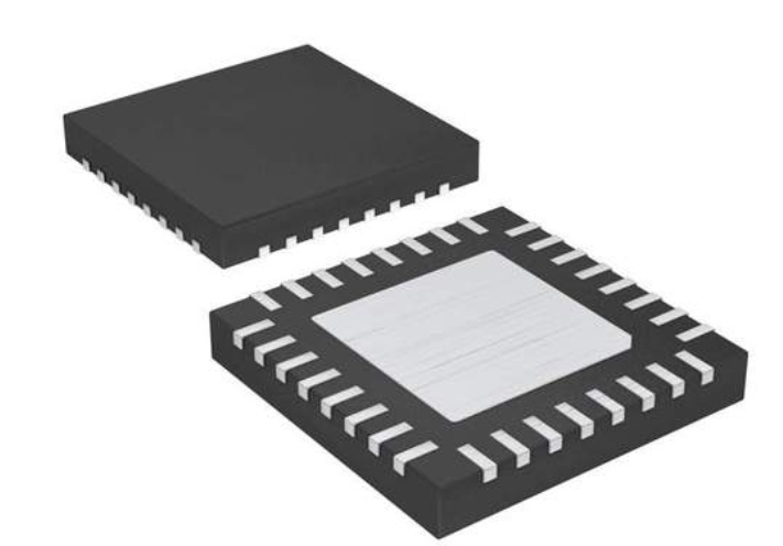


 工商网监
湘ICP备2023018690号
工商网监
湘ICP备2023018690号
