19-0861; Rev 1; 3/10
Fast Dual Driver for ATE with
Waveform Shaping
The MAX9957 dual driver IC for automatic test equipment (ATE) memory applications offers three-level drive
capability, high-speed switching, low timing dispersion,
and features voltage-controlled waveform shaping to
enhance edge-placement accuracy and minimize distortion. It also provides tight matching of gain and offset. The MAX9957 buffers reference voltage inputs for
each channel with nominal -1V to +3.5V voltage ranges.
High-speed differential control inputs, compatible with
CML levels, are provided for each channel. Static
power dissipation is only 1500mW per channel with
nominal -5V and +7V supplies. The MAX9957 power
dissipation at 2Gbps toggling is only 1550mW/channel.
The MAX9957D power dissipation at 2.4Gbps is only
1850mW/channel.
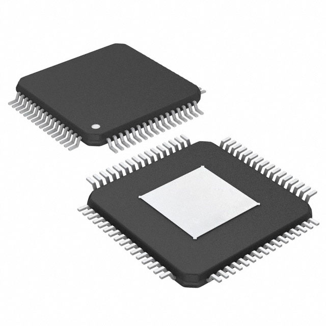
The MAX9957 is available in a 10mm x 10mm x 1mm,
64-pin TQFP package with an exposed pad, inverted
die pad for ease of heat removal.
Applications
Automatic Test Equipment
DDR2 Memory Testers
GDDR3
GDDR4
Features
o Terminator/3-Level Driver
o 2Gbps Toggling at 2VP-P (MAX9957)
o 2.4Gbps Toggling at 2VP-P (MAX9957D)
o Voltage-Controlled Waveform Shaping
o Interfaces Easily With Most Logic Families
o Low Timing Dispersion
Ordering Information
PART
TEMP RANGE
PIN-PACKAGE
MAX9957CCB-D
0°C to +70°C
64 TQFP-EPR*
MAX9957CCB+D
0°C to +70°C
64 TQFP-EPR*
MAX9957DCCB+D
0°C to +70°C
64 TQFP-EPR*
-Denotes a package containing lead(Pb).
D = Dry pack.
+Denotes a lead(Pb)-free/RoHS-compliant package.
*EPR = Exposed pad reversed (exposed pad on top of device).
Pin Configuration
Typical Operating Circuit
BUFFER
DOVS_
DOVL_
ONE OF TWO CHANNELS SHOWN
MAX9955
DUT_
DTV_
VEE
VCC
GND
DHV1
DLV1
DTV1
DOVS1
DOVL1
VL
VCC
GND
1
48 VEE
2
47 GND
GND
3
46 NDATA1
VCC
4
45 DATA1
VEE
5
44 DTERM1
DUT1
6
43 NRCV1
VEE
7
42 RCV1
VCC
8
VCC
9
CH_
DUT2 11
CL_
VCC
VEE
VCC
VEE 10
DROOP
COMPENSATION
VEE
64 63 62 61 60 59 58 57 56 55 54 53 52 51 50 49
I/O
CHV_
NCH_
OVL
DDR3
MEMORY
DUT_
41 RTERM1
MAX9957
40 RTERM2
39 RCV2
38 NRCV2
VEE 12
37 DTERM2
VCC 13
36 DATA2
GND 14
35 NDATA2
VCC 15
34 GND
VEE 16
33 VEE
ONE OF TWO CHANNELS SHOWN
VEE
VCC
GND
DLV2
DHV2
DTV2
DOVS2
DOVL2
RST
VCC
GND
VEE
VCC
GND
CLV_
COS_
COL_
GND
17 18 19 20 21 22 23 24 25 26 27 28 29 30 31 32
NCL_
TEMP
DTV_
DLV_
WAVE
SHAPING
GND
MAX9957
DHV_
INPUT
MUX
GND
TOP VIEW
TQFP-EPR
10mm × 10mm × 1mm
________________________________________________________________ Maxim Integrated Products
For pricing, delivery, and ordering information, please contact Maxim Direct at 1-888-629-4642,
or visit Maxim’s website at www.maxim-ic.com.
1
MAX9957
General Description
�MAX9957
Fast Dual Driver for ATE with
Waveform Shaping
ABSOLUTE MAXIMUM RATINGS
VCC to GND ..............................................................-0.3V to +8V
VEE to GND...............................................................-6V to +0.3V
VCC - VEE ................................................................-0.3V to +14V
VL to GND..............................................................-0.3V to +4.1V
DUT_ to GND............................................................-2V to +4.5V
DATA_, NDATA_, RCV_, NRCV_ to GND ................-0.3V to 4.1V
DATA_ to NDATA_, RCV_ to NRCV_ ..................................±1.5V
VDTERM_ - VDATA_ ....................................................+2V to -0.3V
VDTERM_ - VNDATA_ ..................................................+2V to -0.3V
VRTERM_ - VRCV_ ......................................................+2V to -0.3V
VRTERM_ - VNRCV_ ....................................................+2V to -0.3V
DTERM_, RTERM_ to GND....................................-0.3V to +4.1V
RST to GND...................................................-0.3V to (VL + 0.3V)
DHV_, DLV_, DTV_ to GND (MAX9957) ...................-2V to +4.5V
DHV_, DLV_, DTV_ to GND (MAX9957D)..............-1.7V to +4.5V
DOVS_, DOVL_ to GND.........................................-0.3V to +4.1V
OVL to GND ..................................................-0.3V to (VL + 0.3V)
All Other Pins to GND ......................(VEE - 0.3V) to (VCC + 0.3V)
TEMP Current...................................................-0.5mA to +20mA
DUT_ Current ....................................................-80mA to +80mA
DUT_ Short Circuit to -1V to +3.5V.............................Continuous
Package Power Dissipation (TA = +70°C)
64-Pin TQFP-EP-IDP (derate 125mW/°C above +70°C) ...10W
Storage Temperature Range ............................ -65°C to +150°C
Junction Temperature ......................................................+125°C
Lead Temperature (soldering, 10s) .................................+300°C
Stresses beyond those listed under “Absolute Maximum Ratings” may cause permanent damage to the device. These are stress ratings only, and functional
operation of the device at these or any other conditions beyond those indicated in the operational sections of the specifications is not implied. Exposure to
absolute maximum rating conditions for extended periods may affect device reliability.
ELECTRICAL CHARACTERISTICS
(VCC = +7V, VEE = -5V, VL = +3.3V, VRTERM_ = VDTERM_ = +3.3V, VDHV_ = +2V, VDLV_ = 0V, VDTV_ = +1V, VDOVS_ = VDOVL_ = 0V,
TJ = +70°C ±10°C, unless otherwise noted. All temperature coefficients are measured at TJ = +50°C to +90°C.)
PARAMETER
SYMBOL
CONDITIONS
MIN
TYP
MAX
UNITS
-1.0
+3.5
V
0.1
4.0
V
DC CHARACTERISTICS (Note 1)
Voltage Range
Voltage Swing
Gain
(Note 2)
Gain Temperature Coefficient
Offset
2
DHV:
VDHV_ = 0 and 2.5V, VDLV_ = -1V, VDTV_ = 1.5V
0.997
1.000
1.003
DTV:
VDTV_ = 0 and 2.5V, VDLV_ = -1V, VDHV_ = 3.5V
0.997
1.000
1.003
DLV:
VDHV_ = 3.5V, VDLV_ = 0 and 2.5V, VDTV_ = 1.5V
0.997
1.000
1.003
DHV:
VDHV_ = 0 and 2.5V, VDLV_ = -1V, VDTV_ = 1.5V
-70
DTV:
VDTV_ = 0 and 2.5V, VDLV_ = -1V, VDHV_ = 3.5V
-60
DLV:
VDHV_ = 3.5V, VDLV_ = 0 and 2.5V, VDTV_ = 1.5V
-70
ppm/°C
DHV:
VDHV_ = 2V, VDLV_ = -1V, VDTV_ = 1.5V
±20
DTV:
VDHV_ = 3.5V, VDLV_ = -1V, VDTV_ = 1V
±20
DLV:
VDHV_ = 3.5V, VDLV_ = 0V, VDTV_ = 1.5V
±20
_______________________________________________________________________________________
V/V
mV
�Fast Dual Driver for ATE with
Waveform Shaping
(VCC = +7V, VEE = -5V, VL = +3.3V, VRTERM_ = VDTERM_ = +3.3V, VDHV_ = +2V, VDLV_ = 0V, VDTV_ = +1V, VDOVS_ = VDOVL_ = 0V,
TJ = +70°C ±10°C, unless otherwise noted. All temperature coefficients are measured at TJ = +50°C to +90°C.)
PARAMETER
Offset Temperature Coefficient
SYMBOL
CONDITIONS
MIN
TYP
DHV:
VDHV_ = 2V, VDLV_ = -1V, VDTV_ = 1.5V
-100
DTV:
VDHV_ = 3.5V, VDLV_ = -1V, VDTV_ = 1V
-40
DLV:
VDHV_ = 3.5V, VDLV_ = 0V, VDTV_ = 1.5V
+60
DHV:
VDLV_ = -1V, VDHV_ / VDUT_ = 3.50V / 1.25V,
and 1.25V / 3.50V
MAX
UNITS
µV/°C
±40
DC Output Current
mA
DC Output Resistance
DC Output Resistance Variation
DLV:
VDHV_ = 3.5V, VDLV_ / VDUT_ = +1.25V / -1V
and -1V / +1.25V
±40
IDUT_ = ±20mA, VDUT_ = VDHV_ = 1.25V (Note 3)
48
50
52
IDUT_ = ±1mA, ±8mA; VDUT_ = VDHV_ = 1.25V
0.3
1.0
MAX9957
IDUT_ = ±1mA, ±8mA, ±15mA,
±40mA; VDUT_ = VDHV_ = 1.25V MAX9957D
1.1
2.0
1.5
3.0
Ω
Ω
DHV:
VDHV_ = -1V to +3.5V, VDLV_ = -1V,
VDTV_ = 1.5V
±15
DTV:
VDHV_ = 3.5V, VDLV_ = -1V, VDTV_ = -1V to
+3.5V
±15
DLV:
VDHV_ = 3.5V, VDLV_ = -1V to +3.5V,
VDTV_ = 1.5V
±15
Power-Supply Rejection Ratio
(Note 4)
±18
mV/V
DC Crosstalk
(Note 5)
±5
mV
Linearity Error
(Note 2)
mV
AC CHARACTERISTICS (ZL = 50Ω) (Notes 6, 7)
Prop Delay, Data to Output
VDHV_ = 2V, VDLV_ = 0V
(Note 12)
MAX9957
0.75
1.00
1.25
MAX9957D
0.55
0.80
1.05
Prop-Delay Temperature
Coefficient
+0.85
ns
ps/°C
Prop Delay Match, TLH to THL
VDHV_ = 2V, VDLV_ = 0V (Note 12)
±100
ps
Prop Delay Skew, Channel-toChannel
Same edges (LH and HL)
±50
ps
Prop Delay Change Versus Pulse
Width
2VP-P, 40MHz, 0.5ns to 24.5ns pulse width,
relative to 12.5ns pulse width
±15
ps
Prop Delay Change Versus
Common-Mode Voltage
1VP-P, VDLV_ = -0.5V to +2V, relative to
VDLV_ = 0.75V
±10
ps
_______________________________________________________________________________________
3
MAX9957
ELECTRICAL CHARACTERISTICS (continued)
�MAX9957
Fast Dual Driver for ATE with
Waveform Shaping
ELECTRICAL CHARACTERISTICS (continued)
(VCC = +7V, VEE = -5V, VL = +3.3V, VRTERM_ = VDTERM_ = +3.3V, VDHV_ = +2V, VDLV_ = 0V, VDTV_ = +1V, VDOVS_ = VDOVL_ = 0V,
TJ = +70°C ±10°C, unless otherwise noted. All temperature coefficients are measured at TJ = +50°C to +90°C.)
PARAMETER
SYMBOL
CONDITIONS
MIN
TYP
MAX
MAX9957
0.73
0.98
1.23
MAX9957D
0.63
0.88
1.13
UNITS
Prop Delay, Data to Term and
Term to Data
(Note 12)
Rise/Fall Time, 1V
VDHV_ = 1V, VDTV_ = 0.5V,
VDLV_ = 0V, 20% to 80%
MAX9957
80
130
180
MAX9957D
70
120
160
Rise/Fall Time, 2V
VDHV_ = 2V, VDTV_ = 1V,
VDLV_ = 0V, 20% to 80%
MAX9957
100
150
200
MAX9957D
100
140
190
Minimum Pulse Width, 1V
VDHV_ = 1V, VDLV_ = 0V, time to
reach 95% amplitude (Note 12)
MAX9957
350
450
MAX9957D
270
370
Minimum Pulse Width, 2V
VDHV_ = 2V, VDLV_ = 0V, time to
reach 95% amplitude (Note 12)
MAX9957
400
500
MAX9957D
300
400
Overshoot
0.5V to 2V swing (Notes 8 and 9)
Input Voltage Range,
DOVS_/DOVL_
0V = no peaking, 3.3V = 25% peaking
Undershoot
0.5V to 2V swing (Note 9)
1
%
Output Return Loss By TDR
Drive amplitude = 1V, VDLV_ = 0V, VDHV_ =
1V, rise time = 150ps (10% to 90%) (Note 10)
5
%
(4% to
25%) +
25
0
ns
ps
ps
ps
ps
mV
3.3
V
DIFFERENTIAL CONTROL INPUTS (DATA_, NDATA_, RCV_, and NRCV_)
Input High Voltage
1.0
3.6
Input Low Voltage
0.8
3.4
V
±0.2
±1.0
V
0
1.9
V
Input Termination Voltage
1.7
3.6
V
Input Termination Resistor
48
52
Ω
±25
µA
Differential Input Voltage
Voltage Between a Differential
Input and its Termination
50
V
SINGLE-ENDED INPUTS (DLV_, DHV_, DTV_, DOVS_, and DOVL_)
Input Bias Current
SINGLE-ENDED INPUT (RST)
Input High Voltage
1.65
3.50
V
Input Low Voltage
-0.10
+0.85
V
±50
µA
3.60
V
2.0
mA
VL
V
Input Bias Current
SINGLE-ENDED OUTPUT (OVL) (Note 7)
Digital Supply Voltage
VL
Digital Supply Current
IL
Output High Voltage
4
3.00
No load
Load current = -1mA
0.5
1.0
VL - 0.4
_______________________________________________________________________________________
�Fast Dual Driver for ATE with
Waveform Shaping
(VCC = +7V, VEE = -5V, VL = +3.3V, VRTERM_ = VDTERM_ = +3.3V, VDHV_ = +2V, VDLV_ = 0V, VDTV_ = +1V, VDOVS_ = VDOVL_ = 0V,
TJ = +70°C ±10°C, unless otherwise noted. All temperature coefficients are measured at TJ = +50°C to +90°C.)
PARAMETER
SYMBOL
CONDITIONS
Output Low Voltage
Load current = 1mA
Rise/Fall Time
10% to 90% (Note 11)
Overcurrent Detect Threshold
(Note 12)
MIN
TYP
0
MAX
0.4
3.6
±50
UNITS
V
ns
±80
mA
TEMPERATURE MONITOR
Nominal Voltage
TJ = +70°C, RL > 10MΩ
3.43
Temperature Coefficient
V
+10
Output Resistance
mV/°C
17
23
29
kΩ
V
POWER SUPPLIES
Positive Voltage Range
VCC
Positive Supply Current
ICC
Negative Voltage Range
VEE
Negative Supply Current
IEE
Static Power Dissipation
fOUT = 0Gbps
Operating Power Dissipation
fOUT = 2Gbps, 2VP-P
Note 1:
Note 2:
Note 3:
Note 4:
Note 5:
Note 6:
Note 7:
Note 8:
Note 9:
6.75
7.00
7.50
MAX9957
204
222
240
MAX9957D
245
265
285
-5.50
-5.00
-4.75
MAX9957
260
283
306
MAX9957D
295
330
360
MAX9957
2.4
3.0
3.6
MAX9957D
3.05
3.5
4.15
MAX9957
3.1
MAX9957D
3.7
mA
V
mA
W
W
RL ≥ 10MΩ, unless otherwise noted. All specifications apply to DHV, DLV, and DTV.
Relative to a straight line through 0 and 2.5V.
Other values of DC output resistance are available on request, contact factory; 45Ω to 51Ω.
Change in offset voltage with power supplies independently set to their minimum and maximum values.
DC crosstalk is to be measured under six different conditions shown below with the worst case reported:
1) DTV to DHV: VDHV_ = 3.5V, VDLV_ = 3.4V, VDTV_ = -1V to +3.5V (Driver Output: DHV)
2) DTV to DLV: VDHV_ = -0.9V, VDLV_ = -1V, VDTV_ = -1V to +3.5V (Driver Output: DLV)
3) DHV to DLV: VDTV_ = -1V, VDLV_ = -1V, VDHV_ = -0.9V to +3.5V (Driver Output: DLV)
4) DHV to DTV: VDTV_ = -1V, VDLV_ = -1V, VDHV_ = -0.9V to +3.5V (Driver Output: DTV)
5) DLV to DHV: VDHV_ = 3.5V, VDTV_ = 3.5V, VDLV_ = -1V to +3.4V (Driver Output: DHV)
6) DLV to DTV: VDHV_ = 3.5V, VDTV_ = 3.5V, VDLV_ = -1V to +3.4V (Driver Output: DTV)
Load is a terminated 3ns, 50Ω transmission line with 50Ω external termination resistor to GND, unless otherwise specified.
Propagation delays are measured from the crossing point of the differential input signals to the 50% point of the expected
output swing. Rise time of the differential inputs DATA_ and RCV_ is 300ps (10% to 90%).
Guaranteed by design.
Driver overshoot setting and output waveform. The voltage range of DOVS_, DOVL_ is 0 to +3.3V, 0 is for no overshoot,
and +3.3V is for 25% overshoot, respectively. The fall time of overshoot for DOVS_ (90% to 10%) is 77ps, the fall time of
overshoot for DOVL_ (90% to 10%) is 1.5ns.
The definitions of overshoot and undershoot are detailed in this figure:
OVERSHOOT
UNDERSHOOT
UNDERSHOOT
OVERSHOOT
_______________________________________________________________________________________
5
MAX9957
ELECTRICAL CHARACTERISTICS (continued)
�Note 10: The definition of output return loss by time domain reflectometry (TDR) is: output return loss = (reflection amplitude / drive
amplitude) x 100 (%), with terms defined in this figure:
REFLECTION
AMPLITUDE
DRIVE
AMPLITUDE
tR
Note 11: Timing characteristics with VL = 3.3V.
Note 12: Guaranteed by design. Not production tested.
Typical Operating Characteristics (MAX9957)
(VCC = +7V, VEE = -5V, VL = +3.3V, VRTERM_ = VDTERM_ = +3.3V, VDHV_ = +2V, VDLV_ = 0V, VDTV_ = +1V, VDOVS_ = VDOVL_ = 0V,
TJ = +70°C ±10°C, unless otherwise noted. All temperature coefficients are measured at TJ = +50°C to +90°C.)
VDHV_ = 0.5V
VDHV_ = 0.3V
MAX9957 toc03
VDLV_ = 0V, VDHV_ = 1V, RL = 50Ω,
VDOVL_ = 0V, VDOVS_ = 0V
VDUT_ = 100mV/div
VDHV_ = 0.7V
VDLV_ = 0V,
RL = 50Ω,
VDOVL_ = 0V,
VDOVS_ = 0V
MAX9957 toc02
VDHV_ = 3V
VDUT_ = 200mV/div
VDUT_ = 100mV/div
VDLV_ = 0V, RL = 50Ω,
VDOVL_ = 0V, VDOVS_ = 0V
DRIVER 1V, 2Gbps SIGNAL RESPONSE
DRIVER LARGE-SIGNAL RESPONSE
MAX9957 toc01
DRIVER SMALL-SIGNAL RESPONSE
VDHV_ = 2V
VDHV_ = 1V
0V
0V
t = 200ps/div
DRIVER 1V, 3Gbps SIGNAL RESPONSE
DRIVER 2V, 2Gbps SIGNAL RESPONSE
DRIVER 3V, 1Gbps SIGNAL RESPONSE
VDUT_ = 300mV/div
VDLV_ = 0V, VDHV_ = 3V, RL = 50Ω,
VDOVL_ = 0V, VDOVS_ = 0V
0V
0V
0V
t = 200ps/div
6
VDLV_ = 0V, VDHV_ = 2V, RL = 50Ω,
VDOVL_ = 0V, VDOVS_ = 0V
VDUT_ = 200mV/div
VDLV_ = 0V, VDHV_ = 1V, RL = 50Ω,
VDOVL_ = 0V, VDOVS_ = 0V
MAX9957 toc05
t = 2ns/div
MAX9957 toc04
t = 2ns/div
t = 200ps/div
t = 250ps/div
_______________________________________________________________________________________
MAX9957 toc06
0V
VDUT_ = 100mV/div
MAX9957
Fast Dual Driver for ATE with
Waveform Shaping
�Fast Dual Driver for ATE with
Waveform Shaping
MAX9957 toc08
MAX9957 toc07
VDLV_ = 0V
VDHV_ = 2V
VDOVL_ = 0V
RL = 50Ω
VDUT_ = 50mV/div
VDUT_ = 50mV/div
VDOVS_ = 1V
VDOVS_ = 0V
VDOVS_ = 0V
VDOVS_ = 1V
VDLV_ = 0V
VDHV_ = 2V
VDOVL_ = 0V
RL = 50Ω
VDOVS_ = 2V
1V
VDLV_ = 0V
VDHV_ = 2V
VDOVS_ = 0V
RL = 50Ω
VDOVL_ = 3V
0V
VDOVS_ = 2V
VDUT_ = 50mV/div
VDOVS_ = 3V
DRIVER SIGNAL RESPONSE
WITH DRIVER OVERSHOOT
MAX9957 toc09
DRIVER SIGNAL RESPONSE
WITH DRIVER OVERSHOOT
DRIVER SIGNAL RESPONSE
WITH DRIVER OVERSHOOT
VDOVL_ = 2V
VDOVL_ = 1V
VDOVL_ = 0V
1V
VDOVS_ = 3V
DRIVER SIGNAL RESPONSE
WITH DRIVER OVERSHOOT
DRIVER OVERSHOOT
vs. DOVS_ VOLTAGE
DRIVER OVERSHOOT
vs. DOVL_ VOLTAGE
VDOVL_ = 1V
VDOVL_ = 2V
VDLV_ = 0V
VDHV_ = 2V
VDOVS_ = 0V
RL = 50Ω
VDOVL_ = 3V
0.20
0.18
0.16
FALL
0.14
0.12
0.10
RISE
0
-5
-10
FALL
-15
-20
1.0
1.5
2.0
2.5
3.0
0
5
10
15
PULSE WIDTH (ns)
20
25
0.5
1.0
1.5
2.0
2.5
3.0
VDOVL_ (V)
DRIVER 2V TRAILING EDGE
ERROR vs. PULSE WIDTH
DRIVER TIME DELAY
vs. COMMON-MODE VOLTAGE
15
MAX9957 toc14
VDLV_ = 0V
VDHV_ = 2V
RL = 50Ω
10
0
VDOVS_ (V)
5
0
-5
RISE
-10
FALL
-15
RL = 50Ω
10
5
3.5
RISE
0
-5
FALL
-10
-20
-25
-25
RISE
0.10
3.5
DRIVER TIME DELAY (ps)
5
FALL
0.12
0.04
0.5
15
DRIVER 2V TRAILING EDGE ERROR (ps)
RISE
0.14
0.06
0
MAX9957 toc13
DRIVER 2V TRAILING EDGE ERROR (ps)
VDLV_ = 0V
VDHV_ = 2V
RL = 50Ω
0.16
0.06
DRIVER 2V TRAILING EDGE
ERROR vs. PULSE WIDTH
10
0.18
0.08
t = 500ps/div
VDLV_ = 0V
VDHV_ = 2V
VDOVS_ = 0V
RL = 50Ω
0.20
0.08
0.04
15
0.28
0.26
0.24
0.22
MAX9957 toc15
VDOVL_ = 0V
VDLV_ = 0V
VDHV_ = 2V
VDOVL_ = 0V
RL = 50Ω
DRIVER OVERSHOOT (V)
DRIVER OVERSHOOT (V)
VDUT_ = 50mV/div
0V
0.28
0.26
0.24
0.22
MAX9957 toc12
t = 500ps/div
MAX9957 toc11
t = 250ps/div
MAX9957 toc10
t = 250ps/div
-15
0.5
1.0
1.5
2.0
2.5
3.0
PULSE WIDTH (ns)
3.5
4.0
4.5
-0.5
0
0.5
1.0
1.5
2.0
2.5
3.0
COMMON-MODE VOLTAGE (V)
_______________________________________________________________________________________
7
MAX9957
Typical Operating Characteristics (MAX9957) (continued)
(VCC = +7V, VEE = -5V, VL = +3.3V, VRTERM_ = VDTERM_ = +3.3V, VDHV_ = +2V, VDLV_ = 0V, VDTV_ = +1V, VDOVS_ = VDOVL_ = 0V,
TJ = +70°C ±10°C, unless otherwise noted. All temperature coefficients are measured at TJ = +50°C to +90°C.)
�Typical Operating Characteristics (MAX9957) (continued)
(VCC = +7V, VEE = -5V, VL = +3.3V, VRTERM_ = VDTERM_ = +3.3V, VDHV_ = +2V, VDLV_ = 0V, VDTV_ = +1V, VDOVS_ = VDOVL_ = 0V,
TJ = +70°C ±10°C, unless otherwise noted. All temperature coefficients are measured at TJ = +50°C to +90°C.)
DRIVER LINEARITY ERROR
vs. OUTPUT VOLTAGE
0V
2.5
0
-0.5
-1.0
2.0
1.5
0.5
-1.0 -0.5
CROSSTALK TO DUT
FROM DLV WITH DUT = DTV
CROSSTALK TO DUT
FROM DHV WITH DUT = DTV
VDHV_ = 3.5V
VDTV_ = 3.5V
RL = OPEN
1.0
0.5
0
-0.5
2.5
1.5
1.0
0.5
0
-0.5
-1.0
-1.0
-1.5
-1.5
-1.0
-2.0
-2.0
-1.5
-2.5
-2.5
0
0.5 1.0 1.5 2.0 2.5 3.0 3.5
VDLV_ (V)
CROSSTALK TO DUT
FROM DTV WITH DUT = DHV
CROSSTALK TO DUT
FROM DTV WITH DUT = DLV
1.5
2.5
1.5
CROSSTALK (mV)
1.0
0.5
0
-0.5
VDHV_ = -0.9V
VDLV_ = -1V
RL = OPEN
2.0
1.0
2.0
1.5
0.5
0
-0.5
0.5
0
-0.5
-1.0
-1.0
-1.5
-1.5
-2.0
-2.0
-2.0
-2.5
-2.5
0.5 1.0 1.5 2.0 2.5 3.0 3.5
VDTV_ (V)
VDHV_ = 3.5V
VDTV_ = 3.5V
RL = OPEN
1.0
-1.5
0
0.5 1.0 1.5 2.0 2.5 3.0 3.5
VDHV_ (V)
2.5
-1.0
-1.0 -0.5
0
CROSSTALK TO DUT
FROM DLV WITH DUT = DTV
CROSSTALK (mV)
VDHV_ = 3.5V
VDLV_ = 3.4V
RL = OPEN
2.0
-1.0 -0.5
MAX9957 toc23
-1.0 -0.5
VDTV_ (V)
2.5
VDTV_ = -1V
VDLV_ = -1V
RL = OPEN
2.0
0
0.5 1.0 1.5 2.0 2.5 3.0 3.5
0.5 1.0 1.5 2.0 2.5 3.0 3.5
VDLV_ (V)
-0.5
0
0
VDHV_ (V)
CROSSTALK (mV)
CROSSTALK (mV)
1.0
0.5 1.0 1.5 2.0 2.5 3.0 3.5
MAX9957 toc20
MAX9957 toc19
1.5
-1.0 -0.5
8
-1.5
0
2.5
MAX9957 toc22
VDUT_ ERROR (mV)
2.0
0
-1.0
DRIVER LINEARITY ERROR
vs. OUTPUT VOLTAGE
2.5
0.5
-2.0
-1.0 -0.5
VDLV_ = -1V
VDHV_ = 3.5V
RL = OPEN
1.0
-0.5
t = 2ns/div
3.0
1.5
-1.5
-2.5
3.5
2.0
MAX9957 toc21
DLV_ to DTV_
0.5
VDHV_ = 3.5V
VDTV_ = 1.5V
RL = OPEN
3.0
MAX9957 toc18
1.0
3.5
VDUT_ ERROR (mV)
DHV_ to DTV_
VDLV_ = -1V
VDTV_ = 1.5V
RL = OPEN
1.5
MAX9957 toc24
MAX9957 toc16
2.0
VDUT_ ERROR (mV)
VDUT_ = 200mV/div
VDHV_ = 2V, VDTV_ = 1V, VDLV_ = 0V, RL = 50Ω,
VDOVL_ = 0V, VDOVS_ = 0V
DRIVER LINEARITY ERROR
vs. OUTPUT VOLTAGE
MAX9957 toc17
DRIVE-TO-TERM TRANSITION
CROSSTALK (mV)
MAX9957
Fast Dual Driver for ATE with
Waveform Shaping
-2.5
-1.0 -0.5
0
0.5 1.0 1.5 2.0 2.5 3.0 3.5
VDTV_ (V)
-1.0 -0.5
0
0.5 1.0 1.5 2.0 2.5 3.0 3.5
VDLV_ (V)
_______________________________________________________________________________________
�Fast Dual Driver for ATE with
Waveform Shaping
DRIVER GAIN vs. TEMPERATURE
RL = OPEN
1.003
0
-0.5
-1.0
DHV, DTV, DLV
1.001
1.000
0.999
2
1
-1
-2
-2.0
0.997
-3
-2.5
0.996
0.5 1.0 1.5 2.0 2.5 3.0 3.5
55
60
VDHV_ (V)
65
70
75
80
90
50
55
236
232
60
65
70
75
80
85
90
TEMPERATURE (°C)
SUPPLY CURRENT, IEE vs.
SUPPLY VOLTAGE, VEE
-261
MAX9957 toc29
240
-266
-271
-276
228
224
220
-281
-286
-291
216
208
85
TEMPERATURE (°C)
SUPPLY CURRENT, ICC vs.
SUPPLY VOLTAGE, VCC
212
VDLV_ = 0V
-4
50
IEE (mA)
0
MAX9957 toc28
-1.0 -0.5
VDTV_ = 1V
0
0.998
-1.5
VDHV_ = 2V
3
DRIVER OFFSET (mV)
DRIVER GAIN (V/V)
0.5
RL = OPEN
4
1.002
1.0
ICC (mA)
CROSSTALK (mV)
1.5
VDTV_ = -1V
VDLV_ = -1V
RL = OPEN
DRIVER OFFSET vs. TEMPERATURE
5
MAX9957 toc26
2.0
1.004
MAX9957 toc25
2.5
MAX9957 toc27
CROSSTALK TO DUT
FROM DHV WITH DUT = DTV
VDHV1 = VDHV2 = 2V,
VDTV1 = VDTV2 = 1V,
VDLV1 = VDLV2 = 0V,
RL = OPEN
-296
-301
204
6.75
6.85
6.95
7.05
VCC (V)
7.15
7.25
VDHV1 = VDHV2 = 2V,
VDTV1 = VDTV2 = 1V,
VDLV1 = VDLV2 = 0V,
RL = OPEN
-306
-5.50
-5.35
-5.20
-5.05
-4.90
-4.75
VEE (V)
_______________________________________________________________________________________
9
MAX9957
Typical Operating Characteristics (MAX9957) (continued)
(VCC = +7V, VEE = -5V, VL = +3.3V, VRTERM_ = VDTERM_ = +3.3V, VDHV_ = +2V, VDLV_ = 0V, VDTV_ = +1V, VDOVS_ = VDOVL_ = 0V,
TJ = +70°C ±10°C, unless otherwise noted. All temperature coefficients are measured at TJ = +50°C to +90°C.)
�Typical Operating Characteristics (MAX9957D)
(VCC = +7V, VEE = -5V, VL = +3.3V, VRTERM_ = VDTERM_ = +3.3V, VDHV_ = +2V, VDLV_ = 0V, VDTV_ = +1V, VDOVS_ = VDOVL_ = 0V,
TJ = +70°C ±10°C, unless otherwise noted. All temperature coefficients are measured at TJ = +50°C to +90°C.)
VDHV_ = 0.5V
VDHV_ = 0.3V
VDLV_ = 0V, VDHV_ = 1V, RL = 50I
VDUT_ = 100mV/div
VDUT_ = 200mV/div
VDUT_ = 100mV/div
VDHV_ = 0.7V
VDLV_ = 0V,
RL = 50I
VDHV_ = 3V
MAX9957D toc02
MAX9957D toc01
VDLV_ = 0V, RL = 50I
DRIVER 1V, 2.4Gbps
SIGNAL RESPONSE
DRIVER LARGE-SIGNAL RESPONSE
MAX9957D toc03
DRIVER SMALL-SIGNAL RESPONSE
VDHV_ = 2V
VDHV_ = 1V
0V
0V
DRIVER 1V, 3Gbps
SIGNAL RESPONSE
DRIVER 2V, 2.4Gbps
SIGNAL RESPONSE
DRIVER 3V, 1Gbps
SIGNAL RESPONSE
0V
0V
t = 250ps/div
DRIVER SIGNAL RESPONSE
WITH DRIVER OVERSHOOT
DRIVER SIGNAL RESPONSE
WITH DRIVER OVERSHOOT
DRIVER SIGNAL RESPONSE
WITH DRIVER OVERSHOOT
VDOVS_ = 1V
VDOVS_ = 0V
1V
0V
VDOVS_ = 0V
VDOVS_ = 1V
VDOVS_ = 2V
VDOVS_ = 3V
t = 250ps/div
10
t = 250ps/div
VDLV_ = 0V
VDHV_ = 2V
VDOVL_ = 0V
RL = 50I
VDLV_ = 0V
VDHV_ = 2V
VDOVS_ = 0V
RL = 50I
VDOVL_ = 3V
VDUT_ = 50mV/div
VDOVS_ = 2V
VDLV_ = 0V
VDHV_ = 2V
VDOVL_ = 0V
RL = 50I
VDUT_ = 50mV/div
VDOVS_ = 3V
MAX9957D toc08
t = 200ps/div
MAX9957D toc07
t = 200ps/div
VDOVL_ = 2V
VDOVL_ = 1V
VDOVL_ = 0V
1V
t = 500ps/div
______________________________________________________________________________________
MAX9957D toc09
0V
VDLV_ = 0V, VDHV_ = 3V, RL = 50I
VDUT_ = 300mV/div
VDUT_ = 200mV/div
VDUT_ = 100mV/div
VDLV_ = 0V, VDHV_ = 2V, RL = 50I
MAX9957D toc05
t = 200ps/div
MAX9957D toc04
t = 2ns/div
MAX9957D toc06
0V
t = 2ns/div
VDLV_ = 0V, VDHV_ = 1V, RL = 50I
VDUT_ = 50mV/div
MAX9957
Fast Dual Driver for ATE with
Waveform Shaping
�Fast Dual Driver for ATE with
Waveform Shaping
0
t = 500ps/div
10
5
FALL
RISE
0
-5
-10
-15
-20
15
DRIVER 2V TRAILING EDGE ERROR (ps)
1.0
1.5
2.0
2.5
3.0
5
5
10
15
20
0
3.5
0.5
1.0
1.5
2.0
3.0
2.5
DRIVER 2V TRAILING EDGE ERROR
vs. PULSE WIDTH
DRIVER TIME DELAY
vs. COMMON-MODE VOLTAGE
0
FALL
-5
RISE
-10
-15
15
RL = 50I
10
RISE
5
0
-5
FALL
-15
0.5
1.0
1.5
2.0
2.5
3.0
3.5
4.0
4.5
-0.5
0
0.5
1.0
1.5
2.0
2.5
PULSE WIDTH (ns)
PULSE WIDTH (ns)
COMMON-MODE VOLTAGE (V)
DRIVE-TO-TERM TRANSITION
DRIVER LINEARITY ERROR
vs. OUTPUT VOLTAGE
DRIVER LINEARITY ERROR
vs. OUTPUT VOLTAGE
DLV_ TO DTV_
0V
3.5
3.0
2.5
VDLV_ = -1V
VDTV_ = 1.5V
RL = OPEN
VDUT_ ERROR (mV)
DHV_ TO DTV_
4.0
VDUT_ ERROR (mV)
VDHV_ = 2V, VDTV_ = 1V, VDLV_ = 0V, RL = 50I
2.0
1.5
1.0
0.5
0
-0.5
-1.0
-1.5
-2.0
t = 2ns/div
3.5
-10
-20
25
MAX9957D toc16
0
RISE
VDOVL_ (V)
VDLV_ = 0V
VDHV_ = 2V
RL = 50I
10
FALL
VDOVS_ (V)
-25
-25
VDUT_ = 200mV/div
0.5
MAX9957D toc17
DRIVER 2V TRAILING EDGE ERROR (ps)
VDLV_ = 0V
VDHV_ = 2V
RL = 50I
MAX9957D toc13
DRIVER 2V TRAILING EDGE ERROR
vs. PULSE WIDTH
15
MAX9957D toc11
RISE
VDLV_ = 0V
VDHV_ = 2V
VDOVS_ = 0V
RL = 50I
MAX9957D toc15
VDOVL_ = 3V
FALL
0.40
0.38
0.36
0.34
0.32
0.30
0.28
0.26
0.24
0.22
0.20
0.18
0.16
0.14
0.12
0.10
0.08
0.06
-1.0 -0.5
0
0.5 1.0 1.5 2.0 2.5 3.0 3.5
VDHV_ (V)
4.5
4.0
3.5
3.0
2.5
2.0
1.5
1.0
0.5
0
-0.5
-1.0
-1.5
-2.0
-2.5
-3.0
VDHV_ = 3V
VDTV_ = 1.5V
RL = OPEN
-1.0 -0.5
0
3.0
MAX9957D toc18
VDLV_ = 0V
VDHV_ = 2V
VDOVS_ = 0V
RL = 50I
OVERSHOOT (V)
VDOVL_ = 1V
VDLV_ = 0V
VDHV_ = 2V
VDOVL_ = 0V
RL = 50I
DRIVER TIME DELAY (ps)
OVERSHOOT (V)
VDOVL_ = 0V
0.40
0.38
0.36
0.34
0.32
0.30
0.28
0.26
0.24
0.22
0.20
0.18
0.16
0.14
0.12
0.10
0.08
0.06
MAX9957D toc14
MAX9957D toc10
VDUT_ = 50mV/div
0V
VDOVL_ = 2V
DRIVER OVERSHOOT
vs. DOVL_ VOLTAGE
DRIVER OVERSHOOT
vs. DOVS_ VOLTAGE
MAX9957D toc12
DRIVER SIGNAL RESPONSE
WITH DRIVER OVERSHOOT
0.5 1.0 1.5 2.0 2.5 3.0 3.5
VDLV_ (V)
______________________________________________________________________________________
11
MAX9957
Typical Operating Characteristics (MAX9957D) (continued)
(VCC = +7V, VEE = -5V, VL = +3.3V, VRTERM_ = VDTERM_ = +3.3V, VDHV_ = +2V, VDLV_ = 0V, VDTV_ = +1V, VDOVS_ = VDOVL_ = 0V,
TJ = +70°C ±10°C, unless otherwise noted. All temperature coefficients are measured at TJ = +50°C to +90°C.)
�Typical Operating Characteristics (MAX9957D) (continued)
(VCC = +7V, VEE = -5V, VL = +3.3V, VRTERM_ = VDTERM_ = +3.3V, VDHV_ = +2V, VDLV_ = 0V, VDTV_ = +1V, VDOVS_ = VDOVL_ = 0V,
TJ = +70°C ±10°C, unless otherwise noted. All temperature coefficients are measured at TJ = +50°C to +90°C.)
MAX9957D toc20
VDHV_ = 3.5V
VDTV_ = 3.5V
RL = OPEN
1.0
0.5
0
-0.5
-1.5
-2.0
-2.5
0.5 1.0 1.5 2.0 2.5 3.0 3.5
-1.0 -0.5
0
0.5 1.0 1.5 2.0 2.5 3.0 3.5
VDTV_ (V)
VDLV_ (V)
CROSSTALK TO DUT
FROM DHV WITH DUT = DLV
CROSSTALK TO DUT
FROM DTV WITH DUT = DHV
1.5
2.5
MAX9957D toc21
VDTV_ = -1V
VDLV_ = -1V
RL = OPEN
2.0
1.5
CROSSTALK (mV)
1.0
0.5
0
-0.5
1.0
0.5
0
-0.5
-1.0
-1.0
-1.5
-1.5
-2.0
-2.0
-2.5
-2.5
-1.0 -0.5
0
VDHV_ = 3.5V
VDLV_ = 3.4V
RL = OPEN
2.0
0.5 1.0 1.5 2.0 2.5 3.0 3.5
-1.0 -0.5
0
0.5 1.0 1.5 2.0 2.5 3.0 3.5
VDTV_ (V)
CROSSTALK TO DUT
FROM DTV WITH DUT = DLV
CROSSTALK TO DUT
FROM DLV WITH DUT = DTV
VDHV_ = -0.9V
VDLV_ = -1V
RL = OPEN
2.0
1.5
2.5
1.5
CROSSTALK (mV)
1.0
2.0
0.5
0
-0.5
0.5
0
-0.5
-1.0
-1.5
-1.5
-2.0
-2.0
-2.5
-2.5
0
0.5 1.0 1.5 2.0 2.5 3.0 3.5
VDTV_ (V)
VDHV_ = 3.5V
VDTV_ = 3.5V
RL = OPEN
1.0
-1.0
-1.0 -0.5
MAX9957D toc24
VDHV_ (V)
2.5
MAX9957D toc22
0
2.5
CROSSTALK (mV)
1.5
-1.0
-1.0 -0.5
12
2.5
2.0
CROSSTALK (mV)
VDLV_ = -1V
VDHV_ = 3.5V
RL = OPEN
MAX9957D toc19
4.5
4.0
3.5
3.0
2.5
2.0
1.5
1.0
0.5
0
-0.5
-1.0
-1.5
-2.0
-2.5
CROSSTALK TO DUT
FROM DLV WITH DUT = DTV
MAX9957D toc23
VDUT_ ERROR (mV)
DRIVER LINEARITY ERROR
vs. OUTPUT VOLTAGE
CROSSTALK (mV)
MAX9957
Fast Dual Driver for ATE with
Waveform Shaping
-1.0 -0.5
0
0.5 1.0 1.5 2.0 2.5 3.0 3.5
VDLV_ (V)
______________________________________________________________________________________
�Fast Dual Driver for ATE with
Waveform Shaping
CROSSTALK TO DUT
FROM DHV WITH DUT = DTV
1.5
RL = OPEN
1.008
1.006
1.004
DRIVER GAIN (V/V)
1.0
0.5
0
-0.5
1.002
1.000
0.998
-1.0
0.996
-1.5
0.994
-2.0
0.992
0.990
-2.5
0
50
0.5 1.0 1.5 2.0 2.5 3.0 3.5
55
65
70
75
80
85
90
SUPPLY CURRENT, ICC
vs. SUPPLY VOLTAGE, VCC
DRIVER OFFSET vs. TEMPERATURE
RL = OPEN
4
VDHV_ = 2V
280
MAX9957D toc27
5
3
60
TEMPERATURE (°C)
VDHV_ (V)
276
MAX9957D toc28
-1.0 -0.5
VDHV1 = VDHV2 = 2V
VDTV1 = VDTV2 = 1V
VDLV1 = VDLV2 = 0V
RL = OPEN
1
ICC (mA)
2
VDTV_ = 1V
0
272
268
-1
VDLV_ = 0V
-2
264
-3
260
-4
50
55
60
65
70
75
80
6.75
90
85
6.85
6.95
7.05
7.15
7.25
VCC (V)
TEMPERATURE (°C)
SUPPLY CURRENT, IEE
vs. SUPPLY VOLTAGE, VEE
-319
MAX9957D toc29
-315
IEE (mA)
DRIVER OFFSET (mV)
MAX9957D toc26
VDTV_ = -1V
VDLV_ = -1V
RL = OPEN
2.0
CROSSTALK (mV)
DRIVER GAIN vs. TEMPERATURE
1.010
MAX9957D toc25
2.5
VDHV1 = VDHV2 = 2V
VDTV1 = VDTV2 = 1V
VDLV1 = VDLV2 = 0V
RL = OPEN
-323
-327
-331
-335
-5.50
-5.35
-5.20
-5.05
-4.90
-4.75
VEE (V)
______________________________________________________________________________________
13
MAX9957
Typical Operating Characteristics (MAX9957D) (continued)
(VCC = +7V, VEE = -5V, VL = +3.3V, VRTERM_ = VDTERM_ = +3.3V, VDHV_ = +2V, VDLV_ = 0V, VDTV_ = +1V, VDOVS_ = VDOVL_ = 0V,
TJ = +70°C ±10°C, unless otherwise noted. All temperature coefficients are measured at TJ = +50°C to +90°C.)
�MAX9957
Fast Dual Driver for ATE with
Waveform Shaping
Pin Description
PIN
NAME
1, 5, 7, 10,
12, 16, 20,
32, 33, 48,
49, 61
VEE
Negative Power Supply
2, 4, 8, 9, 13,
15, 21, 23,
31, 50, 58,
60
VCC
Positive Power Supply
3, 14, 17, 19,
22, 30, 34,
47, 51, 59,
62, 64
GND
Ground
14
FUNCTION
6
DUT1
Driver 1 Output
11
DUT2
Driver 2 Output
18
TEMP
Temperature Monitor Output
24
RST
Reset Input. Reset for the overcurrent detector. Clears the OVL output.
25
DOVL2
Driver Overshoot Voltage-Control Input, Long. Setting for DC waveform shaping for long-term
overshoot of channel 2.
26
DOVS2
Driver Overshoot Voltage-Control Input, Short. Setting for DC waveform shaping for short-term
overshoot of channel 2.
27
DTV2
Driver Term Voltage Input. DC input voltage for channel 2.
28
DHV2
Driver High Voltage Input. DC input voltage for channel 2.
29
DLV2
Driver Low Voltage Input. DC input voltage for channel 2.
35
NDATA2
Multiplexer 2 Data Negative Control Input. NDATA and DATA form the differential multiplexer inputs
that select between DHV and DLV for channel 2.
36
DATA2
Multiplexer 2 Data Positive Control Input. DATA and NDATA form the differential multiplexer inputs
that select between DHV and DLV for channel 2.
37
DTERM2
Data Termination 2 Voltage Input. Termination voltage connection for DATA/NDATA input termination
resistors of channel 2.
38
NRCV2
Multiplexer 2 Receive Negative Control Input. NRCV and RCV form the differential multiplexer inputs
that select between DTV and DHV/DLV for channel 2.
39
RCV2
Multiplexer 2 Receive Positive Control Input. RCV and NRCV form the differential multiplexer inputs
that select between DTV and DHV/DLV for channel 2.
40
RTERM2
Receive Termination 2 Voltage Input. Termination voltage connection for channel 2 RCV/NRCV input
termination resistors.
41
RTERM1
Receive Termination 1 Voltage Input. Termination voltage connection for channel 1 RCV/NRCV input
termination resistors.
42
RCV1
Multiplexer 1 Receive Positive Control Input. RCV and NRCV form the differential multiplexer inputs
that select between DTV and DHV/DLV for channel 1.
43
NRCV1
Multiplexer 1 Receive Negative Control Input. NRCV and RCV form the differential multiplexer inputs
that select between DTV and DHV/DLV for channel 1.
______________________________________________________________________________________
�Fast Dual Driver for ATE with
Waveform Shaping
PIN
NAME
FUNCTION
Data Termination 1 Voltage Input. Termination voltage connection for DATA/NDATA input termination
resistors of channel 1.
44
DTERM1
45
DATA1
Multiplexer 1 Data Positive Control Input. DATA and NDATA form the differential multiplexer inputs
that select between DHV and DLV for channel 1.
46
NDATA1
Multiplexer 1 Data Negative Control Input. NDATA and DATA form the differential multiplexer inputs
that select between DHV and DLV for channel 1.
52
DLV1
53
DHV1
Driver High Voltage Input. DC input voltage for channel 1.
54
DTV1
Driver Term Voltage Input. DC input voltage for channel 1.
55
DOVS1
Driver Overshoot Voltage-Control Input, Short. Setting for DC waveform shaping for short-term
overshoot of channel 1.
56
DOVL1
Driver Overshoot Voltage-Control Input, Long. Setting for DC waveform shaping for long-term
overshoot of channel 1.
57
VL
63
OVL
—
EP
Driver Low Voltage Input. DC input voltage for channel 1.
Logic Power-Supply Input
Overcurrent Detect Output. Clear OVL with the RST input.
Exposed Pad for Heat Removal. Internally connected to VEE. Connect to VEE or leave unconnected.
Do not use as the primary VEE connection.
Detailed Description
The MAX9957 dual driver IC for ATE features voltagecontrolled waveform shaping to enhance edge-placement
accuracy and minimize distortion. The MAX9957 offers
three-level drive capability, high-speed switching, and low
timing dispersion. Input reference voltages are buffered
for each channel and have nominal -1V to +3.5V voltage
ranges. Static power dissipation is only 1500mW per
channel, with nominal -5V and +7V supplies, and power
dissipation at 2Gbps toggling is only 1550mW/channel.
Figure 1 shows a functional diagram of the MAX9957.
The Driver
The driver input is a high-speed multiplexer that selects
one of three voltage inputs: DHV_, DLV_, or DTV_.
High-speed inputs DATA_/NDATA_ and RCV_/NRCV_
control the switching of the multiplexer, as shown in
Table 1. The differential control inputs are compatible
with ECL, LVPECL, LVDS, and GTL logic.
Table 1. Driver Logic
INPUT
OUTPUT
DATA_
NDATA_
RCV_
NRCV_
L
H
L
H
Driver to
DLV
H
L
L
H
Driver to
DHV
X
X
H
L
Driver to
DTV
X = Don’t care.
The nominal driver output resistance is 50Ω. Contact
the factory for different resistance values between 45Ω
and 51Ω.
______________________________________________________________________________________
15
MAX9957
Pin Description (continued)
�MAX9957
Fast Dual Driver for ATE with
Waveform Shaping
VCC
VL
OVERCURRENT
MONITOR
RST
DLV_
DHV_
OVL
50Ω
WAVEFORM
CONTROL
MULTIPLEXER
MAX9957
BUFFER
DUT_
DTV_
2 x 50Ω
DTERM_
TEMPERATURE
MONITOR
DATA_
TEMP
NDATA_
RCV_
NRCV_
RTERM_
2 x 50Ω
DOVS_
DOVL_
VEE
GND
Figure 1. Functional Diagram
TYPICAL
DRIVER
TRANSMISSION
LOSS
DUT
MAX9957
BUFFER
MUX
WAVEFORM
SHAPING
TRANSMISSION
LOSS
DUT
DOVS_ DOVL_
Figure 2. Waveform Shaping
16
______________________________________________________________________________________
�Fast Dual Driver for ATE with
Waveform Shaping
Overcurrent Detection
The MAX9957 monitors the buffer output current. If the
current exceeds the overcurrent detect threshold, the
output current is reduced and OVL latches high.
Overcurrent detection is only a safety feature and not a
trimmed or production-tested specification. The detection window is ±50mA to ±80mA and post-detection
current is reduced to between ±20mA and ±30mA.
Assert RST to return the buffer to normal operation and
reset OVL. The single RST input controls both channels.
Temperature Monitor
The MAX9957 supplies a temperature output signal
(TEMP) that provides a nominal output voltage of 3.43V
at a die temperature of 343K (+70°C). VTEMP changes
proportionally with temperature at 10mV/°C.
Table 2. Waveform Shaping Control Inputs
INPUT
DOVS_
OUTPUT
DOVL_
0V
0V
Overshoot off
0V
0 to 3.3V
Overshoot (long)
0 to 3.3V
0V
Overshoot (short)
0 to 3.3V
0 to 3.3V
Overshoot (long + short)
Table 3. Overcurrent Detection
LOGIC
OUTPUT
LOGIC INPUTS
RST
OVERCURRENT
DETECTION
DUT1
DUT2
X
↑
0
X
0
↑
X
↑
↑
↑
DRIVER OUTPUT
BUFFER MODE
OVL
DUT1
DUT2
H
Off
On
H
On
Off
↑
H
Off
Off
1
0
H
Off
On
0
1
H
On
Off
↑
1
1
H
Off
Off
↑
0
0
L
On
On
X = Don’t care.
↑ = Rising edge.
Applications Information
Heat Removal
Under normal circumstances, the MAX9957 requires
heat removal through the exposed pad by use of an
external heat sink. The exposed pad is electrically at
VEE potential. The heatsink must be connected to VEE,
or electrically isolated from the exposed pad.
Power-Supply Considerations
Bypass all VCC, VEE, and VL power-supply inputs each
with a 0.01µF capacitor and use bulk bypassing of at
least 10µF on each supply where power enters the
board.
Package Information
Chip Information
PROCESS: Bipolar
For the latest package outline information and land patterns, go
to www.maxim-ic.com/packages. Note that a “+”, “#”, or “-” in
the package code indicates RoHS status only. Package drawings may show a different suffix character, but the drawing pertains to the package regardless of RoHS status.
PACKAGE TYPE
PACKAGE CODE
DOCUMENT NO.
64 TQFP-EPR
C64E-9R
21-0162
______________________________________________________________________________________
17
MAX9957
Waveform Shaping
The driver incorporates active waveform shaping. At
high frequencies, transmission line effects degrade the
output waveform fidelity as the signal travels from DUT_
to the device under test. The waveform-shaping circuit
compensates for this degradation by adding two single
time-constant decaying waveforms to the nominal output waveform. Figure 2 depicts a comparison between
a typical driver and the MAX9957, and shows how
waveform shaping compensates for cable transmission
degradation. In the frequency domain, the nominal output function is multiplied by two zero-pole pairs. Analog
voltage inputs DOVS_ (short) and DOVL_ (long) control
the peaking amplitude. Table 2 details the input levels
for peaking amplitude control. The time constants are
fixed. DOVS_ varies the amplitude of the high-frequency
boost (77ps (typ) time constant), while DOVL_ varies
the amplitude of the low-frequency boost (1.5ns (typ)
time constant). See the Typical Operating
Characteristics for peaking versus DOVS_ and DOVL_
voltages. Connect DOVS_ and DOVL_ to GND if compensation is not required.
�MAX9957
Fast Dual Driver for ATE with
Waveform Shaping
Revision History
REVISION
NUMBER
REVISION
DATE
0
8/07
Initial release
1
3/10
Added MAX9957D specifications to data sheet
DESCRIPTION
PAGES
CHANGED
—
1–4, 6, 7, 10–13
Maxim cannot assume responsibility for use of any circuitry other than circuitry entirely embodied in a Maxim product. No circuit patent licenses are
implied. Maxim reserves the right to change the circuitry and specifications without notice at any time.
18 ____________________Maxim Integrated Products, 120 San Gabriel Drive, Sunnyvale, CA 94086 408-737-7600
© 2010 Maxim Integrated Products
Maxim is a registered trademark of Maxim Integrated Products, Inc.
�