EVALUATION KIT AVAILABLE
Click here for production status of specific part numbers.
MAXM15068
7.5V to 60V, 200mA Himalaya uSLIC
Step-Down Power Module
General Description
The Himalaya series of voltage regulator ICs and power
modules enable cooler, smaller, and simpler powersupply solutions. The MAXM15068 is a high-efficiency,
synchronous step-down DC-DC module with integrated
controller, MOSFETs, compensation components, and
inductor that operates over a wide input-voltage range.
The module operates from 7.5V to 60V input and delivers
up to 200mA output current over a programmable output
voltage from 5V to 12V. The module significantly reduces
design complexity, manufacturing risks, and offers a true
plug and play power/supply solution, reducing time-tomarket.
The MAXM15068 employs peak-current-mode control
architecture. To reduce input inrush current, the device
offers a fixed 3.75ms soft-start time.
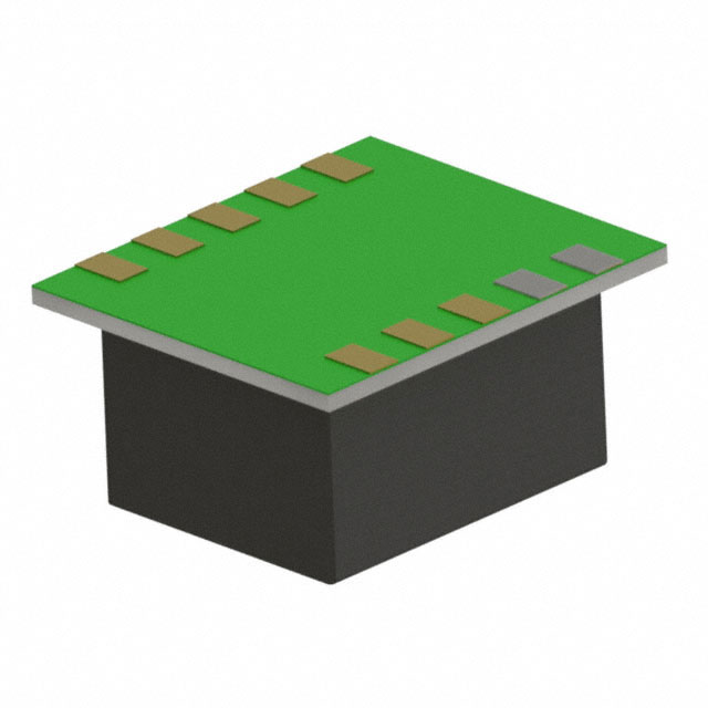
The MAXM15068 module is available in a low profile, compact 10-pin, 2.6mm × 3mm × 1.5mm, uSLIC™ package.
Applications
●● Industrial Sensors and Process Control
●● LDO Replacement
●● HVAC and Building Control
●● Battery-Powered Equipment
●● General Purpose Point-of-Load
●● High Efficiency
• Selectable PWM- or PFM-Mode of Operation
• Shutdown Current as Low as 2.2μA (typ)
●● Flexible Design
• Internal Soft-Start and Prebias Startup
• Open-Drain Power Good Output (RESET Pin)
• Programmable EN/UVLO Threshold
●● Robust Operation
• Hiccup Overcurrent Protection
• Overtemperature Protection
• -40°C to +125°C Ambient Operating Temperature/
-40°C to +150°C Junction Temperature
Ordering Information appears at end of data sheet.
uSLIC is a trademark of Maxim Integrated Products, Inc.
Typical Application Circuit
VIN
15.5V to 60V
CIN
R1
2.2MΩ
R2
191kΩ
VIN
OUT
RESET
GND
MAXM15068
C3
1µF
19-100645; Rev 0; 9/19
●● Easy to Use
• Wide 7.5V to 60V Input Range
• Adjustable 5V to 12V Output
• ±1.44% Feedback Accuracy
• Up to 200mA Output-Current
• Internally Compensated
• All Ceramic Capacitors
●● Rugged
• Complies with CISPR22 (EN55022) Class B
Conducted and Radiated Emissions
• Passes Drop, Shock, and Vibration Standards:
JESD22-B103, B104, B111
●● 4-20mA Current-Loop Powered Sensors
1µF
Benefits and Features
EN/UVLO
FB
VCC
LX
MODE
VOUT
12V, 200mA
COUT
4.7µF
R3
931kΩ
R4
75kΩ
�MAXM15068
Absolute Maximum Ratings
VIN, EN/UVLO to GND.............................................-0.3V to 70V
LX, OUT and GND......................................-0.3V to (VIN + 0.3V)
VCC, FB, RESET to GND...........................................-0.3V to 6V
MODE to GND........................................... -0.3V to (VCC + 0.3V)
Output Short-Circuit Duration.....................................Continuous
7.5V to 60V, 200mA Himalaya uSLIC
Step-Down Power Module
Junction Temperature (Note 1).........................................+150°C
Storage Temperature Range............................. -55°C to +125°C
Lead Temperature (soldering,10s)...................................+260°C
Soldering Temperature (reflow)........................................+260°C
Stresses beyond those listed under “Absolute Maximum Ratings” may cause permanent damage to the device. These are stress ratings only, and functional operation of the device at these
or any other conditions beyond those indicated in the operational sections of the specifications is not implied. Exposure to absolute maximum rating conditions for extended periods may affect
device reliability.
Package Information
PACKAGE TYPE: 10-PIN uSLIC
Package Code
M102A3+2
Outline Number
21-100094
Land Pattern Number
90-100027
THERMAL RESISTANCE, FOUR-LAYER BOARD (Note 2)
Junction-to-Ambient (θJA)
41.5°C/W
Note 1: Junction temperature greater than +125°C degrades operating lifetimes.
Note 2: Package thermal resistances are measured on an evaluation board with natural convection.
For the latest package outline information and land patterns (footprints), go to www.maximintegrated.com/packages. Note that a “+”,
“#”, or “-” in the package code indicates RoHS status only. Package drawings may show a different suffix character, but the drawing
pertains to the package regardless of RoHS status.
www.maximintegrated.com
Maxim Integrated │ 2
�MAXM15068
7.5V to 60V, 200mA Himalaya uSLIC
Step-Down Power Module
Electrical Characteristics
(VIN = VEN/UVLO = 24V, VGND = 0V, CVCC = 1μF, FB = 1V, LX = MODE = RESET = OUT = unconnected; TA = -40°C to +125°C, unless
otherwise noted. Typical values are at TA = +25°C. All voltages are referenced to GND, unless otherwise noted.) (Note 3)
PARAMETER
SYMBOL
CONDITIONS
MIN
TYP
MAX
UNITS
INPUT SUPPLY (VIN)
Input-Voltage Range
Input-Shutdown Current
Input-Supply Current
60
V
IIN-SH
VIN
VEN/UVLO = 0V, shutdown mode
7.5
2.2
4
μA
IQ-PFM
MODE = unconnected,
FB = 1.03 × VFB-REG
90
160
μA
IQ-PWM
Normal switching mode, MODE = 0
3.4
mA
ENABLE/UVLO (EN/UVLO)
EN/UVLO Threshold
EN/UVLO Input
leakage-Current
VENR
VEN/UVLO rising
1.19
1.215
1.28
VENF
VEN/UVLO falling
1.06
1.09
1.16
TA = +25° C
-100
7.5V < VIN < 60V, 0mA < IVCC < 10mA
4.75
IEN/UVLO
V
+100
nA
5
5.25
V
50
mA
LDO (VCC)
VCC Output-Voltage
Range
VCC Current Limit
VCC UVLO
VCC
IVCC-MAX
VCC = 4.3V
13
30
VCC-UVR
VCC rising
4.05
4.18
4.3
VCC-UVF
VCC falling
3.7
3.8
3.95
3.5
3.75
4
MODE = GND
0.887
0.9
0.913
MODE = unconnected
0.887
0.915
0.936
IFB
-100
-25
fSW
515
550
585
kHz
62.5
64.5
66.5
%
V
SOFT-START (SS)
Soft-Start Time
tSS
ms
FEEDBACK (FB)
FB-Regulation Voltage
FB-Leakage Current
VFB-REG
V
nA
TIMING
Switching Frequency
FB Undervoltage Trip
Level to Cause Hiccup
Hiccup Timeout
Minimum On-Time
Maximum Duty Cycle
www.maximintegrated.com
120
tON-MIN
DMAX
FB = 0.98 x FBREG
89
ms
90
120
ns
91.4
94
%
Maxim Integrated │ 3
�MAXM15068
7.5V to 60V, 200mA Himalaya uSLIC
Step-Down Power Module
Electrical Characteristics (continued)
(VIN = VEN/UVLO = 24V, VGND = 0V, CVCC = 1μF, FB = 1V, LX = MODE = RESET = OUT = unconnected; TA = -40°C to +125°C, unless
otherwise noted. Typical values are at TA = +25°C. All voltages are referenced to GND, unless otherwise noted.) (Note 3)
PARAMETER
RESET
SYMBOL
CONDITIONS
MIN
TYP
MAX
UNITS
FB Threshold for RESET
Rising
FB rising
93.5
95.5
97.5
%
FB Threshold for RESET
Falling
FB falling
90
92
94
%
RESET Delay After FB
Reaches 95% Regulation
1.9
ms
RESET Output Level
Low
IRESET = 5mA
0.2
V
RESET Output Leakage
Current
VRESET = 5.5V, TA = +25°C
0.1
μA
MODE
MODE Internal Pullup
Resistor
500
kΩ
166
°C
10
°C
THERMAL SHUTDOWN
Thermal-Shutdown
Threshold
Thermal-Shutdown
Hysteresis
Temperature rising
Note 3: Electrical specifications are production tested at TA = +25°C. Specifications over the entire operating temperature range are
guaranteed by design and characterization.
www.maximintegrated.com
Maxim Integrated │ 4
�MAXM15068
7.5V to 60V, 200mA Himalaya uSLIC
Step-Down Power Module
Typical Operating Characteristics
(VIN = VEN/UVLO = 24V, VGND = 0V, TA = -40°C to +125°C, unless otherwise noted. Typical values are at TA = +25°C. All voltages
are referenced to GND, unless otherwise noted. The circuit values for different output voltage applications are as in Table 1, unless
otherwise noted.)
EFFICIENCY vs. LOAD CURRENT
VOUT = 5V, PWM MODE
toc01
80
80
70
70
VIN = 7.5V
VIN = 12V
50
VIN = 24V
40
VIN = 36V
30
20
10
0
20
40
60
80
VIN = 15.5V
60
VIN = 24V
50
VIN = 36V
40
30
0
80 100 120 140 160 180 200
40
20
60 80 100 120 140 160 180 200
LOAD CURRENT (mA)
12.028
5.0380
12.026
50
40
VIN = 36V
30
VIN = 24V
20
1
5.0370
VIN = 7.5V
5.0365
VIN = 12V
5.0360
VIN = 24V
5.0355
VIN = 36V
5.0350
VIN = 15.5V
10
0
VIN = 60V
VIN = 48V
5.0340
100
toc07
12.28
12.022
VIN = 15.5V
12.020
VIN = 24V
12.018
VIN = 36V
VIN = 48V
80 100 120 140 160 180 200
12.012
VIN = 60V
0
20
40
60
80 100 120 140 160 180 200
LOAD CURRENT (mA)
OUTPUT VOLTAGE RIPPLE
VIN = 24V, VOUT = 5V
FULL LOAD, PWM MODE
toc08
toc09
VIN = 15.5V
12.24
5.100
VIN = 12V
VIN = 24V
VIN = 36V
5.088
5.076
5.064
VIN = 48V
VIN = 60V
5.052
5.040
OUTPUT VOLTAGE (V)
5.112
12.20
12.16
VIN = 24V
12.12
VIN = 36V
VIN = 48V
12.08
10mV/div
VOUT(AC)
VIN = 60V
12.04
12.00
5.028
5.016
60
OUTPUT VOLTAGE vs. LOAD CURRENT
VOUT = 12V, PFM MODE
VIN = 7.5V
5.124
40
12.024
LOAD CURRENT (mA)
OUTPUT VOLTAGE vs. LOAD CURRENT
VOUT = 5V, PFM MODE
5.136
20
100
toc06
12.014
VIN = 60V
0
10
LOAD CURRENT (mA)
12.016
VIN = 48V
5.0345
10
LOAD CURRENT (mA)
OUTPUT VOLTAGE (V)
5.0385
60
VIN = 7.5V
1
12.030
80
5.0375
VIN = 36V
OUTPUT VOLTAGE vs. LOAD CURRENT
VOUT = 12V, PWM MODE
toc05
5.0390
VIN = 48V
VIN = 24V
VIN = 12V
10
90
70
VIN = 60V
40
OUTPUT VOLTAGE vs. LOAD CURRENT
VOUT = 5V, PWM MODE
toc04
OUTPUT VOLTAGE (V)
EFFICIENCY (%)
50
0
0
EFFICIENCY vs. LOAD CURRENT
VOUT = 12V, PFM MODE
OUTPUT VOLTAGE (V)
60
20
VIN = 60V
LOAD CURRENT (mA)
100
70
30
VIN = 48V
10
VIN = 60V
0
90
20
VIN = 48V
toc03
100
EFFICIENCY (%)
90
60
toc02
100
90
EFFICIENCY (%)
EFFICIENCY (%)
100
EFFICIENCY vs. LOAD CURRENT
VOUT = 5V, PFM MODE
EFFICIENCY vs. LOAD CURRENT
VOUT = 12V, PWM MODE
0
20
40
60 80 100 120 140 160 180 200
LOAD CURRENT (mA)
www.maximintegrated.com
11.96
0
20
40
60
80 100 120 140 160 180 200
2µs/div
LOAD CURRENT (mA)
Maxim Integrated │ 5
�MAXM15068
7.5V to 60V, 200mA Himalaya uSLIC
Step-Down Power Module
Typical Operating Characteristics (continued)
(VIN = VEN/UVLO = 24V, VGND = 0V, TA = -40°C to +125°C, unless otherwise noted. Typical values are at TA = +25°C. All voltages
are referenced to GND, unless otherwise noted. The circuit values for different output voltage applications are as in Table 1, unless
otherwise noted.)
OUTPUT VOLTAGE RIPPLE
VIN = 24V, VOUT = 12V
FULL LOAD, PWM MODE
INTPUT VOLTAGE RIPPLE
VIN = 24V, VOUT = 5V
FULL LOAD, PWM MODE
toc10
10mV/div
VOUT(AC)
INTPUT VOLTAGE RIPPLE
VIN = 24V, VOUT = 12V
FULL LOAD, PWM MODE
toc11
VIN(AC)
50mV/div
LOAD TRANSIENT RESPONSE
VIN = 24V, VOUT = 5V, PFM MODE
LOAD STEP BETWEEN 5mA TO 50mA
2µs/div
LOAD TRANSIENT RESPONSE
VIN = 24V, VOUT = 5V, PWM MODE
LOAD STEP BETWEEN 100mA TO 200mA
toc13
50mV/div
VIN(AC)
2µs/div
2µs/div
toc12
LOAD TRANSIENT RESPONSE
VIN = 24V, VOUT = 12V, PFM MODE
LOAD STEP BETWEEN 5mA TO 50mA
toc14
toc15
200mV/div
100mV/div
VOUT(AC)
100mV/div
VOUT(AC)
VOUT(AC)
100mA/div
50mA/div
IOUT
IOUT
IOUT
100µs/div
100µs/div
100µs/div
STARTUP THROUGH ENABLE
VIN = 24V, VOUT = 5V
FULL LOAD, PWM MODE
LOAD TRANSIENT RESPONSE
VIN = 24V, VOUT = 12V, PWM MODE
LOAD STEP BETWEEN 100mA TO 200mA
50mA/div
SHUTDOWN THROUGH ENABLE
VIN = 24V, VOUT = 5V
FULL LOAD, PWM MODE
toc18
toc17
toc16
2V/div
VOUT(AC)
200mV/div
EN/UVLO
EN/UVLO
20V/div
2V/div
LX
100mA/div
VOUT
5V/div
RESET
IOUT
100µs/div
www.maximintegrated.com
1ms/div
2V/div
20V/div
LX
VOUT
2V/div
RESET
5V/div
100µs/div
Maxim Integrated │ 6
�MAXM15068
7.5V to 60V, 200mA Himalaya uSLIC
Step-Down Power Module
Typical Operating Characteristics (continued)
(VIN = VEN/UVLO = 24V, VGND = 0V, TA = -40°C to +125°C, unless otherwise noted. Typical values are at TA = +25°C. All voltages
are referenced to GND, unless otherwise noted. The circuit values for different output voltage applications are as in Table 1, unless
otherwise noted.)
STARTUP THROUGH ENABLE (2V PREBIAS)
VIN = 24V, VOUT = 5V
NO LOAD, PFM MODE
toc20
STARTUP THROUGH ENABLE (2V PREBIAS)
VIN = 24V, VOUT = 5V
NO LOAD, PWM MODE
toc19
2V/div
EN/UVLO
VOUT
5V/div
2V/div
EN/UVLO
EN/UVLO
20V/div
LX
VOUT
5V/div
1ms/div
SHUTDOWN THROUGH ENABLE
VIN = 24V, VOUT = 12V
FULL LOAD, PWM MODE
toc22
20V/div
LX
2V/div
RESET
RESET
toc21
2V/div
20V/div
2V/div
LX
STARTUP THROUGH ENABLE
VIN = 24V, VOUT = 12V
FULL LOAD, PWM MODE
5V/div
VOUT
5V/div
RESET
1ms/div
1ms/div
STARTUP THROUGH ENABLE (5V PREBIAS)
VIN = 24V, VOUT = 12V
NO LOAD, PWM MODE
toc23
STARTUP THROUGH ENABLE (5V PREBIAS)
VIN = 24V, VOUT = 12V
NO LOAD, PFM MODE
toc24
2V/div
EN/UVLO
2V/div
EN/UVLO
20V/div
LX
20V/div
LX
20V/div
LX
2V/div
EN/UVLO
5V/div
VOUT
5V/div
VOUT
RESET
5V/div
RESET
100µs/div
STARTUP THROUGH VIN
VIN = 24V, VOUT = 5V
FULL LOAD, PWM MODE
5V/div
5V/div
VOUT
1ms/div
SHUTDOWN THROUGH VIN
VIN = 24V, VOUT = 5V
FULL LOAD, PWM MODE
toc25
5V/div
RESET
1ms/div
STARTUP THROUGH VIN
VIN = 24V, VOUT = 12V
FULL LOAD, PWM MODE
toc26
20V/div
20V/div
VIN
20V/div
2V/div
LX
VIN
20V/div
VIN
LX
20V/div
LX
20V/div
2V/div
2V/div
5V/div
VCC
VCC
2V/div
VCC
VOUT
VOUT
2V/div
VOUT
1ms/div
www.maximintegrated.com
toc27
1ms/div
1ms/div
Maxim Integrated │ 7
�MAXM15068
7.5V to 60V, 200mA Himalaya uSLIC
Step-Down Power Module
Typical Operating Characteristics (continued)
(VIN = VEN/UVLO = 24V, VGND = 0V, TA = -40°C to +125°C, unless otherwise noted. Typical values are at TA = +25°C. All voltages
are referenced to GND, unless otherwise noted. The circuit values for different output voltage applications are as in Table 1, unless
otherwise noted.)
SHUTDOWN THROUGH VIN
VIN = 24V, VOUT = 12V
FULL LOAD, PWM MODE
OUTPUT SHORT IN STEADY STATE
VIN = 24V, VOUT = 5V
FULL LOAD, PWM MODE
toc29
toc28
OUTPUT SHORT DURING STARTUP
VIN = 24V, VOUT = 5V
FULL LOAD, PWM MODE
toc30
20V/div
5V/div
VIN
20V/div
LX
20V/div
SHORT
VIN
VOUT
VOUT
20V/div
LX
2V/div
VCC
5V/div
IOUT
5V/div
500mA/div
VOUT
OUTPUT SHORT IN STEADY STATE
VIN = 24V, VOUT = 12V
FULL LOAD, PWM MODE
10mA/div
20ms/div
OUTPUT SHORT DURING STARTUP
VIN = 24V, VOUT = 12V
FULL LOAD, PWM MODE
toc32
toc31
20V/div
5V/div
SHORT
VIN
VOUT
10V/div
VOUT
LX
20V/div
LX
IOUT
500mA/div
20ms/div
www.maximintegrated.com
20V/div
LX
IOUT
20ms/div
1ms/div
20mV/div
20mV/div
20V/div
IOUT
10mA/div
20ms/div
Maxim Integrated │ 8
�MAXM15068
7.5V to 60V, 200mA Himalaya uSLIC
Step-Down Power Module
Typical Operating Characteristics (continued)
(VIN = VEN/UVLO = 24V, VGND = 0V, TA = -40°C to +125°C, unless otherwise noted. Typical values are at TA = +25°C. All voltages
are referenced to GND, unless otherwise noted. The circuit values for different output voltage applications are as in Table 1, unless
otherwise noted.)
100
100
OUTPUT CURRENT vs. AMBIENT TEMPERATURE
toc34
60
60
40
40
40
40
20
20
20
20
0
0
GAIN
-20
-40
CROSSOVER FREQUENCY = 25.642kHz
PHASE MARGIN = 53.439°
-60
-80
-20
1k
10k
FREQUENCY (Hz)
GAIN (dB)
80
60
PHASE MARGIN (◦)
80
PHASE
PHASE
0
-40
-40
-60
-60
-80
100k
-80
80
0
GAIN
-20
-20
CROSSOVER FREQUENCY = 18.440kHz
PHASE MARGIN = 53.679 °
1k
-40
200
150
VOUT = 12V
100
VOUT = 5V
50
-60
-80
100k
10k
toc35
250
100
60
80
GAIN (dB)
toc33
OUTPUT CURRENT (mA)
100
BODE PLOT
VIN = 24V, VOUT = 12V
FULL LOAD, PWM MODE
PHASE MARGIN (◦)
BODE PLOT
VIN = 24V, VOUT = 5V
FULL LOAD, PWM MODE
0
50
FREQUENCY (Hz)
70
90
110
130
AMBIENT TEMPERATURE (°C)
RADIATED EMISSION PLOT
LEMI_1 = SHORT, CEMI_1 = CEMI_2 = OPEN
toc37
50
CISPR-22 CLASS B QP LIMIT
MAGNITUDE (dBµV/m)
40
30
VERTICAL
SCAN
20
10
HORIZONTAL
SCAN
0
-10
30M
1G
100M
FREQUENCY(Hz)
CONDITIONS : VIN = 24V, VOUT = 12V, IOUT = 0.2A
FROM MAXM15068EVKIT#
www.maximintegrated.com
Maxim Integrated │ 9
�MAXM15068
7.5V to 60V, 200mA Himalaya uSLIC
Step-Down Power Module
Pin Configuration
TOP VIEW
+
10
VIN
9
VIN
8
EN/UVLO
4
7
VCC
5
6
FB
LX
1
GND
2
RESET
3
MODE
OUT
MAXM15068
‘+’ INDICATES PIN 1 OF THE MODULE
10-PIN
(2.6mm × 3mm × 1.5mm)
Pin Description
PIN
NAME
1
LX
2
GND
3
RESET
Open-Drain Power Good Output. Pull up RESET to an external power supply with an external resistor.
RESET goes low if FB drops below 92% of its set value. RESET goes high impedance 1.9ms after FB
rises above 95.5% of its set value. See the Electrical Characteristics table for threshold values.
4
MODE
PFM/PWM Mode-Selection Input. Connect MODE to GND to enable fixed-frequency PWM operation at all
loads. Leave MODE unconnected for PFM operation at light load.
5
OUT
Module Output Pin. Connect a capacitor from OUT to GND. See PCB Layout Guidelines section for more
details.
6
FB
Output Feedback Connection. Connect FB to a resistor-divider between OUT and GND to set the output
voltage.
7
VCC
8
EN/UVLO
9,10
VIN
www.maximintegrated.com
FUNCTION
Switching Node of the Inductor. No external connection to this pin.
Ground Pin. Connect GND to the ground plane. See the PCB Layout Guidelines section for more details.
Refer to the MAXM15068 EV kit for a sample layout.
Internal LDO Power Output. Bypass VCC to GND with a minimum 1µF ceramic capacitor.
Active-High, Enable/Undervoltage-Detection Input. Pull EN/UVLO to GND to disable the module output.
Connect EN/UVLO to VIN for always-on operation. Connect a resistor-divider between VIN, EN/UVLO, and
GND to program the input voltage at which the module turns on.
Power-Supply Input. Connect the VIN pins together. Decouple to GND with a capacitor;
place the capacitor close to the VIN and GND pins. See Table 1 for more details.
Maxim Integrated │ 10
�MAXM15068
7.5V to 60V, 200mA Himalaya uSLIC
Step-Down Power Module
Functional Diagram
Internal Diagram
MAXM15068
VCC
VIN
LDO
HIGH-SIDE
DRIVER
LX
+
EN/UVLO
68µH
1.215V
OUT
OSCILLATOR
PEAK
CURRENT-MODE
CONTROLLER
LOW-SIDE
DRIVER
SOFT-START
MODE
FB
www.maximintegrated.com
MODE
SELECTION
LOGIC
GND
SLOPE
COMPENSATION
RESET
LOGIC
RESET
Maxim Integrated │ 11
�MAXM15068
Detailed Description
The MAXM15068 module is a high-voltage, synchronous
step-down DC-DC module with integrated MOSFETs and
inductor, that operates over a wide 7.5V to 60V input
voltage range. The module delivers output current up to
200mA over a programmable output-voltage range of 5V
to 12V. When EN/UVLO and VCC UVLO are ascertained,
an internal power-up sequence ramps up the error-amplifier reference, resulting in an output-voltage soft-start.
The FB pin monitors the output voltage through a resistordivider. The RESET pin transitions to a high-impedance
state 1.9ms after the output voltage reaches 95.5% of
regulation. The device selects either PFM or forcedPWM mode depending on the state of the MODE pin at
power-up. By pulling the EN/UVLO pin to low, the device
enters shutdown mode and consumes only 2.2μA (typ) of
standby current.
The module uses an internally compensated, fixed-fre
quency, current-mode control scheme. On the rising edge
of an internal clock, the high-side pMOSFET turns on.
An internal error amplifier compares the feedback voltage to a fixed internal reference voltage and generates
an error voltage. The error voltage is compared to a sum
of the current-sense voltage and a slope-compensation
voltage by a PWM comparator to set the on-time. During
the on-time of the pMOSFET, the inductor current ramps
up. For the remainder of the switching period (off-time),
the pMOSFET is kept off and the low-side nMOSFET
turns on. During the off-time, the inductor releases the
stored energy as the inductor current ramps down, providing current to the output. Under overload conditions,
the cycle-by-cycle current-limit feature limits the inductor
peak current by turning off the high-side pMOSFET and
turning on the low-side nMOSFET.
Mode Selection (MODE)
The logic state of the MODE pin is latched after VCC
and EN/UVLO voltages exceed respective UVLO rising
thresholds and all internal voltages are ready to allow
LX switching. If the MODE pin is unconnected at powerup, the part operates in PFM mode at light loads. If the
MODE pin is grounded at power-up, the part operates in
constant-frequency PWM mode at all loads. State changes on the MODE pin are ignored during normal operation.
PWM Mode
In PWM mode, the module output current is allowed to
go negative. PWM mode is useful in frequency sensitive applications and provides fixed switching frequency
operation at all loads.
www.maximintegrated.com
7.5V to 60V, 200mA Himalaya uSLIC
Step-Down Power Module
PFM Mode
PFM mode disables negative output current from the module, and skips pulses at light loads for better efficiency. In
PFM mode, the module output current is forced to a fixed
peak of 60mA in every clock cycle until the output voltage
rises to 102.3% of the nominal value. Once the output
voltage reaches 102.3% of the nominal value, the highside switch is turned off and the low-side switch is turned
on. Once the module output current hits zero cross, LX
goes to a high-impedance state and the module enters
hibernate operation until the load current discharges the
output voltage to 101.1% of the nominal value. Most of
the internal blocks are turned off in hibernate operation
to save quiescent current. When the output voltage falls
below 101.1% of the nominal value, the module comes
out of hibernate operation, turns on all internal blocks, and
commences the process of delivering pulses of energy
until the output voltage reaches 102.3% of the nominal
value. The module naturally comes out of PFM mode
and serves load requirements when the module output
demands more than 60mA peak. At light loads, PFM
mode gives higher efficiency compared to PWM mode
because of lower quiescent current drawn from supply.
Internal 5V Regulator
An internal regulator provides a 5V nominal supply to
power the internal functions and to drive the power
MOSFETs. The output of the linear regulator (VCC)
should be bypassed with a 1μF ceramic capacitor to
GND. An undervoltage lockout circuit disables the buck
converter when VCC falls below 3.8V (typ). The 400mV,
VCC-UVLO hysteresis prevents chattering on power-up
and power-down.
Enable/Undervoltage Lockout (EN/UVLO),
Soft-Start
When EN/UVLO voltage is above 1.215V (typ), the
device’s internal error-amplifier reference voltage starts
to ramp up. The duration of the soft-start ramp is 3.75ms
(typ), allowing a smooth increase of the output voltage.
Driving EN/UVLO low disables both power MOSFETs, as
well as other internal circuitry, and reduces VIN quiescent
current to below 2.2μA. EN/UVLO can be used as an
input-voltage UVLO adjustment input. An external voltage-divider between VIN and EN/UVLO to GND adjusts
the input voltage at which the device turns on or turns off.
If input UVLO programming is not desired, connect EN/
UVLO to VIN (see the Electrical Characteristics table for
EN/UVLO rising and falling threshold voltages).
Maxim Integrated │ 12
�MAXM15068
7.5V to 60V, 200mA Himalaya uSLIC
Step-Down Power Module
RESET Output (RESET)
where:
The device includes an open-drain RESET output to
monitor the output voltage. RESET goes high impedance
1.9ms after the output rises above 95.5% of its nominal
set value and pulls low when the output voltage falls
below 92% of the set nominal regulated voltage. RESET
asserts low during the hiccup timeout period.
Startup into a Prebiased Output
The device is capable of soft-start into a prebiased output, without discharging the output capacitor in both the
PFM and forced-PWM modes. Such a feature is useful in
applications where digital integrated circuits with multiple
rails are powered.
Overcurrent Protection (OCP)/Hiccup Mode
The device is provided with a robust overcurrent protection (OCP) scheme that protects the device under overload and output short-circuit conditions. When overcurrent
is detected or if the FB node goes below 64.5% of its
nominal regulation threshold, the device enters hiccup
mode of operation. In hiccup mode, the device is protected by suspending switching for a hiccup timeout period
of 120ms (typ). Once the hiccup timeout period expires,
soft-start is attempted again. Hiccup mode of operation
ensures low power dissipation under output short-circuit
conditions. The device exits hiccup mode if the overcurrent condition is removed or if VIN or EN/UVLO is cycled.
Thermal Overload Protection
Thermal overload protection limits the total power
dissipation in the device. When the junction temperature
exceeds +166°C, an on-chip thermal sensor shuts down
the device, turns off the internal power MOSFETs, allowing the device to cool down. The thermal sensor turns the
device on after the junction temperature cools by 10°C.
VOUT = Steady-state output voltage,
IOUT = Maximum load current,
fSW = Worst-case switching frequency (585 kHz),
DMAX = Maximum duty cycle (0.89),
tON(MIN) = Worst-case minimum controllable switch ontime (120ns).
Selection of Input Capacitor
The input filter capacitor reduces peak currents drawn
from the power source and reduces noise and voltage
ripple on the input caused by the converter’s switching.
The input capacitor RMS current requirement (IRMS) is
defined by the following equation:
IRMS = IOUT(MAX) ×
IRMS(MAX) =
+ 0.4
IOUT(MAX)
2
Choose an input capacitor that exhibits less than +10°C
temperature rise at the RMS input current for optimal
long-term reliability. Use low-ESR ceramic capacitors with
high-ripple-current capability at the input. X7R capacitors
are recommended in industrial applications for their temperature stability. Calculate the input capacitance using
the following equation:
Applications Information
The minimum and maximum operating input voltages for
a given output voltage should be calculated as follows:
VIN
where IOUT(MAX) is the maximum load current. IRMS has
a maximum value when the input voltage equals twice the
output voltage (VIN = 2 × VOUT). So,
CIN =
Input Voltage Range
√VOUT × (VIN − VOUT)
IOUT MAX × DMAX × (1 − DMAX)
(
)
fSW × ∆ VIN
where:
DMAX = Maximum duty cycle (0.89),
fSW = Switching frequency,
∆VIN = Allowable input-voltage ripple.
VOUT
VIN(MAX) = t
ON(MIN) × fSW
www.maximintegrated.com
Maxim Integrated │ 13
�MAXM15068
7.5V to 60V, 200mA Himalaya uSLIC
Step-Down Power Module
Selection of Output Capacitor
Small ceramic X7R-grade capacitors are sufficient and
recommended for output-voltage generation. The output
capacitor has two functions. It provides smooth voltage,
stores sufficient energy to support the output voltage
under load transient conditions, and stabilizes the device’s
internal control loop. Usually the output capacitor is sized
to support a step load of 50% of the maximum output current in the application, such that the output-voltage deviation is less than 3%. Required output capacitance can be
calculated from the following equation:
30
COUT = V
OUT
where COUT is the output capacitance in μF and VOUT
is the output voltage. Derating of ceramic capacitors with
DC-voltage must be considered while selecting the output
capacitor.
Setting the Input Undervoltage-Lockout Level
The device offers an adjustable input undervoltage lockout level. Set the voltage at which the device turns on with
a resistive voltage-divider connected from VIN to GND
(see Figure 1). Connect the center node of the divider to
EN/UVLO.
Choose R1 to be 2.2MΩ (max), and then calculate R2 as
follows:
R2 =
R1 × 1.215
(VINU − 1.215)
where VINU is the voltage at which the device is required
to turn on.
If the EN/UVLO pin is driven from an external signal
source, a series resistance of minimum 1kΩ is recommended to be placed between the signal source output
and the EN/UVLO pin to reduce voltage ringing on the
line.
Output Voltage Setting
The MAXM15068 typical output voltage can be programmed from 5V to 12V. Set the output voltage by connecting a resistor-divider from output to FB to GND (see
Figure 2).
Choose R4 to be less than or equal to 75kΩ and calculate
R3 with the following equation:
R3 = R4 ×
(
VOUT
−1
)
OUT
VIN
MAXM15068
R1
0.9
R3
MAXM15068
FB
EN/UVLO
R4
R2
Figure 1. Adjustable EN/UVLO Network
Figure 2. Setting the Output Voltage
Table 1. Selection of Components
V IN(MIN)
(V)
V IN(MAX)
(V)
V OUT
(V)
7.5
60
5
15.5
60
12
www.maximintegrated.com
C OUT
R3
(kΩ)
R4
(kΩ)
1 x 1µF 1206 100V
(TAIYO YUDEN HMK316B7105KLH)
1 x 10µF 0805 16V
(MURATA GRM21BZ71C106KE15)
348
75
1 x 1µF 1206 100V
(TAIYO YUDEN HMK316B7105KLH)
1 x 4.7µF 0805 25V
(MURATA GRM21BZ71E475KE15)
931
75
C IN
Maxim Integrated │ 14
�MAXM15068
7.5V to 60V, 200mA Himalaya uSLIC
Step-Down Power Module
Power Dissipation
To operate in high ambient temperature, the device output
current needs to be derated. See the Typical Operating
Characteristics section for the derating curves to use as
a guide.
PCB Layout Guidelines
●● Keep the output capacitors as close as possible to
the OUT and GND pins.
●● Keep the resistive feedback dividers as close as
possible to the FB pin.
●● Keep the power traces and load connections short.
Refer to EV kit layout for first-pass success.
Use the following guidelines for good PCB layout:
●● Keep the input capacitors as close as possible to the
VIN and GND pins.
VIN
VOUT
OUT
VIN
CIN
COUT
MAXM15068
R1
R3
RESET
R2
EN/UVLO
FB
VCC
LX
CVCC
R4
MODE
GND
CIN
GND PLANE
1
GND
2
+
LX
MAXM15068
VIN PLANE
10
VIN
9
VIN
R1
RESET
3
8
EN/UVLO
MODE
4
7
VCC
OUT
5
6
R2
CVCC
FB
VOUT PLANE
COUT
R3
GND PLANE
R4
VIA TO INNER LAYER FOR ROUTING FB
Figure 3. Layout Guidelines
www.maximintegrated.com
Maxim Integrated │ 15
�MAXM15068
7.5V to 60V, 200mA Himalaya uSLIC
Step-Down Power Module
Typical Application Circuits
Typical Application Circuit for 12V Output
VIN
15.5V to 60V
C1
1µF
R1
2.2MΩ
VIN
OUT
RESET
GND
VOUT
12V, 200mA
C2
4.7µF
R3
931kΩ
MAXM15068
R2
191kΩ
C3
EN/UVLO
FB
VCC
LX
R4
75kΩ
MODE
1µF
MODE = GND FOR PWM
MODE = OPEN FOR PFM
C1 = TAIYO YUDEN 1μF/X7R/100V/1206 (HMK316B7105KLH)
C2 = MURATA 4.7μF/X7R/25V/0805 (GRM21BZ71E475KE15)
C3 = TAIYO YUDEN 1μF/X7R/16V/0603 (EMK107B7105KA)
Typical Application Circuit for 5V Output
VIN
7.5V to 60V
C1
1µF
R1
2.2MΩ
VIN
OUT
RESET
GND
VOUT
5V, 200mA
C2
10µF
R3
348kΩ
MAXM15068
R2
442kΩ
C3
EN/UVLO
FB
VCC
LX
1µF
MODE
R4
75kΩ
MODE = GND FOR PWM
MODE = OPEN FOR PFM
C1 = TAIYO YUDEN 1μF/X7R/100V/1206 (HMK316B7105KLH)
C2 = MURATA 10μF/X7R/16V/0805 (GRM21BZ71C106KE15)
C3 = TAIYO YUDEN 1μF/X7R/16V/0603 (EMK107B7105KA)
www.maximintegrated.com
Maxim Integrated │ 16
�MAXM15068
7.5V to 60V, 200mA Himalaya uSLIC
Step-Down Power Module
Ordering Information
PART NUMBER
TEMP RANGE
PIN-PACKAGE
MAXM15068AMB+
-40°C
to +125°C
10-pin uSLIC
MAXM15068AMB+T
-40°C to +125°C
10-pin uSLIC
+Denotes a lead(Pb)-free/RoHS-compliant package.
T = Tape and reel.
www.maximintegrated.com
Maxim Integrated │ 17
�MAXM15068
7.5V to 60V, 200mA Himalaya uSLIC
Step-Down Power Module
Revision History
REVISION
NUMBER
REVISION
DATE
0
9/19
DESCRIPTION
Initial release
PAGES
CHANGED
—
For pricing, delivery, and ordering information, please visit Maxim Integrated’s online storefront at https://www.maximintegrated.com/en/storefront/storefront.html.
Maxim Integrated cannot assume responsibility for use of any circuitry other than circuitry entirely embodied in a Maxim Integrated product. No circuit patent licenses
are implied. Maxim Integrated reserves the right to change the circuitry and specifications without notice at any time. The parametric values (min and max limits)
shown in the Electrical Characteristics table are guaranteed. Other parametric values quoted in this data sheet are provided for guidance.
Maxim Integrated and the Maxim Integrated logo are trademarks of Maxim Integrated Products, Inc.
© 2019 Maxim Integrated Products, Inc. │ 18
�


 工商网监
湘ICP备2023018690号
工商网监
湘ICP备2023018690号
