Click here for production status of specific part numbers.
MAXM17546
4.5V to 42V, 5A High-Efficiency, DC-DC Step-Down
Power Module with Integrated Inductor
General Description
Benefits and Features
The device operates over a wide input voltage range
of 4.5V to 42V and delivers up to 5A continuous output
current with excellent line and load regulation over an
output-voltage range of 0.9V to 12V. The high level of
integration significantly reduces design complexity, manufacturing risks, and offers a true plug-and-play power
supply solution, reducing time-to-market.
●● Saves Board Space in Space-Constrained
Applications
• Complete Integrated Step-Down Power Supply in a
Single Package
• Small Profile 9mm x 15mm x 4.32mm SiP Package
• Simplified PCB Design with Minimal External BOM
Components
The Himalaya series of voltage regulator ICs and power
modules enable cooler, smaller and simpler power supply
solutions. The MAXM17546 is an easy-to-use, step-down
power module that combines a switching power supply
controller, dual n-channel MOSFET power switches, fully
shielded inductor, and the compensation components in
a low-profile, thermally-efficient system-in-package (SiP).
The device can be operated in the pulse-width modulation
(PWM), pulse-frequency modulation (PFM), or discontinuous conduction mode (DCM) control schemes.
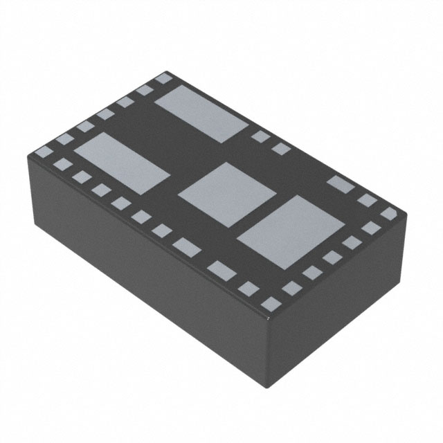
The MAXM17546 is available in a low-profile, highly
thermal-emissive, compact, 29-pin, 9mm x 15mm x
4.32mm SiP package that reduces power dissipation in
the package and enhances efficiency. The package is
easily soldered onto a printed circuit board and suitable
for automated circuit board assembly.
Applications
●●
●●
●●
●●
●●
Test and Measurement Equipment
Distributed Supply Regulation
FPGA and DSP Point-of-Load Regulator
Base-Station Point-of-Load Regulator
HVAC and Building Control
●● Reduces Design Complexity, Manufacturing Risks,
and Time-to-Market
• Integrated Synchronous Step-Down DC-DC
Converter
• Integrated Inductor
• Integrated FETs
• Integrated Compensation Components
●● Offers Flexibility for Power-Design Optimization
• Wide Input-Voltage Range from 4.5V to 42V
• Output-Voltage Adjustable Range from 0.9V to 12V
• Adjustable Frequency with External Frequency
Synchronization (100kHz to 2.2MHz)
• PWM, PFM, or DCM Current-Mode Control
• Programmable Soft-Start
• Auxiliary Bootstrap LDO for Improved Efficiency
• Optional Programmable EN/UVLO
●● Operates Reliably in Adverse Industrial Environments
• Integrated Thermal Protection
• Hiccup Mode Overload Protection
• RESET Output-Voltage Monitoring
• Ambient Operating Temperature Range
(-40°C to +125°C) / Junction Temperature Range
(-40°C to +150°C)
Ordering Information appears at end of data sheet.
19-100146; Rev 0; 4/18
�MAXM17546
4.5V to 42V, 5A High-Efficiency, DC-DC Step-Down
Power Module with Integrated Inductor
Typical Application Circuit
VIN
7.5V TO 42V
CIN
2 x10µF
IN
EN/UVLO
R3
665kΩ
VCC
R1
191kΩ
MAXM17546 EXTVCC
FB
DL
BST
RESET
LX
SS
CF
MODE/SYNC
CSS
22nF
VOUT
OUT
SGND
PGND
CF
2.2pF
COUT
3 x 22µF
R2
42.2kΩ
RT
CIN: 10µF GRM32ER71H106KA12
COUT: 22µF GRM32ER71C226MEA8
www.maximintegrated.com
Maxim Integrated │ 2
�MAXM17546
4.5V to 42V, 5A High-Efficiency, DC-DC Step-Down
Power Module with Integrated Inductor
Absolute Maximum Ratings
IN to PGND............................................................-0.3V to +48V
EN/UVLO, SS to SGND.........................................-0.3V to +48V
LX to PGND................................................-0.3V to (VIN + 0.3V)
BST to PGND.........................................................-0.3V to +53V
BST to LX..............................................................-0.3V to +6.5V
BST to VCC............................................................-0.3V to +48V
FB, CF, RESET, MODE/SYNC, RT to SGND.......-0.3V to +6.5V
DL, VCC to PGND.................................................-0.3V to +6.5V
SGND to PGND.....................................................-0.3V to +0.3V
EXTVCC to PGND.................................................-0.3V to +26V
OUT to PGND (VIN ≤16V)...........................-0.3V to (VIN + 0.3V)
OUT to PGND (VIN > 16V).......................................-0.3V to 16V
Output Short-Circuit Duration.....................................Continuous
Operating Temperature Range ............................-40°C to 125°C
Junction Temperature (Note 1).........................................+150°C
Storage Temperature Range................................-55°C to 150°C
Soldering Temperature (reflow)........................................+240°C
Stresses beyond those listed under “Absolute Maximum Ratings” may cause permanent damage to the device. These are stress ratings only, and functional operation of the device at these
or any other conditions beyond those indicated in the operational sections of the specifications is not implied. Exposure to absolute maximum rating conditions for extended periods may affect
device reliability.
Package Information
PACKAGE TYPE: 29-PIN SiP
Package Code
L29915#1
Outline Number
21-100177
Land Pattern Number
90-100055
THERMAL RESISTANCE, FOUR-LAYER BOARD (Note 2)
Junction to Ambient (θJA)
24ºC/W
For the latest package outline information and land patterns (footprints), go to www.maximintegrated.com/packages. Note that a “+”,
“#”, or “-” in the package code indicates RoHS status only. Package drawings may show a different suffix character, but the drawing
pertains to the package regardless of RoHS status.
Note 1: Junction temperature greater than +125°C degrades operating lifetimes.
Note 2: Package thermal resistance is measured on an evaluation board with natural convection.
Electrical Characteristics
(VIN = VEN/UVLO = 24V, RRT = OPEN (450kHz), VPGND = VSGND = VMODE/SYNC = 0V, LX = SS = RESET = CF = DL = VCC = OUT
= open, VEXTVCC = 0V, VBST to VLX = 5V, VFB = 1V, TA = -40°C to +125°C, unless otherwise noted. Typical values are at TA = +25°C.
All voltages are referenced to SGND, unless otherwise noted.) (Note 3)
PARAMETER
SYMBOL
CONDITIONS
MIN
TYP
MAX
UNITS
42
V
16
μA
INPUT SUPPLY (VIN)
Input-Voltage Range
Input-Shutdown Current
Input-Quiescent Current
VIN
4.5
IIN_SH
VEN/UVLO = 0V, (Shutdown mode)
IQ_PFM
MODE/SYNC = open
128
11
IQ_DCM
DCM Mode
1.27
IQ_PWM
PWM Mode, no load,
VOUT = VEXTVCC = 5V
μA
2
mA
18
ENABLE/UNDERVOLTAGE LOCKOUT (EN/UVLO)
EN/UVLO Threshold
Enable Pullup Resistor
www.maximintegrated.com
VENR
VEN/UVLO rising
1.185
1.215
1.245
VENF
VEN/UVLO falling
1.06
1.09
1.12
RENP
Pullup resistor between IN and
EN/UVLO pins
3.15
3.32
3.45
V
MΩ
Maxim Integrated │ 3
�MAXM17546
4.5V to 42V, 5A High-Efficiency, DC-DC Step-Down
Power Module with Integrated Inductor
Electrical Characteristics (continued)
(VIN = VEN/UVLO = 24V, RRT = OPEN (450kHz), VPGND = VSGND = VMODE/SYNC = 0V, LX = SS = RESET = CF = DL = VCC = OUT
= open, VEXTVCC = 0V, VBST to VLX = 5V, VFB = 1V, TA = -40°C to +125°C, unless otherwise noted. Typical values are at TA = +25°C.
All voltages are referenced to SGND, unless otherwise noted.) (Note 3)
PARAMETER
SYMBOL
CONDITIONS
MIN
TYP
MAX
UNITS
6V < VIN < 42V, IVCC = 1mA
4.75
5
5.25
1mA < IVCC < 45mA
4.75
5
5.25
VCC = 4.3V, VIN = 7V
50
90
150
mA
0.4
V
LOW DROPOUT (INLDO)
VCC Output-Voltage
Range
VCC Current Limit
IN to VCC Dropout
VCC UVLO
VCC
IVCC_MAX
VCC_DO
VIN = 4.5V, IVCC = 45mA
VCC_UVR
VCC rising
4.1
4.2
4.3
VCC_UVF
VCC falling
3.7
3.8
3.9
V
V
LOW DROPOUT (EXTVCC)
EXTVCC OperatingVoltage Range
4.84
EXTVCC Switch-Over
Voltage
24
Rising
4.56
4.7
4.84
Falling
4.33
4.45
4.6
EXTVCC to VCC Dropout
VEXTVCC_DO
VEXTVCC = 5V, IEXTVCC = 45mA
EXTVCC Current Limit
IEXTVCC_MAX VCC = 4.3V, EXTVCC = 8V
V
V
0.6
V
45
85
140
mA
4.7
5
5.3
μA
SOFT-START (SS)
Charging Current
ISS
VSS = 0.5V
OUTPUT SPECIFICATIONS
Line-Regulation Accuracy
VIN = 6.5V to 42V, VOUT = 5V
Load-Regulation Accuracy
Tested with IOUT = 0A to 5A at VOUT = 5V
FB-Regulation Voltage
VFB_REG
FB Input-Bias Current
IFB
FB Undervoltage Trip Level
to Cause Hiccup
0.1
mV/V
6
mV/A
MODE/SYNC = SGND or MODE = VCC
0.8875
0.9
0.9135
MODE/SYNC = OPEN
0.8875
0.915
0.936
0 < VFB < 1V
VFB_HICF
-75
0.55
HICCUP Timeout
0.58
V
+75
nA
0.61
V
32768
Cycles
MODE/SYNC PIN
MODE Threshold
VM_DCM
MODE/SYNC = VCC (DCM Mode)
VM_PFM
MODE/SYNC = OPEN (PFM mode)
VM_PWM
MODE/SYNC = GND (PWM mode)
SYNC FrequencyCapture Range
fSW set by RRT
SYNC Pulse Width
SYNC Threshold
www.maximintegrated.com
VCC - 0.6
V
VCC / 2
0.6
1.1 x
fSW
1.4 x
fSW
50
VIH
VIL
kHz
ns
2.0
0.8
V
Maxim Integrated │ 4
�MAXM17546
4.5V to 42V, 5A High-Efficiency, DC-DC Step-Down
Power Module with Integrated Inductor
Electrical Characteristics (continued)
(VIN = VEN/UVLO = 24V, RRT = OPEN (450kHz), VPGND = VSGND = VMODE/SYNC = 0V, LX = SS = RESET = CF = DL = VCC = OUT
= open, VEXTVCC = 0V, VBST to VLX = 5V, VFB = 1V, TA = -40°C to +125°C, unless otherwise noted. Typical values are at TA = +25°C.
All voltages are referenced to SGND, unless otherwise noted.) (Note 3)
PARAMETER
SYMBOL
CONDITIONS
MIN
TYP
MAX
UNITS
CURRENT LIMIT
Average Current-Limit
Threshold
IAVG_LIMIT
6.75
A
RT PIN
Switching Frequency
fSW
Minimum On-Time
tON(MIN)
Minimum Off-time
tOFF(MIN)
LX Dead Time
RESET PIN
RRT = 196KΩ
90
100
110
RRT = open
420
450
480
RRT = 7.5kΩ
1950
2200
2450
114
160
ns
160
ns
140
tDT
22
RESET Output-Level Low
IRESET = 10mA
RESET Output-Leakage
Current
VRESET = 5.5V
-100
kHz
ns
400
mV
100
nA
VOUT Threshold for
RESET Assertion
VOUT_OKF
VFB falling
90.4
92.5
94.6
%
VOUT Threshold for
RESET Deassertion
VOUT_OKR
VFB rising
93.4
95.5
97.7
%
RESET Deassertion Delay
after FB Reaches 95%
Regulation
1024
Cycles
165
°C
10
°C
THERMAL SHUTDOWN
Thermal-Shutdown
Threshold
Thermal-Shutdown
Hystersis
Temperature Rising
Note 3: Electrical specifications are production tested at TA = + 25°C. Specifications over the entire operating temperature range are
guaranteed by design and characterization.
www.maximintegrated.com
Maxim Integrated │ 5
�MAXM17546
4.5V to 42V, 5A High-Efficiency, DC-DC Step-Down
Power Module with Integrated Inductor
Typical Operating Characteristics
(VIN = VEN/UVLO = 24V, VSGND = VPGND = 0V, TA = -40°C to +125°C, unless otherwise noted. Typical values are at TA = +25°C.
All voltages are referenced to GND, unless otherwise noted. The circuit values for different output-voltage applications are as in
Table 1, unless otherwise noted.)
EFFICIENCY vs. LOAD CURRENT
(3.3V OUTPUT, PWM MODE, fSW = 400kHz)
toc01
100
toc02
90
80
80
70
70
60
VIN = 36V
40
VIN = 24V
30
VIN = 12V
20
10
0
1000
2000
3000
4000
60
VIN = 12V
50
40
VIN = 24V
20
10
10
5000
0
1000
toc04
80
70
70
EFFICIENCY (%)
3000
4000
5000
VIN = 36V
VIN = 12V
VIN = 24V
toc05
60
50
VIN = 36V
40
30
40
20
1
10
100
1000
LOAD CURRENT (mA)
EFFICIENCY vs. LOAD CURRENT
(0.9V OUTPUT, PWM MODE, fSW = 300kHz)
EFFICIENCY vs. LOAD CURRENT
(1.2V OUTPUT, PWM MODE, fSW = 400kHz)
toc08
100
100
90
80
80
80
70
70
70
EFFICIENCY (%)
90
30
10
0
1000
50
VIN = 12V
30
VIN = 5V
20
60
40
2000
3000
4000
LOAD CURRENT (mA)
www.maximintegrated.com
5000
10
0
1000
1
10
100
1000
EFFICIENCY vs. LOAD CURRENT
(1.5V OUTPUT, PWM MODE, fSW = 400kHz)
toc09
60
50
VIN = 12V
40
30
VIN = 5V
20
VIN = 12V
LOAD CURRENT (mA)
90
VIN = 12V
VIN = 24V
30
VIN = 24V
LOAD CURRENT (mA)
50
VIN = 36V
50
0
60
toc06
60
10
toc07
1000
70
0
1000
100
80
10
40
10
90
VIN = 12V
10
100
1
100
20
10
VIN = 12V
EFFICIENCY vs. LOAD CURRENT
(5V OUTPUT, DCM MODE, fSW = 450kHz)
EFFICIENCY vs. LOAD CURRENT
(3.3V OUTPUT, DCM MODE, fSW = 400kHz)
20
1
VIN = 24V
LOAD CURRENT (mA)
EFFICIENCY (%)
EFFICIENCY (%)
90
80
100
EFFICIENCY (%)
100
90
30
2000
VIN = 36V
40
LOAD CURRENT (mA)
100
40
50
30
EFFICIENCY vs. LOAD CURRENT
(5V OUTPUT, PFM MODE, fSW = 450kHz)
50
60
20
LOAD CURRENT (mA)
60
70
30
EFFICIENCY (%)
50
EFFICIENCY (%)
90
80
VIN = 36V
toc03
100
90
EFFICIENCY (%)
EFFICIENCY (%)
100
EFFICIENCY vs. LOAD CURRENT
(3.3V OUTPUT, PFM MODE, fSW = 400kHz)
EFFICIENCY vs. LOAD CURRENT
(5V OUTPUT, PWM MODE, fSW = 450kHz)
VIN = 5V
20
2000
3000
4000
LOAD CURRENT (mA)
5000
10
0
1000
2000
3000
4000
5000
LOAD CURRENT (mA)
Maxim Integrated │ 6
�MAXM17546
4.5V to 42V, 5A High-Efficiency, DC-DC Step-Down
Power Module with Integrated Inductor
Typical Operating Characteristics (continued)
(VIN = VEN/UVLO = 24V, VSGND = VPGND = 0V, TA = -40°C to +125°C, unless otherwise noted. Typical values are at TA = +25°C.
All voltages are referenced to GND, unless otherwise noted. The circuit values for different output-voltage applications are as in
Table 1, unless otherwise noted.)
EFFICIENCY vs. LOAD CURRENT
(1.8V OUTPUT, PWM MODE, fSW = 400kHz)
toc10
100
90
90
80
80
80
VIN = 12V
50
40
VIN = 5V
60
VIN = 12V
50
40
30
VIN = 24V
20
10
70
2000
1000
3000
4000
10
5000
70
EFFICIENCY (%)
VIN = 36V
50
40
VIN = 24V
2000
3000
5000
4000
80
80
70
40
5000
VIN = 12V
VIN = 5V
50
500
40
5000
toc17
80
80
EFFICIENCY (%)
80
VIN = 5V
60
VIN = 12V
70
500
LOAD CURRENT (mA)
www.maximintegrated.com
VIN = 12V
VIN = 24V
50
40
50
VIN = 5V
60
5000
50
500
LOAD CURRENT (mA)
500
5000
toc18
70
VIN = 5V
VIN = 12V
60
VIN = 24V
50
40
5
50
100
90
5
5
EFFICIENCY vs. LOAD CURRENT
(2.5V OUTPUT, PFM MODE, fSW = 400kHz)
90
40
VIN = 12V
LOAD CURRENT (mA)
90
50
VIN = 5V
60
EFFICIENCY vs. LOAD CURRENT
(1.8V OUTPUT, PFM MODE, fSW = 400kHz)
100
5000
70
LOAD CURRENT (mA)
toc16
4000
toc15
50
5
3000
100
90
60
2000
1000
EFFICIENCY vs. LOAD CURRENT
(1.2V OUTPUT, PFM MODE, fSW = 400kHz)
90
EFFICIENCY vs. LOAD CURRENT
(1.5V OUTPUT, PFM MODE, fSW = 400kHz)
70
0
LOAD CURRENT (mA)
toc14
LOAD CURRENT (mA)
100
4000
50
20
1000
3000
EFFICIENCY (%)
EFFICIENCY (%)
80
0
VIN = 24V
20
100
90
10
40
EFFICIENCY vs. LOAD CURRENT
(0.9V OUTPUT, PFM MODE, fSW = 300kHz)
toc13
30
2000
VIN = 12V
50
LOAD CURRENT (mA)
EFFICIENCY vs. LOAD CURRENT
(12V OUTPUT, PWM MODE, fSW = 900kHz)
60
1000
VIN = 36V
60
10
0
LOAD CURRENT (mA)
100
70
30
VIN = 24V
20
0
EFFICIENCY (%)
VIN = 5V
60
EFFICIENCY (%)
70
toc12
100
90
30
EFFICIENCY (%)
EFFICIENCY vs. LOAD CURRENT
(8V OUTPUT, PWM MODE, fSW = 800kHz)
toc11
100
EFFICIENCY (%)
EFFICIENCY (%)
EFFICIENCY vs. LOAD CURRENT
(2.5V OUTPUT, PWM MODE, fSW = 400kHz)
5000
5
50
500
5000
LOAD CURRENT (mA)
Maxim Integrated │ 7
�MAXM17546
4.5V to 42V, 5A High-Efficiency, DC-DC Step-Down
Power Module with Integrated Inductor
Typical Operating Characteristics (continued)
(VIN = VEN/UVLO = 24V, VSGND = VPGND = 0V, TA = -40°C to +125°C, unless otherwise noted. Typical values are at TA = +25°C.
All voltages are referenced to GND, unless otherwise noted. The circuit values for different output-voltage applications are as in
Table 1, unless otherwise noted.)
EFFICIENCY vs. LOAD CURRENT
(12V OUTPUT, PFM MODE, fSW = 900kHz)
EFFICIENCY vs. LOAD CURRENT
(8V OUTPUT, PFM MODE, fSW = 800kHz)
toc19
90
90
80
80
70
VIN = 36V
VIN = 12V
60
VIN = 24V
50
40
5
50
500
toc20
100
EFFICIENCY (%)
EFFICIENCY (%)
100
70
VIN = 36V
60
VIN = 24V
50
5000
40
5
50
500
5000
LOAD CURRENT (mA)
LOAD CURRENT (mA)
STEADY-STATE SWITCHING WAVEFORMS
(VIN = 24V, VOUT = 5V, IOUT = 5A
PWM MODE, MODE = SGND)
STEADY-STATE SWITCHING WAVEFORMS
(VIN = 24V, VOUT = 5V, IOUT = 0A
PWM MODE, MODE = SGND)
toc22
toc21
VOUT
20mV/div
(ACCOUPLED)
VOUT
20mV/div
(ACCOUPLED)
VLX
10V/div
VLX
10V/div
2µs/div
2µs/div
STEADY-STATE SWITCHING WAVEFORMS
(VIN = 24V, VOUT = 5V, IOUT = 100mA
DCM MODE, MODE = VCC)
STEADY-STATE SWITCHING WAVEFORMS
(VIN = 24V, VOUT = 5V, IOUT = 25mA
PFM MODE, MODE = OPEN)
toc24
toc23
VOUT
100mV/div
(ACCOUPLED)
VOUT
10mV/div
(ACCOUPLED)
VLX
10V/div
VLX
10V/div
100µs/div
www.maximintegrated.com
1µs/div
Maxim Integrated │ 8
�MAXM17546
4.5V to 42V, 5A High-Efficiency, DC-DC Step-Down
Power Module with Integrated Inductor
Typical Operating Characteristics (continued)
(VIN = VEN/UVLO = 24V, VSGND = VPGND = 0V, TA = -40°C to +125°C, unless otherwise noted. Typical values are at TA = +25°C.
All voltages are referenced to GND, unless otherwise noted. The circuit values for different output-voltage applications are as in
Table 1, unless otherwise noted.)
OUTPUT VOLTAGE vs. LOAD CURRENT
(5V OUTPUT, PWM MODE, fSW = 450kHz)
OUTPUT VOLTAGE vs. LOAD CURRENT
(5V OUTPUT, PFM MODE, fSW = 450kHz)
toc25
5.02
5.15
OUTPUT VOLTAGE (V)
OUTPUT VOLTAGE (V)
5.00
4.98
4.96
VIN = 24V
4.94
VIN = 12V
VIN = 42V
4.92
4.90
toc26
5.20
5
50
5.10
5.05
5.00
4.95
VIN = 12V
4.90
4.85
500
4.80
5000
5
50
toc27
toc28
3.45
3.32
3.40
3.30
OUTPUT VOLTAGE (V)
OUTPUT VOLTAGE (V)
5000
OUTPUT VOLTAGE vs. LOAD CURRENT
(3.3V OUTPUT, PFM MODE, fSW = 400kHz)
OUTPUT VOLTAGE vs. LOAD CURRENT
(3.3V OUTPUT, PWM MODE, fSW = 400kHz)
3.28
3.26
VIN = 24V
3.24
VIN = 42V
VIN = 12V
3.35
3.30
VIN = 24V
3.25
3.22
3.20
500
LOAD CURRENT (mA)
LOAD CURRENT (mA)
3.34
VIN = 42V
VIN = 24V
VIN = 12V
VIN = 42V
5
50
500
5000
3.20
5
50
500
5000
LOAD CURRENT (mA)
LOAD CURRENT (mA)
POWER-UP AND DOWN THROUGH EN/UVLO
(VIN = 24V, VOUT = 5V, IOUT = 25mA
PFM MODE, MODE = OPEN)
POWER-UP AND DOWN THROUGH EN/UVLO
(VIN = 24V, VOUT = 3.3V, IOUT = 25mA
PFM MODE, MODE = OPEN)
toc29
toc30
2V/div
VEN/UVLO
VOUT
5V/div
VRESET
5V/div
4ms/div
www.maximintegrated.com
2V/div
VEN/UVLO
VOUT
2V/div
VRESET
5V/div
4ms/div
Maxim Integrated │ 9
�MAXM17546
4.5V to 42V, 5A High-Efficiency, DC-DC Step-Down
Power Module with Integrated Inductor
Typical Operating Characteristics (continued)
(VIN = VEN/UVLO = 24V, VSGND = VPGND = 0V, TA = -40°C to +125°C, unless otherwise noted. Typical values are at TA = +25°C.
All voltages are referenced to GND, unless otherwise noted. The circuit values for different output-voltage applications are as in
Table 1, unless otherwise noted.)
POWER-UP AND DOWN THROUGH EN/UVLO
(VIN = 24V, VOUT = 5V, IOUT = 5A
PWM MODE, MODE = SGND)
POWER-UP AND DOWN THROUGH EN/UVLO
(VIN = 24V, VOUT = 3.3V, IOUT = 5A
PWM MODE, MODE = SGND)
toc32
toc31
2V/div
VEN/UVLO
VEN/UVLO
2V/div
VOUT
5V/div
VOUT
2V/div
VRESET
5V/div
VRESET
5V/div
IOUT
5A/div
IOUT
5A/div
4ms/div
4ms/div
POWER-UP WITH 2.5V BIAS
(VIN = 24V, VOUT = 5V, IOUT = 0A
PWM MODE, MODE = SGND)
POWER-UP WITH 2.5V BIAS
(VIN = 24V, VOUT = 3.3V, IOUT = 0A
PWM MODE, MODE = SGND)
toc34
toc33
2V/div
VEN/UVLO
2V/div
VEN/UVLO
2V/div
VOUT
1V/div
VOUT
5V/div
VRESET
5V/div
VRESET
4ms/div
4ms/div
LOAD TRANSIENT
(VIN = 24V, VOUT = 5V, IOUT = 0A TO 2.5A
PWM MODE, MODE = SGND)
LOAD TRANSIENT
(VIN = 24V, VOUT = 3.3V, IOUT = 0A TO 2.5A
PWM MODE, MODE = SGND)
toc36
toc35
100mV/div
(ACCOUPLED)
VOUT
VOUT
100mV/div
(ACCOUPLED)
IOUT
1A/div
1A/div
IOUT
200µs/div
www.maximintegrated.com
400µs/div
Maxim Integrated │ 10
�MAXM17546
4.5V to 42V, 5A High-Efficiency, DC-DC Step-Down
Power Module with Integrated Inductor
Typical Operating Characteristics (continued)
(VIN = VEN/UVLO = 24V, VSGND = VPGND = 0V, TA = -40°C to +125°C, unless otherwise noted. Typical values are at TA = +25°C.
All voltages are referenced to GND, unless otherwise noted. The circuit values for different output-voltage applications are as in
Table 1, unless otherwise noted.)
LOAD TRANSIENT
(VIN = 24V, VOUT = 5V, IOUT = 2.5A TO 5A
PWM MODE, MODE = SGND)
LOAD TRANSIENT
(VIN = 24V, VOUT = 3.3V, IOUT = 2.5A TO 5A
PWM MODE, MODE = SGND)
toc38
toc37
VOUT
100mV/div
(ACCOUPLED)
VOUT
100mV/div
(ACCOUPLED)
IOUT
2A/div
IOUT
2A/div
400µs/div
400µs/div
LOAD TRANSIENT
(VIN = 24V, VOUT = 5V, IOUT = 25mA TO 2.5A
PFM MODE, MODE = OPEN)
toc39
LOAD TRANSIENT
(VIN = 24V, VOUT = 3.3V, IOUT = 25mA TO 2.5A
PFM MODE, MODE = OPEN)
toc40
VOUT
100mV/div
(ACCOUPLED)
VOUT
100mV/div
(ACCOUPLED)
IOUT
1A/div
IOUT
1A/div
1ms/div
400µs/div
LOAD TRANSIENT
(VIN = 24V, VOUT = 5V, IOUT = 25mA TO 2.5A
DCM MODE, MODE = VCC)
toc41
IOUT
VOUT
100mV/div
(ACCOUPLED)
IOUT
1A/div
1A/div
400µs/div
www.maximintegrated.com
toc42
100mV/div
(ACCOUPLED)
VOUT
LOAD TRANSIENT
(VIN = 24V, VOUT = 3.3V, IOUT = 25mA TO 2.5A
DCM MODE, MODE = VCC)
400µs/div
Maxim Integrated │ 11
�MAXM17546
4.5V to 42V, 5A High-Efficiency, DC-DC Step-Down
Power Module with Integrated Inductor
Typical Operating Characteristics (continued)
(VIN = VEN/UVLO = 24V, VSGND = VPGND = 0V, TA = -40°C to +125°C, unless otherwise noted. Typical values are at TA = +25°C.
All voltages are referenced to GND, unless otherwise noted. The circuit values for different output-voltage applications are as in
Table 1, unless otherwise noted.)
STARTUP INTO SHORT
(VIN = 24V, VOUT = 5V, OUTPUT SHORT
PWM MODE, MODE = SGND)
OUTPUT SHORT IN STEADY STATE
(VIN = 24V, VOUT = 5V, OUTPUT SHORT
PWM MODE, MODE = SGND)
toc44
toc43
500mV/div
VOUT
2V/div
VEN/UVLO
VOUT
VLX
20V/div
IOUT
5A/div
500mV/div
VLX
20V/div
IOUT
5A/div
2ms/div
20ms/div
SYNC FREQUENCY AT 630kHz
(VIN = 24V, VOUT = 5V, IOUT = 5A
PWM MODE, MODE = SGND)
BODE PLOT
(VIN = 24V, VOUT = 5V, IOUT = 5A)
toc46
40
PHASE
30
100
80
20
2V/div
VLX
60
10
GAIN (dB)
VSYNC
40
0
-40
0
-20
fCR = 36kHz,
PHASE MARGIN = 62°
-30
2µs/div
20
GAIN
-10
-20
10V/div
120
103
PHASE (°)
toc45
-40
105
104
-60
FREQUENCY (Hz)
BODE PLOT
(VIN = 24V, VOUT = 3.3V, IOUT = 5A)
toc47
40
PHASE
30
20
GAIN
-10
-20
0
-20
fCR = 39kHz,
PHASE MARGIN = 63°
-30
103
www.maximintegrated.com
104
FREQUENCY (Hz)
-40
105
-60
OUTPUT CURRENT (A)
0
PHASE (°)
60
40
toc48
5
80
10
GAIN (dB)
6
100
20
-40
120
OUTPUT CURRENT
vs. AMBIENT TEMPERATURE
4
3
VOUT = 5V
2
VOUT = 3.3V
1
0
0
20
40
60
80
100
120
AMBIENT TEMPERATURE (°C)
Maxim Integrated │ 12
�MAXM17546
4.5V to 42V, 5A High-Efficiency, DC-DC Step-Down
Power Module with Integrated Inductor
Pin Configuration
MODE/SYNC
IN
PGND
DL
OUT
26
25
OUT
+
VCC
29
1
28
27
23
OUT
22
OUT
21
PGND
20
PGND
19
PGND
18
PGND
17
PGND
24
RESET
2
RT
3
SGND
4
CF
5
MAXM17546
EP1
EP2
EP3
FB
6
7
8
SS
EN/UVLO
9
IN
10
11
PGND
EXTVCC
12
BST
13
LX
14
15
PGND
PGND
16
PGND
9mm x 15mm x 4.32mm 29-PIN SiP
Pin Description
PIN
NAME
FUNCTION
1
VCC
5V LDO Output. The VCC is bypassed to PGND internally through a 2.2µF capacitor. Do not connect any external components to the VCC pin.
2
RESET
3
RT
4
SGND
5
CF
Compensation Pin. Connect a 2.2pF capacitor from CF to FB.
6
FB
Feedback Input. Connect FB to the center tap of an external resistor-divider from the OUT to
SGND to set the output voltage.
7
SS
Soft-Start Input. Connect a capacitor from SS to SGND to set the soft-start time.
8
EN/UVLO
www.maximintegrated.com
Open-Drain RESET Output. The RESET output is driven low if FB drops below 92% of its set
value. RESET goes high 1024 clock cycles after FB rises above 95% of its set value.
Switching Frequency Programming Pin. Connect a resistor from RT to SGND to set the
regulator's switching frequency. Leave RT open for the default 450kHz frequency.
Analog Ground.
Enable/Undervoltage-Lockout Input. Connect a resistor from EN/UVLO to SGND to set the UVLO
threshold. By default, the module is enabled with the EN/UVLO pin open.
Maxim Integrated │ 13
�MAXM17546
4.5V to 42V, 5A High-Efficiency, DC-DC Step-Down
Power Module with Integrated Inductor
Pin Description (continued)
PIN
NAME
9, 28
IN
10,
14-21, 27
PGND
11
EXTVCC
12
BST
13
LX
22-25
OUT
26
DL
FUNCTION
Power-Supply Input. Decouple to PGND with a capacitor; place the capacitor close to the
IN and PGND pins.
Power Ground
External Power Supply Input for the Internal LDO. Applying a voltage between 4.7V and 24V at
the EXTVCC pin bypasses the internal LDO and improves efficiency.
Boost Flying Capacitor Node. Internally a 0.1μF is connected from BST to LX. Do not connect any
external components to the BST pin.
Switching Node. Leave unconnected; do not connect any external components to the LX pin.
Regulator Output Pin. Connect a capacitor from OUT to PGND.
Gate Drive for Low-Side MOSFET. Do not connect any external components to the DL pin.
29
MODE/SYNC
MODE Pin Configures the Part to Operate in PWM, PFM, or DCM Modes of Operation.
Leave MODE unconnected for PFM operation (pulse skipping at light loads). Connect MODE
to SGND for constant frequency PWM operation at all loads. Connect MODE to VCC for DCM
operation. The device can be synchronized to an external clock using this pin.
See the MODE/SYNC setting section for more details.
EP1, EP2,
EP3
—
Exposed Pad. Create a large copper plane below the module connecting EP1, EP2, and
EP3 to improve heat dissipation capability. PGND and SGND are shorted through this plane.
www.maximintegrated.com
Maxim Integrated │ 14
�MAXM17546
4.5V to 42V, 5A High-Efficiency, DC-DC Step-Down
Power Module with Integrated Inductor
Functional Diagrams
Internal Diagram
MAXM17546
VCC
IN
LDO
SELECT
1µF
1µF
2.2µF
EXTVCC
INLDO
4.7Ω
0.1µF
BST
3.32MΩ
LDO
0.1µF
CURRENT- SENSE
LOGIC
SGND
LX
PEAK
CURRENTMODE
CONTROLLER
EN/UVLO
1.215V
4.7µH
OUT
0.22µF
HICCUP
RT
4.7Ω
OSCILLATOR
PGND
DL
CF
FB
MODE-SELECTION
LOGIC
ERROR AMPLIFIER/
LOOP COMPENSATION
VCC
MODE/
SYNC
SLOPE
COMPENSATION
SWITCHOVER
LOGIC
RESET
5μA
SS
HICCUP
FB
RESET
LOGIC
EN/UVLO
www.maximintegrated.com
Maxim Integrated │ 15
�MAXM17546
4.5V to 42V, 5A High-Efficiency, DC-DC Step-Down
Power Module with Integrated Inductor
Detailed Description
The MAXM17546 is a high-efficiency, high-voltage,
synchronous step-down module with dual-integrated
MOSFETs that operates over a 4.5V to 42V input, and
supports a programmable output voltage from 0.9V to
12V, delivering up to 5A current. Built-in compensation
for the entire output-voltage range eliminates the need
for external components. The feedback (FB) regulation
accuracy over -40°C to +125°C is ±1.5%.
The device features a peak-current-mode control architecture. An internal transconductance-error amplifier produces an integrated error voltage at an internal node that
sets the duty cycle using a PWM comparator, a highside current-sense amplifier, and a slope-compensation
generator. At each rising edge of the clock, the high-side
MOSFET turns on and remains on until either the appropriate or maximum duty cycle is reached, or the peak
current limit is detected. During the high-side MOSFET’s
on-time, the inductor current ramps up. During the second
half of the switching cycle, the high-side MOSFET turns
off and the low-side MOSFET turns on. The inductor
releases the stored energy as its current ramps down
and provides current to the output. The device features
a MODE/SYNC pin that can be used to operate the
device in PWM, PFM, or DCM control schemes and to
synchronize the switching frequency to an external clock.
The device integrates adjustable-input undervoltage lockout, adjustable soft-start, open-drain RESET, auxiliary
bootstrap LDO, and DL-to-LX short-detection features.
Mode Selection (MODE)
The logic state of the MODE/SYNC pin is latched when
VCC and EN/UVLO voltages exceed the respective UVLO
rising thresholds and all internal voltages are ready to
allow LX switching. If the MODE/SYNC pin is open at
power-up, the device operates in PFM mode at light
loads. If the MODE/SYNC pin is grounded at power-up,
the device operates in constant-frequency PWM mode
at all loads. Finally, if the MODE/SYNC pin is connected
to VCC at power-up, the device operates in constant
frequency DCM mode at light loads. State changes on the
MODE/SYNC pin are ignored during normal operation.
PWM-Mode Operation
In PWM mode, the inductor current is allowed to go
negative. PWM operation provides constant frequency
operation at all loads, and is useful in applications
sensitive to changes in switching frequency. However,
the PWM mode of operation gives lower efficiency at light
loads compared to PFM and DCM modes of operation.
www.maximintegrated.com
PFM-Mode Operation
The PFM mode of operation disables negative inductor
current and additionally skips pulses at light loads for high
efficiency. In PFM mode, the inductor current is forced to
a fixed peak of 2A (typ) every clock cycle until the output
rises to 102.3% of the nominal voltage. Once the output
reaches 102.3% of the nominal voltage, both the highside and low-side FETs are turned off and the device
enters hibernate operation until the load discharges the
output to 101.1% of the nominal voltage. Most of the
internal blocks are turned off in hibernate operation to
minimize quiescent current. After the output falls below
101.1% of the nominal voltage, the device comes out
of hibernate operation, turns on all internal blocks, and
again commences the process of delivering pulses of
energy to the output until it reaches 102.3% of the nominal output voltage. The advantage of the PFM mode is
higher efficiency at light loads because of lower quiescent
current drawn from the supply. The disadvantage is that
the output-voltage ripple is higher compared to PWM or
DCM modes of operation and switching frequency is not
constant at light loads.
DCM-Mode Operation
DCM mode of operation features constant frequency
operation down to lighter loads than PFM mode, by not
skipping pulses but only disabling negative inductor
current at light loads. DCM operation offers efficiency
performance that lies between PWM and PFM modes
Linear Regulator
The MAXM17546 has two internal low-dropout (LDO)
regulators that powers VCC. During power-up, when the
EN/UVLO pin voltage is above the true shutdown voltage, then the VCC is powered from INLDO. When VCC
voltage is above the VCC UVLO threshold and EXTVCC
voltage is greater than 4.7V (typ) the VCC is powered from
EXTVCC LDO. Only one of the two LDOs is in operation at a time depending on the voltage level present at
EXTVCC. Powering VCC from EXTVCC increases efficiency at higher input voltages. EXTVCC voltage should
not exceed 24V.
Typical VCC output voltage is 5V. Internally VCC is
bypassed with a 2.2μF ceramic capacitor to PGND.
See the Electrical Characteristics table for the current limit details for both the regulators. In applications
where the buck converter output is connected to the
EXTVCC pin, if the output is shorted to ground, then
the transfer from EXTVCC LDO to INLDO happens
seamlessly without any impact on the normal functionality.
Maxim Integrated │ 16
�MAXM17546
4.5V to 42V, 5A High-Efficiency, DC-DC Step-Down
Power Module with Integrated Inductor
Setting the Switching Frequency (RT)
The switching frequency of the MAXM17546 can be
programmed from 100kHz to 2.2MHz by using a resistor
connected from RT to SGND. The switching frequency
(fSW) is related to the resistor connected at the RT pin
(RRT) by the following equation:
R RT ≅
19 × 10 3
− 1.7
f SW
of PFM/DCM. When the external clock is removed on-fly
then the internal oscillator frequency changes to the RT
set frequency and the converter still continues to operate
in PWM mode. The minimum external clock pulse-width
high should be greater than 50ns. See the MODE/SYNC
section in the Electrical Characteristics table for details.
DL-to-OUT Short Detection
where RRT is in kΩ and fSW is in kHz. Leaving the RT pin
open causes the device to operate at the default switching
frequency of 450kHz. See the Electrical Characteristics
table for RT resistor value recommendations for a few
common frequencies.
In MAXM17546, DL and OUT pins are adjacent to each
other. To prevent damage to the low-side FET in case
the DL pin is shorted to the OUT pins, the DL-to-OUT
short detection feature has been implemented. If the
MAXM17546 detects that the DL pin is shorted to the OUT
pins before startup, the startup sequence is not initiated
and output voltage is not soft-started.
Operating Input-Voltage Range
Overcurrent-Protection/HICCUP Mode
The minimum and maximum operating input voltages for
a given output voltage should be calculated as follows:
VIN( MIN ) ≅
(
)+ I
( OUTMAX × 0.075)
1 − (f SW ( MAX ) × t OFF ( MAX) )
VOUT + I OUT ( MAX ) × 0.038
VIN( MAX) =
VOUT
f SW ( MAX ) × t ON( MIN)
where VOUT is the steady-state output voltage, IOUT(MAX)
is the maximum load current, fSW(MAX) is the maximum
switching frequency, tOFF(MAX) is the worst-case minimum switch off-time (160ns), and tON(MIN) is the worstcase minimum switch on-time (160ns).
The Component Selection Table, Table 1 provides the
operating input-voltage range and the optimum switchingfrequency range for the different selected output voltages.
External Frequency Synchronization
The internal oscillator of the MAXM17546 can be synchronized to an external clock signal on the MODE/SYNC
pin. The external synchronization clock frequency must
be between 1.1 x fSW and 1.4 x fSW, where fSW is the frequency programmed by the RT resistor. When an external
clock is applied to the MODE/SYNC pin, the internal oscillator frequency changes to the external clock frequency
(from the original frequency based on the RT setting) after
detecting 16 external clock edges. The converter operates
in PWM mode during synchronization operation. When
the external clock is applied to the MODE/SYNC pin, the
mode of operation changes to PWM from the initial state
www.maximintegrated.com
The MAXM17546 is provided with a robust overcurrent
protection scheme that protects the device under overload
and output short-circuit conditions. If output voltage drops
to 68% (typ) of its nominal value any time after soft-start
is complete, hiccup mode is triggered. In addition, one
occurrence of peak inductor current exceeding the 8.8A
(typ) level triggers a hiccup mode. In hiccup mode, the
converter is protected by suspending switching for a hiccup timeout period of 32768 clock cycles. Once the hiccup
timeout period expires, soft-start is attempted again.
RESET Output
The MAXM17546 includes a comparator to monitor the
output voltage. The open-drain RESET output requires an
external pullup resistor. RESET goes high (high impedance) 1024 switching cycles after the regulator output
increases above 95.5% of the designed nominal regulated voltage. RESET goes low when the regulator output
voltage drops to below 92.5% of the nominal regulated
voltage. RESET also goes low during thermal shutdown.
Prebiased Output
When the MAXM17546 starts into a prebiased output,
both the high-side and the low-side switches are turned
off so that the converter does not sink current from the
output. High-side and low-side switches do not start
switching until the PWM comparator commands the first
PWM pulse, at which point switching commences. The
output voltage is then smoothly ramped up to the target
value in alignment with the internal reference.
Maxim Integrated │ 17
�MAXM17546
4.5V to 42V, 5A High-Efficiency, DC-DC Step-Down
Power Module with Integrated Inductor
Thermal-Shutdown Protection
Thermal shutdown protection limits total power dissipation in the MAXM17546. When the junction temperature
of the device exceeds +165°C (typ), an on-chip thermal
sensor shuts down the device, allowing the device to cool.
The thermal sensor turns the device on again after the
junction temperature cools by 10°C. Soft-start resets
during thermal shutdown. Carefully evaluate the total
power dissipation (see the Power Dissipation section)
to avoid unwanted triggering of the thermal shutdown in
normal operation.
Output-Capacitor Selection
X7R ceramic output capacitors are preferred due to their
stability over temperature in industrial applications. The
output capacitors are usually sized to support a step load
of 50% of the maximum output current in the application,
so the output-voltage deviation is contained to 3% of the
output-voltage change. The minimum required output
capacitance can be calculated as follows:
C OUT=
0.33
1
+
t RESPONSE ≅
f SW
fC
Applications Information
Input-Capacitor Selection
1 I STEP × t RESPONSE
×
∆VOUT
2
The input-filter capacitor reduces peak currents drawn
from the power source and reduces noise and voltage
ripple on the input caused by the circuit’s switching.
The input capacitor RMS current requirement (IRMS) is
defined by the following equation:
where:
VOUT × (VIN − VOUT )
=
IRMS I OUT ( MAX) ×
VIN
fC = Target closed-loop crossover frequency,
where, IOUT(MAX) is the maximum load current. IRMS has
a maximum value when the input voltage equals twice
the output voltage (VIN = 2 x VOUT), so IRMS(MAX) =
IOUT(MAX)/2. Choose an input capacitor that exhibits less
than a +10°C temperature rise at the RMS input current
for optimal long-term reliability. Use low-ESR ceramic
capacitors with high ripple-current capability at the input.
X7R capacitors are recommended in industrial applications for their temperature stability. The CIN capacitor
values in Table 1 are the minimum recommended values
for the associated operating conditions.
In applications where the source is located distant from
the MAXM17546 input, an electrolytic capacitor should
be added in parallel to the ceramic capacitor to provide
necessary damping for potential oscillations caused by
the inductance of the longer input power path and input
ceramic capacitor.
www.maximintegrated.com
ISTEP = Load-current step,
tRESPONSE = Response time of the controller,
VOUT = Allowable output-voltage deviation,
fSW = Switching frequency.Select fC to be 1/10th of fSW if
the swtiching frequency is less than or equal to 400kHz.
Select fC to be 40kHz if the switching frequency is more
than 400kHz.
Soft-Start Capacitor Selection
The MAXM17546 implements adjustable soft-start operation to reduce inrush current. A capacitor connected
from the SS pin to SGND programs the soft-start time.
The selected output capacitance (CSEL) and the output
voltage (VOUT) determine the minimum required soft-start
capacitor as follows:
C SS ≥ 28 × 10 −6 × C SEL × VOUT
The soft-start time (tSS) is related to the capacitor
connected at SS (CSS) by the following equation:
t SS =
C SS
5.55
where tSS is in milliseconds and CSS is in nanofarads.
For example, to program a 4ms soft-start time, a 22nF
capacitor should be connected from the SS pin to SGND.
Maxim Integrated │ 18
�MAXM17546
4.5V to 42V, 5A High-Efficiency, DC-DC Step-Down
Power Module with Integrated Inductor
Setting the Input Undervoltage-Lockout Level
The MAXM17546 offers an adjustable input undervoltage
lockout level. Set the voltage at which MAXM17546 turns
on. Calculate R3 as follows:
R3 =
3.32 × 1.215
(VINU − 1.215)
Adjusting Output Voltage
Set the output voltage with a resistive voltage-divider
connected from the positive terminal of the output capacitor (VOUT) to SGND (see Figure 2). Connect the center
node of the divider to the FB pin. To choose the resistive
voltage-divider values calculate for resistor R1, then R2.
where R3 is in MΩ and VINU is the voltage at which the
MAXM17546 is required to turn on. Ensure that VINU is
higher than 0.8 x VOUT.
First, calculate resistor R1 from the output to FB as
follows:
451× 10 3
R1 =
f C × C OUT
Loop Compensation
where:
The MAXM17546 is internally loop-compensated. Connect
a 2.2pF capacitor from CF to FB for stable operation.
R1 is in kΩ
Typically, designs with crossover frequency (fC) less than
fSW/10 and less than 40kHz offers good phase margin
and transient response. For other choices of fC, the
design should be carefully evaluated according to user
requirements.
COUT = Derated value of the capacitor due to DC bias (µF)
fC = Desired crossover frequency (kHz)
Then, calculate resistor R2 from FB to SGND as follows:
R2 =
R1× 0.9
− 0.9)
(VOUT
VOUT
MAXM17546
IN
R1
MAXM17546
FB
EN/UVLO
R3
R2
SGND
SGND
Figure 1. Setting the Input-Undervoltage Lockout
Figure 2. Setting the Output Voltage
Component Selection Table
Table 1. Selection Component Values
V IN (V)
V OUT (V)
C IN
C OUT
R1 (kΩ)
R2 (kΩ)
fSW (kHz)
R RT (kΩ)
4.5 to 16
0.9
2 x 10μF, 1210, X7R, 50V
12 x 47μF, 1210, X7R, 6.3V
33.2
Open
300
61.9
4.5 to 17
1.2
2 x 10μF, 1210, X7R, 50V
9 x 47μF, 1210, X7R, 6.3V
39.2
118
400
45.3
4.5 to 21
1.5
2 x 10μF, 1210, X7R, 50V
7 x 47μF, 1210, X7R, 6.3V
52.3
78.7
400
45.3
4.5 to 26
1.8
2 x 10μF, 1210, X7R, 50V
5 x 47μF, 1210, X7R, 6.3V
71.5
71.5
400
45.3
4.5 to 35
2.5
2 x 10μF, 1210, X7R, 50V
4 x 47μF, 1210, X7R, 6.3V
71.5
40.2
400
45.3
4.5 to 42
3.3
2 x 10μF, 1210, X7R, 100V
3 x 47μF, 1210, X7R, 10V
158
59
400
45.3
7.5 to 42
5
2 x 10μF, 1210, X7R, 100V
3 x 22μF, 1210, X7R, 10V
191
42.2
450
Open
10 to 42
8
2 x 10μF, 1210, X7R, 100V
3 x 22μF, 1210, X7R, 16V
232
29.4
800
22.1
18 to 42
12
2 x 10μF, 1210, X7R, 100V
2 x 22μF, 1210, X7R, 16V
340
27.4
900
19.6
www.maximintegrated.com
Maxim Integrated │ 19
�MAXM17546
4.5V to 42V, 5A High-Efficiency, DC-DC Step-Down
Power Module with Integrated Inductor
Power Dissipation
Ensure that the junction temperature of the MAXM17546
does not exceed +125°C under the operating conditions
specified for the power supply. At a given operating condition, the power losses that lead to temperature rise of the
part are estimated as follows:
POUT 2
1
= POUT − 1 −
×
PLOSS
η 1000 × VOUT
35
11
−
V
V
IN
OUT
(1 + 0.0043 × TA ) ×
where,
POUT = Total output power,
η = Efficiency of the converter,
VOUT = Output voltage,
VIN = Input voltage,
TA = Operating temperature
For the MAXM17546 EV kit, the thermal performance
metrics for the package is given below:
PCB Layout Guidelines
●● All connections carrying pulsed currents must be
very short and as wide as possible. The inductance
of these connections must be kept to an absolute
minimum due to the high di/dt of the currents. Since
inductance of a current carrying loop is proportional to
the area enclosed by the loop, if the loop area is made
very small, inductance is reduced. Additionally, small
current-loop areas reduce radiated EMI.
●● A ceramic input-filter capacitor should be placed close
to the IN pins of the module. This eliminates as much
trace-inductance effects as possible and gives the
module a cleaner voltage supply.
●● PCB layout also affects the thermal performance of
the design. A number of thermal vias that connect to
a large ground plane should be provided under the
exposed pad of the part, for efficient heat dissipation.
●● For a sample layout that ensures first pass success,
refer to the MAXM17546 evaluation kit PCB layout
available at www.maximintegrated.com.
θJA = 24°C/W
The junction temperature of the MAXM17546 can be estimated at any given ambient temperature (TA) from the
equation below:
TJ( MAX=
) T A + (θ JA × PLOSS )
www.maximintegrated.com
Maxim Integrated │ 20
�MAXM17546
4.5V to 42V, 5A High-Efficiency, DC-DC Step-Down
Power Module with Integrated Inductor
Typical Application Circuits
Typical Application Circuit 5V Output
7.5V TO 42V
VIN
C2
10µF
C1
10µF
IN
EN/UVLO
R3 = 665kΩ
R1 = 191kΩ
MAXM17546
VCC
EXTVCC
FB
DL
RESET
BST
LX
SS
CF
MODE/SYNC
CSS = 22nF
5V, 5A
VOUT
OUT
PGND
SGND
CF
R2 = 42.2kΩ
C3
22µF
C4
22µF
C5
22µF
2.2pF
RT
C1, C2: GRM32ER71H106KA12
C3, C4, C5: GRM32ER71C226MEA8
Typical Application Circuit 3.3V
4.5V TO 42V
VIN
C1
10µF
C2
10µF
IN
EN/UVLO
VCC
MAXM17546
R1 = 158kΩ
RESET
BST
LX
SS
CF
MODE/SYNC
SGND EXTVCC
3.3V, 5A
C3
47µF
FB
DL
CSS = 22nF
VOUT
OUT
PGND
CF
2.2pF
C4
47µF
C5
47µF
R2 = 59kΩ
RT
R4 = 45.3kΩ
C1, C2: GRM32ER71H106KA12
C3, C4, C5: GRM32ER70J476KE20L
www.maximintegrated.com
Maxim Integrated │ 21
�MAXM17546
4.5V to 42V, 5A High-Efficiency, DC-DC Step-Down
Power Module with Integrated Inductor
Ordering Information
PART NUMBER
TEMP RANGE
PIN-PACKAGE
MAXM17546ALY#
-40°C to +125°C
29-pin SiP
MAXM17546ALY#T
-40°C to +125°C
29-pin SiP
#Denotes a RoHS-compliant device that may include lead(Pb)
that is exempt under the RoHS requirements.
T = Tape and reel.
www.maximintegrated.com
Maxim Integrated │ 22
�MAXM17546
4.5V to 42V, 5A High-Efficiency, DC-DC Step-Down
Power Module with Integrated Inductor
Revision History
REVISION
NUMBER
REVISION
DATE
0
4/18
DESCRIPTION
Initial release
PAGES
CHANGED
—
For pricing, delivery, and ordering information, please contact Maxim Direct at 1-888-629-4642, or visit Maxim Integrated’s website at www.maximintegrated.com.
Maxim Integrated cannot assume responsibility for use of any circuitry other than circuitry entirely embodied in a Maxim Integrated product. No circuit patent licenses
are implied. Maxim Integrated reserves the right to change the circuitry and specifications without notice at any time. The parametric values (min and max limits)
shown in the Electrical Characteristics table are guaranteed. Other parametric values quoted in this data sheet are provided for guidance.
Maxim Integrated and the Maxim Integrated logo are trademarks of Maxim Integrated Products, Inc.
© 2018 Maxim Integrated Products, Inc. │ 23
�


 工商网监
湘ICP备2023018690号
工商网监
湘ICP备2023018690号
