EVALUATION KIT AVAILABLE
Click here for production status of specific part numbers.
MAXM17623/MAXM17624
General Description
The Himalaya series of voltage regulator ICs and power
modules enable cooler, smaller, and simpler powersupply solutions. MAXM17623 and MAXM17624 are
high-frequency synchronous step down DC-DC converter
modules, with integrated MOSFETs, compensation components, and inductors, that operate over 2.9V to 5.5V
input voltage range. MAXM17623 and MAXM17624
support up to 1A load current and allow use of small, lowcost input and output capacitors. The output voltage can
be adjusted from 0.8V to 3.3V. The modules significantly
reduce design complexity, manufacturing risks, and offer
a true plug-and-play power supply solution, reducing timeto-market.
The MAXM17623 and MAXM17624 modules employ
peak-current-mode control architecture under steady-state
operation. To reduce input inrush current, the devices offer
a fixed 1ms soft-start time. Both modules feature selectable
PWM or PFM mode of operation at light loads. When
PWM mode is selected, MAXM17623 operates at a fixed
2MHz switching frequency and MAXM17624 operates at
a fixed 4MHz switching frequency. MAXM17623 offers
output voltages from 0.8V to 1.5V and MAXM17624 offers
output voltages from 1.5V to 3.3V.
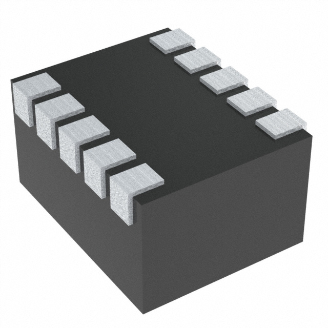
The MAXM17623 and MAXM17624 modules are available in a low profile, compact 10-pin, 2.6mm x 2.1mm x
1.3mm, uSLIC™ package.
2.9V to 5.5V, 1A Himalaya uSLIC
Step-Down Power Modules
Benefits and Features
●● Easy to Use
• 2.9V to 5.5V Input
• Adjustable 0.8V to 3.3V Output
• ±1% Feedback Accuracy
• Up to 1A Output Current
• Fixed 2MHz or 4MHz Operation
• 100% Duty-Cycle Operation
• Internally Compensated
• All Ceramic Capacitors
●● High Efficiency
• Selectable PWM- or PFM-Mode of Operation
• Shutdown Current as Low as 0.1μA (typ)
●● Flexible Design
• Internal Soft-Start and Prebias Startup
• Open-Drain Power Good Output (PGOOD Pin)
●● Robust Operation
• Overtemperature Protection
• -40°C to +125°C Ambient Operating Temperature/
-40°C to +150°C Junction Temperature
●● Rugged
• Passes Drop, Shock, and Vibration Standards:
JESD22-B103, B104, B111
Typical Application Circuit
Applications
●●
●●
●●
●●
●●
Point of Load Power Supply
Standard 5V Rail Supplies
Battery Powered Applications
Distributed Power Systems
Industrial Sensors and Process Control
Ordering Information appears at end of data sheet.
19-100317; Rev 3; 1/20
VIN
2.9V TO 5.5V
CIN
2.2µF
MAXM17624
IN
EN
PGOOD
OUTSNS
OUT
PGND
MODE
FB
SGND
LX
1.5V, 1A
COUT
10µF
VOUT
R1
33.2kΩ
R2
37.4kΩ
�MAXM17623/MAXM17624
2.9V to 5.5V, 1A Himalaya uSLIC
Step-Down Power Modules
Absolute Maximum Ratings
IN to PGND................................................................-0.3V to 6V
EN, PGOOD, FB, OUTSNS to SGND........................-0.3V to 6V
MODE TO SGND..........................................-0.3V to (IN + 0.3V)
LX, OUT TO PGND.......................................-0.3V to (IN + 0.3V)
PGND TO SGND.....................................................-0.3V to 0.3V
Output Short-Circuit Duration.....................................Continuous
Junction Temperature (Note1)..........................................+150°C
Storage Temperature Range................................-55°C to 125°C
Lead Temperature (soldering,10s)...................................+260°C
Soldering Temperature (reflow).......................................+260°C
Stresses beyond those listed under “Absolute Maximum Ratings” may cause permanent damage to the device. These are stress ratings only, and functional operation of the device at these
or any other conditions beyond those indicated in the operational sections of the specifications is not implied. Exposure to absolute maximum rating conditions for extended periods may affect
device reliability.
Package Information
PACKAGE TYPE: 10-PIN uSIP
Package Code
MA102A2+1
Outline Number
21-100245
Land Pattern Number
90-100084
THERMAL RESISTANCE, FOUR-LAYER BOARD (Note 2)
Junction to Ambient (θJA)
77°C/W
For the latest package outline information and land patterns (footprints), go to www.maximintegrated.com/packages. Note that a “+”,
“#”, or “-” in the package code indicates RoHS status only. Package drawings may show a different suffix character, but the drawing
pertains to the package regardless of RoHS status.
Note 1: Junction temperature greater than +125°C degrades operating lifetimes.
Note 2: Package thermal resistance is measured on an evaluation board with natural convection.
Electrical Characteristics
(VIN = VEN = 3.6V, VSGND = VPGND = VMODE = VFB = VOUTSNS = 0V, LX = OUT = PGOOD = OPEN, TA = TJ = -40°C to +125°C,
unless otherwise noted. Typical values are at TA = +25°C. All voltages are referenced to SGND, unless otherwise noted.) (Note 3)
PARAMETER
SYMBOL
CONDITIONS
MIN
TYP
MAX
UNITS
5.5
V
INPUT SUPPLY (VIN)
Input Voltage Range
VIN
IIN-SHDN
Input Supply Current
IQ-PFM
IQ-PWM
Undervoltage Lockout
Threshold (UVLO)
UVLO Hysteresis
www.maximintegrated.com
VIN_UVLO
VIN_UVLO_HYS
2.9
VEN = 0, Shutdown mode
0.1
PFM Mode, No Load
40.0
PWM Mode, MAXM17623
4.5
PWM Mode, MAXM17624
6.0
IN Rising
2.72
2.80
200
µA
mA
2.88
V
mV
Maxim Integrated │ 2
�MAXM17623/MAXM17624
2.9V to 5.5V, 1A Himalaya uSLIC
Step-Down Power Modules
Electrical Characteristics (continued)
(VIN = VEN = 3.6V, VSGND = VPGND = VMODE = VFB = VOUTSNS = 0V, LX = OUT = PGOOD = OPEN, TA = TJ = -40°C to +125°C,
unless otherwise noted. Typical values are at TA = +25°C. All voltages are referenced to SGND, unless otherwise noted.) (Note 3)
PARAMETER
SYMBOL
CONDITIONS
MIN
TYP
MAX
UNITS
0.8
V
ENABLE (EN)
EN Low Threshold
VEN_LOW
EN Falling
EN High Threshold
VEN_HIGH
EN Rising
EN Input Leakage
IEN
EN = 5.5V, TA = TJ =
2
25°C
V
10
50
nA
TIMING
Switching Frequency
Minimum ON time
Maximum Duty Cycle
Soft-Start time
fSW
MAXM17623
1.92
2.00
2.08
MAXM17624
3.84
4.00
4.16
tON_MIN
40
DMAX
MHz
ns
100
%
tSS
1
ms
VFB-REG
0.8
V
FEEDBACK (FB)
FB Regulation Voltage
FB Voltage Accuracy
VFB
PWM Mode
FB Input Bias Current
IFB
FB = 0.6V, TA = TJ = 25°C
50
nA
IOUTSNS-BIAS
VOUTSNS = 1.8V
10
μA
PGOOD Rising Threshold
VPGOOD_RISE
FB Rising
91.5
93.5
95.5
%
PGOOD Falling Threshold
VPGOOD_FALL
FB Falling
88
90
92
%
IPGOOD = 5mA
200
mV
PGOOD = 5.5V, TA = TJ = 25°C
100
nA
OUTSNS Input Bias Current
-1
+1
%
POWER GOOD (PGOOD)
PGOOD Output Low
PGOOD Output Leakage
Current
VOL_PGOOD
ILEAK_PGOOD
PGOOD Deassertion After
Soft-Start
184
μs
5
μA
Thermal Shutdown Rising
Threshold
165
°C
Thermal Shutdown Hysteresis
10
°C
MODE
MODE Pullup Current
VMODE = GND
THERMAL SHUTDOWN
Note 3: Electrical specifications are production tested at TA = +25°C. Specifications over the entire operating temperature range are
guaranteed by design and characterization.
www.maximintegrated.com
Maxim Integrated │ 3
�MAXM17623/MAXM17624
2.9V to 5.5V, 1A Himalaya uSLIC
Step-Down Power Modules
Typical Operating Characteristics
(VIN = VEN = 5V, VSGND = VPGND = VMODE = VFB = VOUTSNS = 0V, LX = OUT = PGOOD = OPEN, TA = TJ = -40°C to +125°C, unless
otherwise noted. Typical values are at TA = +25°C. All voltages are referenced to SGND, unless otherwise noted. The circuit values for
different output voltage applications are as in Table 1, unless otherwise noted.)
MAXM17623 EFFICIENCY vs. LOAD CURRENT
(VOUT = 0.8V, PWM AND PFM MODE)
MAXM17623 EFFICIENCY vs. LOAD CURRENT
(VOUT = 1.2V, PWM AND PFM MODE)
toc01
100
toc02
100
VIN = 3.3V, PWM MODE
VIN = 5V, PWM MODE
VIN = 5V, PWM MODE
0.1
60
1
60
0.01
0.1
1
0.01
LOAD CURRENT (A)
MAXM17624 EFFICIENCY vs. LOAD CURRENT
(VOUT = 1.8V, PWM AND PFM MODE)
100
VIN = 3.3V, PFM MODE
VIN = 5V, PFM MODE
90
EFFICIENCY (%)
VIN = 3.3V, PWM MODE
70
1
toc06
100
toc05
VIN = 5V, PFM MODE
VIN = 3.3V, PFM MODE
VIN = 5V, PFM MODE
90
90
80
0.1
LOAD CURRENT (A)
MAXM17624 EFFICIENCY vs. LOAD CURRENT
(VOUT = 3.3V, PWM AND PFM MODE)
MAXM17624 EFFICIENCY vs. LOAD CURRENT
(VOUT = 2.5V, PWM AND PFM MODE)
toc04
100
80
70
70
VIN = 5V, PWM MODE
0.01
EFFICIENCY (%)
VIN = 3.3V, PWM MODE
EFFICIENCY (%)
EFFICIENCY (%)
EFFICIENCY (%)
VIN = 3.3V, PWM MODE
80
LOAD CURRENT (A)
EFFICIENCY (%)
90
90
80
60
VIN = 3.3V, PFM MODE
VIN = 5V, PFM MODE
VIN = 5V, PFM MODE
VIN = 5V, PFM MODE
70
toc03
100
VIN = 3.3V, PFM MODE
VIN = 3.3V, PFM MODE
90
MAXM17623 EFFICIENCY vs. LOAD CURRENT
(VOUT = 1.5V, PWM AND PFM MODE)
80
VIN = 3.3V, PWM MODE
VIN = 5V, PWM MODE
80
70
70
VIN = 5V, PWM MODE
VIN = 5V, PWM MODE
0.01
0.1
LOAD CURRENT (A)
60
1
MAXM17623 OUTPUT VOLTAGE vs. LOAD CURRENT
(VOUT = 0.8V, PWM AND PFM MODE)
OUTPUT VOLTAGE (V)
OUTPUT VOLTAGE (V)
0.804
VIN = 5V, PWM MODE
0.801
0.798
VIN = 5V, PFM MODE
VIN = 5V, PWM MODE
0.1
LOAD CURRENT (A)
www.maximintegrated.com
1
toc09
1.505
VIN = 3.3V, PFM MODE
1.501
1.499
VIN = 5V, PFM MODE
VIN = 5V, PWM MODE
1.497
1.208
VIN = 3.3V, PFM MODE
0.1
LOAD CURRENT (A)
1.503
1.214
1.211
0.01
MAXM17623 OUTPUT VOLTAGE vs. LOAD CURRENT
(VOUT = 1.5V, PWM AND PFM MODE)
1.217
VIN = 3.3V, PWM MODE
VIN = 3.3V, PWM MODE
0.795
0.01
1
toc08
1.220
0.807
VIN = 5V, PFM MODE
60
0.1
LOAD CURRENT (A)
MAXM17623 OUTPUT VOLTAGE vs. LOAD CURRENT
(VOUT = 1.2V, PWM AND PFM MODE)
toc07
0.810
0.01
OUTPUT VOLTAGE (V)
60
1
1.205
0.01
VIN = 3.3V, PFM MODE
0.1
LOAD CURRENT (A)
1
VIN = 3.3V, PWM MODE
1.495
0.01
0.1
1
LOAD CURRENT (A)
Maxim Integrated │ 4
�MAXM17623/MAXM17624
2.9V to 5.5V, 1A Himalaya uSLIC
Step-Down Power Modules
Typical Operating Characteristics (continued)
(VIN = VEN = 5V, VSGND = VPGND = VMODE = VFB = VOUTSNS = 0V, LX = OUT = PGOOD = OPEN, TA = TJ = -40°C to +125°C, unless
otherwise noted. Typical values are at TA = +25°C. All voltages are referenced to SGND, unless otherwise noted. The circuit values for
different output voltage applications are as in Table 1, unless otherwise noted.)
MAXM17624 OUTPUT VOLTAGE vs. LOAD CURRENT
(VOUT = 1.8V, PWM AND PFM MODE)
MAXM17624 OUTPUT VOLTAGE vs. LOAD CURRENT
(VOUT = 2.5V, PWM AND PFM MODE)
toc10
toc11
2.535
VIN = 5V, PFM MODE
OUTPUT VOLTAGE (V)
OUTPUT VOLTAGE (V)
1.807
1.804
VIN = 3.3V, PFM MODE
1.801
2.532
3.330
VIN = 3.3V, PFM MODE
2.529
2.526
VIN = 5V, PWM MODE
VIN = 5V, PWM MODE
1.798
2.523
VIN = 3.3V, PWM MODE
1.795
0.01
0.1
toc12
3.335
VIN = 5V, PFM MODE
OUTPUT VOLTAGE (V)
1.81
MAXM17624 OUTPUT VOLTAGE vs. LOAD CURRENT
(VOUT = 3.3V, PWM AND PFM MODE)
2.52
1
VIN = 5V, PFM MODE
3.325
3.320
3.315
VIN = 5V, PWM MODE
VIN = 3.3V, PWM MODE
0.01
LOAD CURRENT (A)
0.1
3.310
0.01
1
LOAD CURRENT (A)
MAXM17623 LOAD TRANSIENT RESPONSE
(VIN = 3.3V, VOUT = 0.8V, PWM MODE)
(LOAD CURRENT STEPPED FROM 0.5A TO 1A)
MAXM17623 LOAD TRANSIENT RESPONSE
(VIN = 3.3V, VOUT = 0.8V, PWM MODE)
(LOAD CURRENT STEPPED FROM 0A TO 0.5A)
VOUT
(AC)
20mV/div
IOUT
500mA/div
1
MAXM17623 LOAD TRANSIENT RESPONSE
(VIN = 3.3V, VOUT = 0.8V, PFM MODE)
(LOAD CURRENT STEPPED FROM 0A TO 0.5A)
toc14
toc13
0.1
LOAD CURRENT (A)
VOUT
(AC)
toc15
20mV/div
VOUT(
AC)
20mV/div
500mA/div
IOUT
IOUT
500mA/div
40µs/div
40µs/div
100µs/div
MAXM17623 LOAD TRANSIENT RESPONSE
(VIN = 5V, VOUT = 0.8V, PWM MODE)
(LOAD CURRENT STEPPED FROM 0A TO 0.5A)
MAXM17623 LOAD TRANSIENT RESPONSE
(VIN = 5V, VOUT = 0.8V, PWM MODE)
(LOAD CURRENT STEPPED FROM 0.5A TO 1A)
MAXM17623 LOAD TRANSIENT RESPONSE
(VIN = 5V, VOUT = 0.8V, PFM MODE)
(LOAD CURRENT STEPPED FROM 0A TO 0.5A)
toc17
toc16
VOUT(
AC)
20mV/div
VOUT(
AC)
toc18
20mV/div
VOUT
(AC)
20mV/div
500mA/div
IOUT
500mA/div
40µs/div
www.maximintegrated.com
IOUT
IOUT
40µs/div
500mA/div
100µs/div
Maxim Integrated │ 5
�MAXM17623/MAXM17624
2.9V to 5.5V, 1A Himalaya uSLIC
Step-Down Power Modules
Typical Operating Characteristics (continued)
(VIN = VEN = 5V, VSGND = VPGND = VMODE = VFB = VOUTSNS = 0V, LX = OUT = PGOOD = OPEN, TA = TJ = -40°C to +125°C, unless
otherwise noted. Typical values are at TA = +25°C. All voltages are referenced to SGND, unless otherwise noted. The circuit values for
different output voltage applications are as in Table 1, unless otherwise noted.)
MAXM17623 LOAD TRANSIENT RESPONSE
(VIN = 5V, VOUT = 1.5V, PWM MODE)
(LOAD CURRENT STEPPED FROM 0A TO 0.5A)
MAXM17623 LOAD TRANSIENT RESPONSE
(VIN = 5V, VOUT = 1.5V, PWM MODE)
(LOAD CURRENT STEPPED FROM 0.5A TO 1A)
toc19
MAXM17623 LOAD TRANSIENT RESPONSE
(VIN = 5V, VOUT = 1.5V, PFM MODE)
(LOAD CURRENT STEPPED FROM 0A TO 0.5A)
toc21
toc20
VOUT
(AC)
50mV/div
VOUT
(AC)
IOUT
500mA/div
IOUT
50mV/div
VOUT
(AC)
50mV/div
500mA/div
IOUT
MAXM17624 LOAD TRANSIENT RESPONSE
(VIN = 5V, VOUT = 3.3V, PWM MODE)
(LOAD CURRENT STEPPED FROM 0.5A TO 1A)
MAXM17624 LOAD TRANSIENT RESPONSE
(VIN = 5V, VOUT = 3.3V, PWM MODE)
(LOAD CURRENT STEPPED FROM 0A TO 0.5A)
toc23
toc22
VOUT(
AC)
100µs/div
40µs/div
40µs/div
50mV/div
500mA/div
VOUT
(AC)
MAXM17624 LOAD TRANSIENT RESPONSE
(VIN = 5V, VOUT = 3.3V, PFM MODE)
(LOAD CURRENT STEPPED FROM 30mA TO 530mA)
toc24
50mV/div
VOUT
(AC)
100mV/div
500mA/div
IOUT
500mA/div
IOUT
IOUT
40µs/div
40µs/div
MAXM17623 STARTUP THROUGH ENABLE
(VIN = 5V, VOUT = 0.8V, ILOAD = 0A, PWM MODE)
40µs/div
MAXM17623 STARTUP THROUGH ENABLE
(VIN = 5V, VOUT = 0.8V, ILOAD = 1A, PWM MODE)
toc25
MAXM17624 STARTUP THROUGH ENABLE
(VIN = 5V, VOUT = 3.3V, ILOAD = 0A, PWM MODE)
toc26
5V/div
EN
toc27
5V/div
EN
5V/div
LX
5V/div
PGOOD
5V/div
LX
500mV/div
5V/div
VOUT
PGOOD
200µs/div
www.maximintegrated.com
5V/div
EN
500mV/div
VOUT
500mA/div
LX
5V/div
2V/div
VOUT
5V/div
PGOOD
200µs/div
200µs/div
Maxim Integrated │ 6
�MAXM17623/MAXM17624
2.9V to 5.5V, 1A Himalaya uSLIC
Step-Down Power Modules
Typical Operating Characteristics (continued)
(VIN = VEN = 5V, VSGND = VPGND = VMODE = VFB = VOUTSNS = 0V, LX = OUT = PGOOD = OPEN, TA = TJ = -40°C to +125°C, unless
otherwise noted. Typical values are at TA = +25°C. All voltages are referenced to SGND, unless otherwise noted. The circuit values for
different output voltage applications are as in Table 1, unless otherwise noted.)
MAXM17623 SHUTDOWN THROUGH ENABLE
(VIN = 5V, VOUT = 0.8V, ILOAD = 0A, PWM MODE)
MAXM17624 STARTUP THROUGH ENABLE
(VIN = 5V, VOUT = 3.3V, ILOAD = 1A, PWM MODE)
toc28
MAXM17623 SHUTDOWN THROUGH ENABLE
(VIN = 5V, VOUT = 0.8V, ILOAD = 1A, PWM MODE)
toc29
toc30
5V/div
EN
EN
5V/div
EN
5V/div
5V/div
LX
5V/div
LX
5V/div
2V/div
LX
VOUT
5V/div
VOUT
500mV/div
PGOOD
PGOOD
5V/div
VOUT
4ms/div
200µs/div
MAXM17624 SHUTDOWN THROUGH ENABLE
(VIN = 5V, VOUT = 3.3V, ILOAD = 0A, PWM MODE)
5V/div
10µs/div
MAXM17624 SHUTDOWN THROUGH ENABLE
(VIN = 5V, VOUT = 3.3V, ILOAD = 1A, PWM MODE)
toc31
500mV/div
PGOOD
MAXM17623 STARTUP THROUGH IN
(VIN = 5V, VOUT = 0.8V, ILOAD = 0A, PWM MODE)
toc33
toc32
5V/div
EN
5V/div
EN
5V/div
IN
LX
5V/div
LX
5V/div
LX
VOUT
2V/div
VOUT
2V/div
5V/div
PGOOD
PGOOD
2ms/div
5V/div
MAXM17624 STARTUP THROUGH IN
(VIN = 5V, VOUT = 3.3V, ILOAD = 1A, PWM MODE)
toc35
toc36
5V/div
5V/div
IN
IN
5V/div
500mV/div
VOUT
5V/div
200µs/div
www.maximintegrated.com
5V/div
IN
LX
5V/div
2V/div
LX
5V/div
2V/div
VOUT
5V/div
VOUT
5V/div
PGOOD
PGOOD
5V/div
200µs/div
MAXM17624 STARTUP THROUGH IN
(VIN = 5V, VOUT = 3.3V, ILOAD = 0A, PWM MODE)
toc34
LX
VOUT
PGOOD
20µs/div
MAXM17623 STARTUP THROUGH IN
(VIN = 5V, VOUT = 0.8V, ILOAD = 1A, PWM MODE)
5V/div
500mV/div
PGOOD
200µs/div
200µs/div
Maxim Integrated │ 7
�MAXM17623/MAXM17624
2.9V to 5.5V, 1A Himalaya uSLIC
Step-Down Power Modules
Typical Operating Characteristics (continued)
(VIN = VEN = 5V, VSGND = VPGND = VMODE = VFB = VOUTSNS = 0V, LX = OUT = PGOOD = OPEN, TA = TJ = -40°C to +125°C, unless
otherwise noted. Typical values are at TA = +25°C. All voltages are referenced to SGND, unless otherwise noted. The circuit values for
different output voltage applications are as in Table 1, unless otherwise noted.)
LX
VOUT
5V/div
IN
5V/div
IN
5V/div
5V/div
LX
5V/div
LX
5V/div
500mV/div
PGOOD
toc39
toc38
toc37
IN
MAXM17624 SHUTDOWN THROUGH IN
(VIN = 5V, VOUT = 3.3V, ILOAD = 0A, PWM MODE)
MAXM17623 SHUTDOWN THROUGH IN
(VIN = 5V, VOUT = 0.8V, ILOAD = 0A, PWM MODE)
MAXM17623 SHUTDOWN THROUGH IN
(VIN = 5V, VOUT = 0.8V, ILOAD = 1A, PWM MODE)
5V/div
VOUT
500mV/div
5V/div
PGOOD
VOUT
2V/div
PGOOD
5V/div
10ms/div
20µs/div
2ms/div
MAXM17623 PERMANENT OUTPUT SHORT
(VIN = 5V, VOUT = 0.8V, ILOAD = 1A, PWM MODE)
MAXM17624 SHUTDOWN THROUGH IN
(VIN = 5V, VOUT = 3.3V, ILOAD = 1A, PWM MODE)
toc41
toc40
5V/div
LX
5V/div
VOUT
2V/div
PGOOD
5V/div
toc42
5V/div
SHORT
IN
MAXM17623 PERMANENT OUTPUT SHORT
(VIN = 5V, VOUT = 1.5V, ILOAD = 1A, PWM MODE)
5V/div
SHORT
500mV/div
VOUT
VOUT
1V/div
VLX
5V/div
VLX
5V/div
IOUT
1A/div
IOUT
1A/div
40µs/div
4µs/div
4µs/div
MAXM17624 PERMANENT OUTPUT SHORT
(VIN = 5V, VOUT = 3.3V, ILOAD = 1A, PWM MODE)
MAXM17623 TEMPORARY OUTPUT SHORT
(VIN = 5V, VOUT = 0.8V, ILOAD = 1A, PWM MODE)
toc43
toc44
5V/div
5V/div
500mV/div
SHORT
SHORT
VOUT
2V/div
VOUT
VLX
5V/div
VLX
IOUT
1A/div
IOUT
5V/div
1A/div
4µs/div
www.maximintegrated.com
100µs/div
Maxim Integrated │ 8
�MAXM17623/MAXM17624
2.9V to 5.5V, 1A Himalaya uSLIC
Step-Down Power Modules
Typical Operating Characteristics (continued)
(VIN = VEN = 5V, VSGND = VPGND = VMODE = VFB = VOUTSNS = 0V, LX = OUT = PGOOD = OPEN, TA = TJ = -40°C to +125°C, unless
otherwise noted. Typical values are at TA = +25°C. All voltages are referenced to SGND, unless otherwise noted. The circuit values for
different output voltage applications are as in Table 1, unless otherwise noted.)
MAXM17623 TEMPORARY OUTPUT SHORT
(VIN = 5V, VOUT = 1.5V, ILOAD = 1A, PWM MODE)
MAXM17624 TEMPORARY OUTPUT SHORT
(VIN = 5V, VOUT = 3.3V, ILOAD = 1A, PWM MODE)
toc45
toc46
5V/div
SHORT
SHORT
5V/div
2V/div
1V/div
VOUT
VOUT
VLX
5V/div
VLX
5V/div
1A/div
1A/div
IOUT
IOUT
100µs/div
100µs/div
MAXM17623 BODE PLOT
(VIN = 3.3V, VOUT = 0.8V, FULL LOAD, PWM MODE)
toc48
50
40
160
40
160
30
120
30
120
20
80
10
40
MAGNITUDE
0
PHASE
-10
-40
20
80
10
-40
-20
-30
-120
-30
-40
-160
-40
-80
-120
CROSSOVER FREQUENCY = 198.339kHz
PHASE MARGIN = 53.210°
-50
1000
10000
100000
-160
-200
1000000
FREQUENCY (Hz)
FREQUENCY (Hz)
MAXM17623 BODE PLOT
(VIN = 3.3V, VOUT = 1.5V, FULL LOAD, PWM MODE)
toc49
MAXM17623 BODE PLOT
(VIN = 5V, VOUT = 1.5V, FULL LOAD, PWM MODE)
toc50
50
40
160
40
160
30
120
30
120
20
80
20
80
10
40
MAGNITUDE
0
-10
0
PHASE
-40
GAIN MAGNITUDE (dB)
200
GAIN PHASE (º)
GAIN MAGNITUDE (dB)
0
PHASE
-10
-80
50
40
MAGNITUDE
0
-20
CROSSOVER FREQUENCY = 183.920kHz
PHASE MARGIN = 53.103°
-50
-200
1000
10000
100000
1000000
200
10
-30
-120
-30
-160
-40
-50
1000
10000
100000
FREQUENCY (Hz)
www.maximintegrated.com
-200
1000000
-40
-20
-80
CROSSOVER FREQUENCY = 103.821kHz
PHASE MARGIN = 60.112°
0
PHASE
-10
-20
-40
40
MAGNITUDE
0
200
GAIN PHASE (º)
0
GAIN MAGNITUDE (dB)
200
GAIN PHASE (O)
GAIN MAGNITUDE (dB)
50
MAXM17623 BODE PLOT
(VIN = 5V, VOUT = 0.8V, FULL LOAD, PWM MODE)
GAIN PHASE (º)
toc47
-80
-120
CROSSOVER FREQUENCY = 110.239kHz
PHASE MARGIN = 55.713°
-50
1000
10000
100000
-160
-200
1000000
FREQUENCY (Hz)
Maxim Integrated │ 9
�MAXM17623/MAXM17624
2.9V to 5.5V, 1A Himalaya uSLIC
Step-Down Power Modules
Typical Operating Characteristics (continued)
(VIN = VEN = 5V, VSGND = VPGND = VMODE = VFB = VOUTSNS = 0V, LX = OUT = PGOOD = OPEN, TA = TJ = -40°C to +125°C, unless
otherwise noted. Typical values are at TA = +25°C. All voltages are referenced to SGND, unless otherwise noted. The circuit values for
different output voltage applications are as in Table 1, unless otherwise noted.)
MAXM17623
OUTPUT CURRENT vs. AMBIENT TEMPERATURE
(VIN = 3.3V)
MAXM17624 BODE PLOT
(VIN = 5V, VOUT = 3.3V, FULL LOAD, PWM MODE)
toc51
200
160
30
120
20
80
10
40
MAGNITUDE
0
0
PHASE
-10
-40
-20
-80
-30
-120
toc52
1.2
1.0
LOAD CURRENT (A)
40
GAIN PHASE (º)
GAIN MAGNITUDE (dB)
50
0.8
0.6
VOUT = 1.5V
0.4
VOUT = 0.8V
0.2
CROSSOVER FREQUENCY = 123.829kHz
-160
PHASE MARGIN = 63.213°
-200
-50
1000
10000
100000
1000000
-40
0.0
25
FREQUENCY (Hz)
toc53
1.2
85
105
125
toc54
1.2
1.0
LOAD CURRENT (A)
1.0
LOAD CURRENT (A)
65
MAXM17624 OUTPUT CURRENT
vs. AMBIENT TEMPERATURE
(VIN = 5V)
MAXM17623
OUTPUT CURRENT vs. AMBIENT TEMPERATURE
(VIN = 5V)
VOUT = 1.5V
0.8
VOUT = 0.8V
0.6
0.4
0.8
VOUT = 3.3V
0.6
0.4
0.2
0.0
45
AMBIENT TEMPERATURE (oC)
0.2
25
45
65
85
105
125
0.0
AMBIENT TEMPERATURE (oC)
45
65
85
105
125
AMBIENT TEMPERATURE (oC)
MAXM17624 STARTUP INTO PREBIAS
(VIN = 5V, VPREBIAS = 2.5V, VOUT = 3.3V,
FULL LOAD, PWM MODE)
MAXM17623 STARTUP INTO PREBIAS
(VIN = 5V, VPREBIAS = 0.8V, VOUT = 1.5V,
FULL LOAD, PWM MODE)
toc55
EN
25
toc56
5V/div
500mV/div
5V/div
EN
2V/div
VOUT
VOUT
2V/div
2V/div
LX
LX
5V/div
200µs/div
www.maximintegrated.com
5V/div
PGOOD
PGOOD
200µs/div
Maxim Integrated │ 10
�MAXM17623/MAXM17624
2.9V to 5.5V, 1A Himalaya uSLIC
Step-Down Power Modules
Pin Configuration
TOP VIEW
LX
1
10
IN
OUTSNS
2
9
PGND
FB
3
8
SGND
PGOOD
4
7
EN
MODE
5
6
OUT
MAXM17623/
MAXM17624
INDICATES PIN 1 OF THE MODULE
Pin Description
PIN
NAME
1
LX
2
OUTSNS
3
FB
FUNCTION
Switching Node of the Inductor. No external connection.
Sense Pin for Module VOUT. Connect to the positive terminal of the output capacitor COUT through a
kelvin connection.
Output Feedback Connection. Connect FB to the center of the external resistor-divider from OUT to
SGND to set the output voltage.
Open-Drain Power Good Output. Connect the PGOOD pin to the IN pin through an external pullup
resistor to generate a “high” level if the output voltage is above 93.5% of the target regulated voltage.
If not used, leave this pin unconnected. The PGOOD is driven low if the output voltage is below 90%
of the target regulated voltage.
4
PGOOD
5
MODE
6
OUT
7
EN
8
SGND
Signal GND Pin
9
PGND
Power Ground Pin of the Converter. Connect externally to the power ground plane. Connect
the SGND and PGND pins together at the ground return path of the VIN bypass capacitor. Refer
to the MAXM17623/MAXM17624 Evaluation Kit data sheet for a layout example.
10
IN
www.maximintegrated.com
PWM or PFM Mode Selection Input. Connect the MODE pin to SGND to enable PWM-mode operation. Leave the MODE pin unconnected to enable PFM mode operation.
Module Output Pin. Connect the output capacitor COUT from OUT to PGND.
Enable Input. Logic-high voltage on the EN pin enables the device, while logic-low voltage disables
the device.
Power-Supply Input. Decouple the IN pin to PGND with a capacitor; place the capacitor close to the
IN and PGND pin.
Maxim Integrated │ 11
�MAXM17623/MAXM17624
2.9V to 5.5V, 1A Himalaya uSLIC
Step-Down Power Modules
Functional Diagram
Internal Diagram
MAXM17623/
MAXM17624
IN
HIGH-SIDE
DRIVER
+
EN
2V/0.8V
LX
1.5µH/
1µH
OSCILLATOR
CONTROLLER
OUT
LOW-SIDE
DRIVER
SOFT-START
SGND
OUTSNS
CONTROLLER
MODE LOGIC
PGND
MODE
MODE
SELECTION
LOGIC
FB
www.maximintegrated.com
SLOPE
COMPENSATION
PGOOD
LOGIC
PGOOD
Maxim Integrated │ 12
�MAXM17623/MAXM17624
Detailed Description
MAXM17623 and MAXM17624 are high-frequency synchronous step down DC-DC converter modules, with
integrated MOSFETs, compensation components, and
inductors, that operate over a 2.9V to 5.5V input voltage
range. MAXM17623 and MAXM17624 support up to 1A
load current and allow use of small, low cost input and
output capacitors. The output voltage can be adjusted
from 0.8V to 3.3V.
When the EN pin is asserted, an internal power-up
sequence ramps up the error-amplifier reference, resulting in output-voltage soft-start. The FB pin monitors the
output voltage through a resistor-divider. The devices
select either PFM or forced-PWM mode depending on the
state of the MODE pin at power-up. By pulling the EN pin
to low, the devices enter shutdown mode and consume
only 0.1μA (typ) of standby current.
The modules use an internally compensated, fixedfrequency, peak-current mode control scheme. On the
falling edge of an internal clock, the high-side pMOSFET
turns on, and continues to be on during normal operation
until at least the rising edge of the clock (for 40ns). An
internal error amplifier compares the feedback voltage
to a fixed internal reference voltage and generates an
error voltage. The error voltage is compared to a sum
of the current-sense voltage and a slope-compensation
voltage by a PWM comparator to set the on-time. During
the on-time of the pMOSFET, the inductor current ramps
up. For the remainder of the switching period (off-time),
the pMOSFET is kept off and the low-side nMOSFET
turns on. During the off-time, the inductor releases the
stored energy as the inductor current ramps down, providing current to the output. Under overload conditions,
the cycle-by-cycle current-limit feature limits the inductor
peak current by turning off the high-side pMOSFET and
turning on the low-side nMOSFET.
Mode Selection (MODE)
The logic state of the MODE pin is latched after the EN
pin goes above its rising threshold and all internal voltages are ready to allow LX switching. If the MODE pin is
unconnected at power-up, the part operates in PFM mode
at light loads. If the MODE pin is grounded at power-up,
the part operates in constant-frequency PWM mode at all
loads. State changes on the MODE pin are ignored during
normal operation.
www.maximintegrated.com
2.9V to 5.5V, 1A Himalaya uSLIC
Step-Down Power Modules
PWM Mode
In PWM mode, the module output current is allowed to
go negative. PWM operation is useful in frequency sensi
tive applications and provides fixed switching frequency
operation at all loads. However, PWM-mode of operation
gives lower efficiency at light loads compared to PFMmode of operation.
PFM Mode
PFM mode of operation disables negative output current
from the module and skips pulses at light loads for better
efficiency. At low load currents, if the peak value of the
inductor current is less than 350mA for 64 consecutive
cycles, and the inductor current reaches zero, the part
enters PFM mode. In PFM mode, When the FB pin voltage is below 0.8V, the high-side switch is turned-on until
the inductor current reaches 500mA. After the high-side
switch is turned OFF, the low-side switch is turned ON
until the inductor current comes down to zero and LX
enters a high-impedance state. If the FB pin voltage is
greater than 0.8V for 3 consecutive CLK falling edges
after LX enters a high-impedance state, the module continues to operate in PFM mode. In PFM mode, the part
hibernates when the FB pin voltage is above 0.8V for
5 consecutive switching cycles after LX enters a highimpedance state. If the FB pin voltage drops below 0.8V
within 3 consecutive CLK falling edges after LX enters a
high-impedance state, the part comes out of PFM mode.
EN Input (EN), Soft-Start
When EN voltage is above 2V (min), the internal erroramplifier reference voltage starts to ramp up. The duration of the soft-start ramp is 1ms (typ), allowing a smooth
increase of the output voltage. Driving EN low disables
both power MOSFETs, as well as other internal circuitry,
and reduces IN quiescent current to below 0.1μA.
Power Good (PGOOD)
The devices include an open-drain power good output
that indicates the output voltage status. PGOOD goes
high when the output voltage is above 93.5% of the target
value, and goes low when the output voltage is below
90% of the target value. During start-up, the PGOOD pin
goes high after 184μs of soft-start completion.
Startup into a Prebiased Output
The devices are capable of soft-start into a prebiased out
put, without discharging the output capacitor in both the
PFM and forced-PWM modes. Such a feature is useful in
applications where digital integrated circuits with multiple
rails are powered.
Maxim Integrated │ 13
�MAXM17623/MAXM17624
Overcurrent Protection
The MAXM17623/MAXM17624 are provided with a robust
overcurrent protection (OCP) scheme that protects the
modules under overload and output short-circuit conditions. When overcurrent is detected in the inductor, the
switches are controlled by a mechanism, which detects
both the high-side MOSFET and low-side MOSFET
currents and compares them with the respective limits.
Whenever the inductor current exceeds the internal peak
current limit of 1.7A (typ), the high-side MOSFET is turned
OFF and the low-side MOSFET is turned ON. The low
side MOSFET is kept ON until the subsequent CLK rising
edge after the inductor current drops below 1.4A (typ).
The high-side MOSFET is turned ON after the low-side
MOSFET is turned OFF and the cyclic operation continues. When the overload condition is removed, the part
regulates output to the set voltage.
The MAXM17623/MAXM17624 are designed to support a
maximum load current of 1A. The inductor ripple current
is calculates as follows.
For MAXM17623:
∆I
VIN − VOUT − 0.191× I OUT VOUT + 0.236 × I OUT
× V − 0.13 × I
L × f SW
IN
OUT
For MAXM17624:
∆I
VIN − VOUT − 0.157 × I OUT VOUT + 0.202 × I OUT
× V − 0.13 × I
L × f SW
IN
OUT
2.9V to 5.5V, 1A Himalaya uSLIC
Step-Down Power Modules
Thermal Overload Protection
Thermal overload protection limits the total power dis
sipation in the device. When the junction temperature
exceeds +165°C, an on-chip thermal sensor shuts down
the device, turns off the internal power MOSFETs, allow
ing the device to cool down. The thermal sensor turns the
device on after the junction temperature cools by 10°C.
Applications Information
Selection of Input Capacitor
The input filter capacitor reduces peak currents drawn
from the power source and reduces noise and voltage
ripple on the input caused by the circuit’s switching.
The input capacitor RMS current requirement (IRMS) is
defined by the following equation:
=
IRMS I OUT(MAX) ×
VOUT × (VIN − VOUT )
VIN
where IOUT(MAX) is the maximum load current. IRMS has
a maximum value when the input voltage equals twice
the output voltage (VIN = 2 x VOUT), so IRMS(MAX) =
IOUT(MAX)/2.
Choose an input capacitor that exhibits less than +10°C
temperature rise at the RMS input current for optimal
long-term reliability. Use low-ESR ceramic capacitors with
high-ripple-current capability at the input. X7R capacitors
are recommended in industrial applications for their temperature stability. Calculate the input capacitance using
the following equation:
Where:
VOUT = Steady-state output voltage
VIN = Operating input voltage
fSW = Switching Frequency
L = Power module output inductance (1.5μH ±20% for
MAXM17623, 1μH ±20% for MAXM17624)
IOUT = Required output (load) current
The following condition should be satisfied at the desired
load current (IOUT):
=
C IN I OUT(MAX) × D ×
(1 − D)
η × f SW × ∆VIN
where,
D = Duty ratio of the converter
fSW = Switching frequency
∆VIN = Allowable input voltage ripple
η = Efficiency
∆I
IOUT + 2 < 1.8
www.maximintegrated.com
Maxim Integrated │ 14
�MAXM17623/MAXM17624
2.9V to 5.5V, 1A Himalaya uSLIC
Step-Down Power Modules
Selection of Output Capacitor
Small ceramic X7R-grade capacitors are sufficient and
recommended for the device. The output capacitor has
two functions. It filters the square wave generated by the
device along with the internal inductor. It stores sufficient
energy to support the output voltage under load transient
conditions and stabilizes the device’s internal control loop.
Usually the output capacitor is sized to support a step
load of 50% of the maximum output current in the application, such that the output-voltage deviation is less than
3%. Derating of ceramic capacitors with DC-voltage must
be considered while selecting the output capacitor. Refer
to Table 1 for recommended output capacitors.
OUT
MAXM17623/
MAXM17624
R1
FB
R2
Figure 1. Setting the Output Voltage
Adjusting the Output Voltage
The MAXM17623/MAXM17624 output voltage can be
programmed from 0.8V to 3.3V. Set the output voltage by
connecting a resistor-divider from output to FB to GND
(see Figure 2).
LX
Choose R2 to be less than 37.4kΩ and calculate R1 with
the following equation:
V
R1 =
R 2 × OUT − 1
0.8
1
+
MAXM17623/
MAXM17624
10
IN
OUTSNS
2
9
PGND
FB
3
8
SGND
PGOOD
4
7
EN
MODE
5
6
OUT
CIN
COUT
R2
R1
Figure 2. Layout Guidelines
Table 1. Selection of Components
PART NUMBER
V IN(MIN)
(V)
V IN(MAX)
(V)
V OUT (V)
C IN
C OUT
R1
R2
2.9
5.5
0.8
1 x 2.2μF 0603 10V
GRM188R71A225KE15
1 x 22μF 0805 6.3V
GRM21BZ70J226ME44#
0Ω
37.4kΩ
2.9
5.5
1.0
1 x 2.2μF 0603 10V
GRM188R71A225KE15
1 x 22μF 0805 6.3V
GRM21BZ70J226ME44#
9.53kΩ
37.4kΩ
2.9
5.5
1.2
1 x 2.2μF 0603 10V
GRM188R71A225KE15
1 x 22μF 0805 6.3V
GRM21BZ70J226ME44#
19.1kΩ
37.4kΩ
2.9
5.5
1.5
1 x 2.2μF 0603 10V
GRM188R71A225KE15
1 x 22μF 0805 6.3V
GRM21BZ70J226ME44#
33.2kΩ
37.4kΩ
2.9
5.5
1.5
1 x 2.2μF 0603 10V
GRM188R71A225KE15
1 x 10μF 0805 16V
GRM21BZ71C106KE15#
33.2kΩ
37.4kΩ
2.9
5.5
1.8
1 x 2.2μF 0603 10V
GRM188R71A225KE15
1 x 10μF 0805 16V
GRM21BZ71C106KE15#
49.9kΩ
37.4kΩ
2.9
5.5
2.5
1 x 2.2μF 0603 10V
GRM188R71A225KE15
1 x 10μF 0805 16V
GRM21BZ71C106KE15#
86.6kΩ
37.4kΩ
3.6
5.5
3.3
1 x 2.2μF 0603 10V
GRM188R71A225KE15
1 x 10μF 0805 16V
GRM21BZ71C106KE15#
118kΩ
37.4kΩ
MAXM17623
MAXM17624
www.maximintegrated.com
Maxim Integrated │ 15
�MAXM17623/MAXM17624
2.9V to 5.5V, 1A Himalaya uSLIC
Step-Down Power Modules
Power Dissipation
PCB Layout Guidelines
The power dissipation inside the module leads to an
increase in the junction temperature of the MAXM17623
and MAXM17624. The power loss inside the modules at
full load can be estimated as follows:
PLOSS
=
POUT
×
[ 1η − 1]
Where η is the efficiency of the power module at the
desired operating conditions. The junction temperature
TJ of the module can be estimated at any given maximum
ambient temperature TA from the following equation:
TJ = TA + [θJA × PLOSS]
For the MAXM17623/MAXM17624 evaluation board,
the thermal resistance from Junction to Ambient (θJA)
is 77°C/W. Operating the module at Junction temperatures greater than +125°C degrades operating lifetimes.
An EE-SIM model is available for the MAXM17623/
MAXM17624, to simulate efficiency and power loss for the
desired operating conditions.
Careful PCB layout is critical to achieving low switching
losses and clean, stable operation.
Use the following guidelines for good PCB layout:
●● Keep the input capacitors as close as possible to the
IN and PGND pins.
●● Keep the output capacitors as close as possible to
the OUT and PGND pins.
●● Keep the resistive feedback divider as close as possible to the FB pin.
●● Connect all of the PGND connections to a copper
plane area as large as as possible on the top and
bottom layers.
●● Use multiple vias to connect internal PGND planes to
the top layer PGND plane.
●● Keep the power traces and load connections short.
This practice is essential for high efficiency. Using
thick copper PCBs (2oz vs. 1oz) can enhance fullload efficiency. Correctly routing PCB traces is a difficult task that must be approached in terms of fractions of centimeters, where a single mΩ of excess
trace resistance causes a measurable efficiency
penalty.
Typical Application Circuits
Typical Application Circuit (0.8V, 1A)
VIN
2.9V TO 5.5V
CIN
2.2µF
MAXM17623
IN
EN
PGOOD
www.maximintegrated.com
OUTSNS
OUT
PGND
MODE
FB
SGND
LX
0.8V, 1A
COUT
22µF
VOUT
R1
0Ω
R2
37.4kΩ
Maxim Integrated │ 16
�MAXM17623/MAXM17624
2.9V to 5.5V, 1A Himalaya uSLIC
Step-Down Power Modules
Typical Application Circuits (continued)
Typical Application Circuit (1.5V, 1A)
VIN
2.9V TO 5.5V
CIN
2.2µF
MAXM17623
IN
OUTSNS
EN
OUT
PGOOD
PGND
MODE
1.5V, 1A
COUT
22µF
VOUT
R1
33.2kΩ
FB
R2
37.4kΩ
LX
SGND
Typical Application Circuit (1.5V, 1A)
VIN
2.9V TO 5.5V
CIN
2.2µF
MAXM17624
IN
EN
PGOOD
www.maximintegrated.com
OUTSNS
OUT
PGND
MODE
FB
SGND
LX
1.5V, 1A
COUT
10µF
VOUT
R1
33.2kΩ
R2
37.4kΩ
Maxim Integrated │ 17
�MAXM17623/MAXM17624
2.9V to 5.5V, 1A Himalaya uSLIC
Step-Down Power Modules
Typical Application Circuits (continued)
Typical Application Circuit (3.3V, 1A)
VIN
3.6V TO 5.5V
CIN
2.2µF
MAXM17624
IN
EN
PGOOD
MODE
SGND
OUTSNS
OUT
PGND
3.3V, 1A
COUT
10µF
VOUT
R1
118kΩ
FB
LX
R2
37.4kΩ
Ordering Information
PART NUMBER
TEMP RANGE
PIN-PACKAGE
V OUT (V)
MAXM17623AMB+
-40ºC to +125ºC
10-pin 2.6mm x 2.1mm x 1.3mm uSLIC package
0.8 to 1.5
MAXM17623AMB+T
-40ºC to +125ºC
10-pin 2.6mm x 2.1mm x 1.3mm uSLIC package
0.8 to 1.5
MAXM17624AMB+
-40ºC to +125ºC
10-pin 2.6mm x 2.1mm x 1.3mm uSLIC package
1.5 to 3.3
MAXM17624AMB+T
-40ºC to +125ºC
10-pin 2.6mm x 2.1mm x 1.3mm uSLIC package
1.5 to 3.3
+ Denotes a lead(Pb)-free/RoHS-compliant package.
T Denotes tape-and-reel.
www.maximintegrated.com
Maxim Integrated │ 18
�MAXM17623/MAXM17624
2.9V to 5.5V, 1A Himalaya uSLIC
Step-Down Power Modules
Revision History
REVISION
NUMBER
REVISION
DATE
PAGES
CHANGED
DESCRIPTION
0
12/18
Initial release
1
2/19
Updated TOC05, TOC17, and Table 1
4–5, 14
—
2
6/19
Updated the Package Information section, and TOC36 and TOC40; replaced TOC01‒
TOC06 and TOC 46‒TOC48
2, 4, 7–9
3
1/20
Updated the Electrical Characteristics, Typical Operating Characteristics, Pin
Configuration, and Pin Description sections; updated TOC46–TOC50; added new
TOC02, TOC04, TOC05, TOC08, TOC10 and TOC11, and renumbered remaining TOCs
2–10, 17
For pricing, delivery, and ordering information, please visit Maxim Integrated’s online storefront at https://www.maximintegrated.com/en/storefront/storefront.html.
Maxim Integrated cannot assume responsibility for use of any circuitry other than circuitry entirely embodied in a Maxim Integrated product. No circuit patent licenses
are implied. Maxim Integrated reserves the right to change the circuitry and specifications without notice at any time. The parametric values (min and max limits)
shown in the Electrical Characteristics table are guaranteed. Other parametric values quoted in this data sheet are provided for guidance.
Maxim Integrated and the Maxim Integrated logo are trademarks of Maxim Integrated Products, Inc.
© 2020 Maxim Integrated Products, Inc. │ 19
�Mouser Electronics
Authorized Distributor
Click to View Pricing, Inventory, Delivery & Lifecycle Information:
Maxim Integrated:
MAXM17624AMB+T MAXM17623AMB+T
�


 工商网监
湘ICP备2023018690号
工商网监
湘ICP备2023018690号
