Rev 2; 7/05
MAXQ2000 Evaluation Kit
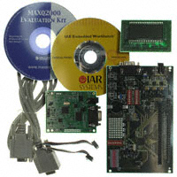
The MAXQ2000 evaluation kit (EV kit) is a proven platform to conveniently evaluate the capabilities of the
MAXQ2000 low-power LCD microcontroller. The kit contains the MAXQ2000 with pins brought out to headers, a
JTAG programming interface, fixed and adjustable
power supplies, a DB-9 serial connector, an LCD display, and switches and LEDs to control and display
board operation. With the included software, serial-toJTAG interface board, and an RS-232 cable connected
to a personal computer, the kit provides a completely
functional system ideal for evaluating the capabilities of
the MAXQ2000.
Evaluation Kit Contents
Features
♦ Easily Loads Code Using Bootstrap Loader and
Serial-to-JTAG Interface Board
♦ JTAG Interface Provides In-Application
Debugging Features
Step-by-Step Execution Tracing
Breakpointing by Code Address, Data Memory
Address, or Register Access
Data Memory View and Edit
♦ Removable, Static, 4-1/2 Digit LCD Display
♦ DB-9 RS-232 Serial Connector and Level
Translator
♦ MAXQ2000 Evaluation Kit Board with Processor
and 13.5MHz Crystal Installed
♦ On-Board 3.6V, 2.5V and Adjustable 1.8V to 3.6V
Power-Supply Regulators
♦ Serial-to-JTAG Interface Board and JTAG Cable
♦ Evaluation Kit Board can be Powered Directly
over JTAG Interface
♦ MAXQ2000 LCD Display Daughterboard
♦ MAXQ2000 Evaluation Kit CD-ROM
♦ Processor Clock can be run from Crystal or
Programmable Oscillator
♦ Serial EEPROM
Ordering Information
PART
DESCRIPTION
MAXQ2000-KIT
MAXQ2000 EV Kit Board
♦ DS2433 1-Wire® EEPROM Demonstrates Use of
1-Wire Interface
♦ MAX1407 ADC/DAC Demonstrates Use of SPI™
Interface
♦ Optional LED Display of Port 0 Logic Levels
♦ Pushbutton Switches for Reset and Interrupt
Generation
♦ 32kHz Crystal for Real-Time Clock Oscillator Use
♦ Prototyping Area Including VDDIO and VDD Voltage
Rails
MAXQ is a registered trademark of Maxim Integrated Products, Inc.
1-Wire is a registered trademark of Dallas Semiconductor Corp.
SPI is a trademark of Motorola, Inc.
♦ Test/Expansion Header Includes All Device GPIO
and LCD Pins
♦ Configuration DIP Switches Connect/Disconnect
All Demonstration Circuitry from Port Pins
♦ Board Schematics Provide a Convenient
Reference Design
______________________________________________ Maxim Integrated Products
For pricing, delivery, and ordering information, please contact Maxim Direct at 1-888-629-4642,
or visit Maxim’s website at www.maxim-ic.com.
1
Evaluates: MAXQ2000
General Description
�MAXQ2000 Evaluation Kit
Evaluates: MAXQ2000
Component List—Evaluation Kit Board
DESIGNATION
QTY
DESCRIPTION
SUPPLIER
C1, C3, C4, C19
4
10µF, 10V tantalum capacitors
Panasonic
ECS-T1AX106R
C2, C5, C6
3
10µF, 16V capacitors (1210)
Panasonic
ECJ3YF1C106Z
C7, C8, C11–C16,
C20–C24
13
100nF 10%, 10V capacitors (0805)
Generic
—
C9, C10
2
10pF 5%, 50V capacitors (0805)
Panasonic
ECJ2VC1H100D
C17
1
18nF 10%, 10V capacitor (0805)
Generic
—
C18
1
4.7µF 10%, 10V capacitor (0805)
Generic
—
JU1, JU2, JU3
3
1 x 3, 0.1” spaced jumpers
3M
929834-02-03
JU4–JU11
8
1 x 2, 0.1” spaced jumpers
3M
929834-02-02
J1
1
Male 2mm power connector
CUI Inc.
PJ-002A
J2
1
2 x 36, 0.1” spaced header
3M
929836-02-36
J3
1
2 x 26, 0.1” spaced header
3M
929836-02-26
J4
1
2 x 5, 0.1” spaced header
3M
929836-02-05
J5
1
Female RS-232 DB9 connector
Amp/Tyco
745781-4
J6
1
DS9094F surface-mount iButton® clip
Dallas Semiconductor
DS9094FS
J7
1
1 x 8, 0.1” spaced header
3M
929834-02-08
RN1
1
1kΩ SIP-9 resistor pack
CTS
770-10-1-102
R1, R4, R5
3
25.5kΩ 1%, 1/8W resistors (0805)
Generic
—
R2
1
50kΩ potentiometer resistor
Panasonic
EVN-D2AA03B54
R3, R6
2
13.0kΩ 1%, 1/8 W resistors (0805)
Generic
—
R7
1
23.7kΩ 1%, 1/8 W resistor (0805)
Generic
—
R8
1
10kΩ potentiometer resistor
Panasonic
EVN-D2AA03B14
R9–R13
5
1kΩ, 1/8W resistors (0805)
Generic
—
R14–R20
7
10kΩ, 1/8 W resistors (0805)
Generic
—
R21
1
Empty resistor footprint (0805)
—
—
SW1, SW3, SW6
3
DIP switches x 8
C&K
SDA08H1KD
SW2, SW4, SW5
3
SPST N/O pushbutton
Omron
B3FS-1000
TP1—TP4
4
1 x 2, 0.100” spaced test points
3M
929834-02-02
U1, U2, U3
3
MAX1658 350mA linear regulator
Maxim
MAX1658ESA
U4
1
MAXQ2000 low-power LCD micro
Maxim
MAXQ2000-RAX
U5
1
DS1077L 3V EconOscillator™
Dallas Semiconductor
DS1077LZ-40
U6
1
MAX3387E 3V RS-232 transceiver
Maxim
MAX3387ExUG
U7
1
DS2433 4kB 1-Wire EEPROM
Dallas Semiconductor
DS2433S
U8
1
MAX1407 16-bit multi-ADC/DAC
Maxim
MAX1407CAI
2
U9
1
AT24C32A 1.8V I C EEPROM
Atmel
AT24C32AN-10SI-1.8
U10
1
74VHC541 octal buffer
Fairchild
74VHC541MTC
U11
1
10-segment bar graph red LED
Fairchild
MV57164
Y1
1
13.5MHz, 18pF crystal
Citizen
HC49US13.500MABJ
Y2, Y3
2
32kHz, 6pF crystals
Epson
C-002RX32.768K-E
iButton is a registered trademark of Dallas Semiconductor Corp.
EconOscillator is a trademark of Dallas Semiconductor Corp.
2
PART
_____________________________________________________________________
�MAXQ2000 Evaluation Kit
DESIGNATION
QTY
C1–C4
4
Empty capacitor footprint (0805)
DESCRIPTION
—
SUPPLIER
—
PART
J1
1
2 x 26, 0.1” spaced socket
3M
929975-01-26
R1–R3
3
Empty resistor footprint (0805)
—
—
U1
1
Static, 3V, 4-1/2 digit display LCD
Varitronix
VI-502-DP-RC-S
Detailed Description
This evaluation kit must be used with the following documents:
• MAXQ2000 Data Sheet
(www.maxim-ic.com/MAXQ2000)
• MAXQ Family User’s Guide
(www.maxim-ic.com/MAXQUG)
• MAXQ Family User’s Guide: MAXQ2000 Supplement
(www.maxim-ic.com/MAXQ2k_sup)
The MAXQ2000 EV kit board and LCD display daughterboard are fully defined in the schematics provided in this
document. However, a short description of the major
components and connectors of the boards follows.
Power Supplies
There are three different ways to set up power supplies
when using the MAXQ2000 EV kit. The two boards that
require power supplies are the MAXQ2000 EV kit board
and the serial-to-JTAG interface board. The LCD
daughterboard simply plugs into the MAXQ2000 EV kit
board and does not require its own power supply.
Two different types of power supplies (which are not
included with the MAXQ2000 EV kit) are required to set
up the configurations listed below.
• 5V, ±5% 300mA DC regulated supply (25mm,
center-post, positive female connector) to power the
serial-to-JTAG interface board.
• 6V to 9V, 300mA DC supply (2.5mm, center-post,
positive female connector) to power the MAXQ2000
EV kit board.
Running Both Boards from
Separate Power Supplies
To run each of the boards from its own power supply,
connect supplies as follows.
• Connect a 5V, ±5% regulated DC wall supply to the
J2 power plug of the serial-to-JTAG interface board.
• Connect a 6V to 9V DC wall supply (center post positive, at least 300mA capacity) to the J1 power plug of
the MAXQ2000 EV kit board.
Note: When using two power supplies in this manner, the JU11 jumper on the MAXQ2000 EV kit board
must be DISCONNECTED.
Running Both Boards from a Single Power Supply
If the serial-to-JTAG interface board is being used, a
single power supply can be used to power both boards
as follows.
• Connect a 5V, ±5% regulated DC wall supply to the
J2 power plug of the serial-to-JTAG interface board.
• Connect the JH3 jumper on the serial-to-JTAG interface board.
• Connect the JU11 jumper on the MAXQ2000 EV kit
board.
Note: Do not connect a power supply to the J1 plug
on the MAXQ2000 EV kit when powering the boards
in this manner.
Running the MAXQ2000 EV KIT Board
from a Single Power Supply
If the MAXQ2000 has already been programmed using
the JTAG interface, it is possible to disconnect the serial-to-JTAG board and power up the MAXQ2000
Evaluation Kit board on its own. This simply executes
the previously loaded firmware, with no possibility of inapplication load or debugging.
• Connect a 6V to 9V DC wall supply (center post positive, at least 300mA capacity) to the J1 power plug of
the MAXQ2000 EV kit board.
_____________________________________________________________________
3
Evaluates: MAXQ2000
Component List—LCD Display Daughterboard
�Evaluates: MAXQ2000
MAXQ2000 Evaluation Kit
Internal Power Rails
Using the LCD Display
The MAXQ2000 EV kit board generates three internal
power rails from the DC input power supply (from J1 or
the serial-to-JTAG board). Each of these supplies may
be used to support up to 100mA of additional circuitry
in the prototyping area. (Note: Test point TP1 is board
ground.)
• The adjustable power supply, which can be measured at test point TP2, provides an adjustable voltage between +1.8V and +3.6V. The level of this
supply can be adjusted manually by turning potentiometer R2 with a screwdriver.
• The 3.6V fixed power supply can be measured at
test point TP3. This voltage level can be used for
VDDIO or VLCD, but not VDD.
• The 2.5V fixed power supply can be measured at
test point TP4. This voltage level can be used for
VDDIO, VLCD, or VDD.
Table 1 shows how the jumpers connect the MAXQ2000
power rails to the on-board power supplies.
To use the LCD daughterboard, it should be installed on
the J3 connector of the MAXQ2000 EV kit board. Pin 1
on J3 should line up with pin 1 of the LCD daughterboard J1 connector. Note that when the LCD daughterboard is installed correctly, it hangs off the top edge of
the MAXQ2000 EV kit board. When the LCD display is in
use, VLCD should be connected to +3.6V.
The LCD display on the LCD daughterboard is a static,
4-1/2 digit display. Figure 4 shows how the segments
are mapped. If the LCD display is not needed, it can be
removed to free up port pins P0.0–P0.7, P1.0–P1.7,
P2.0–P2.7, and P3.0–P3.7 for other uses.
Additional Hardware Features
Most of the additional hardware on the MAXQ2000 EV
kit board, such as the serial port, the MAX1407, and the
1-Wire interface, can be enabled or disabled by setting
jumpers or DIP switches. Disabling unused hardware
frees up the associated port pins for other uses.
Table 1. Power-Supply Jumper Settings
JUMPER
SETTING
EFFECT
JU1
(No jumper)
JU1
Pins 1 and 2 connected
VDD is floating (drive from bench supply)*
JU1
Pins 2 and 3 connected
JU2
(No jumper)
JU2
Pins 1 and 2 connected
JU2
Pins 2 and 3 connected
JU3
(No jumper)
JU3
Pins 1 and 2 connected
VLCD is driven by +3.6V fixed supply
JU3
Pins 2 and 3 connected
VLCD is driven by adjustable supply
VDD is driven by +2.5V fixed supply
VDD is driven by adjustable supply*
VDDIO is floating (drive from bench supply)
VDDIO is driven by +3.6V fixed supply
VDDIO is driven by adjustable supply
VLCD is floating (drive from bench supply)
* Refer to the MAXQ2000 data sheet for the allowable range of the VDD supply.
4
_____________________________________________________________________
�MAXQ2000 Evaluation Kit
Evaluates: MAXQ2000
Table 2. Other Jumper and DIP Switch Settings
JUMPER/
SWITCH
WHEN OPEN/OFF
JU4
HFXIN is driven by the socketed
crystal
JU5
No effect
P6.0 is connected to DS1077 SCL
JU6
No effect
P6.1 is connected to DS1077 SDA
SW1 #1
No effect
RS-232 DTR/CTS connected (loopback test)
SW1 #2
No effect
RS-232 RTS/DSR connected (loopback test)
SW1 #3
No effect
RTS flow control input connected to P5.2
SW1 #4
No effect
Serial receive connected to P7.1 (RXD0)
SW1 #5
No effect
DTR flow control input connected to P5.3
SW1 #6
No effect
DSR flow control output connected to P6.4
SW1 #7
No effect
Serial transmit connected to P7.0 (TXD0)
SW1 #8
No effect
CTS flow control output connected to P6.5
JU7
No effect
DS2433 data line connected to 1-Wire bus
JU8
No effect
P6.2 (OWOUT) connected to 1-Wire bus
JU9
No effect
P6.3 (OWIN) connected to 1-Wire bus
JU10
No effect
HFXADJ is driven by DS1077L output
JU11
Kit board is powered from
J1 supply
Kit board will be powered over JTAG
SW3 #1
No effect
MAX1407 RESET connected to P6.4
SW3 #2
No effect
HFXADJ is driven by MAX1407 FOUT
SW3 #3
No effect
MAX1407 CS connected to P5.4 (SSEL)
SW3 #4
No effect
MAX1407 SCLK connected to P5.6 (SCLK)
SW3 #5
No effect
MAX1407 DIN connected to P5.5 (MOSI)
SW3 #6
No effect
MAX1407 DOUT connected to P5.7 (MISO)
SW3 #7
No effect
MAX1407 INT connected to P6.0
SW3 #8
No effect
MAX1407 DRDY connected to P6.1
SW6 #1
No effect
MAX1407 WU1 connected to P6.5
SW6 #2
No effect
SW4 pulls P5.2 to ground when pressed (Note 1)
SW6 #3
No effect
SW4 pulls P5.3 to ground when pressed (Note 1)
SW6 #4
No effect
SW5 pulls P7.0 to ground when pressed (Note 2)
WHEN CLOSED/ON
HFXIN is connected to HFXADJ
SW6 #5
No effect
SW5 pulls P7.1 to ground when pressed (Note 2)
SW6 #6
No effect
EEPROM SCL connected to P6.0
SW6 #7
No effect
EEPROM SDA connected to P6.1
SW6 #8
No effect
LED bar graph displays Port 0 logic levels
Note 1: If both SW6 #2 and #3 are closed, P5.2 and P5.3 will be shorted together.
Note 2: If both SW6 #4 and #5 are closed, P7.0 and P7.1 will be shorted together.
_____________________________________________________________________
5
�Evaluates: MAXQ2000
MAXQ2000 Evaluation Kit
Figure 1. MAXQ2000 Evaluation Kit Setup
TEST MODE SELECT
TEST CLOCK
WINDOWS
PC
SERIAL-TO-JTAG
INTERFACE
ADAPTER
SERIAL
(COM)
PORT
TEST DATA IN
TEST DATA OUT
RS-232
INTERFACE
JTAG/TAP
INTERFACE
Figure 2. MAXQ2000 Serial-to-JTAG Interface
6
_____________________________________________________________________
MAXQ2000
�MAXQ2000 Evaluation Kit
Evaluates: MAXQ2000
Figure 3. MAXQ2000 Evaluation Kit Functional Layout
Figure 4. LCD Daughterboard Display Memory Mapping
_____________________________________________________________________
7
�8
3
2
1
VPIN
Figure 5. MAXQ2000 Evaluation Kit Power Schematics—Power (1 of 6)
_____________________________________________________________________
2
1
VPIN
C5
10μF
16V
2
7
6
3
U2
GND
8
MAX1658
TP1
GND
SHDN
IN7
IN6
IN3
CENTER POST POSTIVE
5-9 VDC
PJ-002A
G2
G1
IN
J1
2
1
SET
OUT5
OUT4
1
5
4
VP36
VP36
VP25
2
1
2
1
1
1
1
R6
13.0k 1%
R4
25.5k 1%
JU3
2
JU2
2
VDDIO
JU1
2
VDD
3
3
3
2
1
VP36
C3
10μF
10V
2
1
VTEST
VLCD
VTEST
VTEST
TP3
+3.6V
2
1
VPIN
2
1
VPIN
C6
10μF
16V
C2
10μF
16V
2
7
6
3
2
7
6
3
SHDN
IN7
IN6
IN3
SHDN
IN7
IN6
IN3
1
GND
8
MAX1658
U3
GND
8
MAX1658
U1
SET
OUT5
OUT4
1
5
4
2
1
5
4
R3
13.0k 1%
SET
OUT5
OUT4
2
1
2
1
3
1
2
1
1
R7
23.7k 1%
R5
25.5k 1%
2
1
VP25
2
R2
0....50k 1%
2
R1
25.5k 1%
VTEST
C4
10μF
10V
2
1
C1
10μF
10V
2
1
TP4
+2.5V
TP2
+2.5V
Evaluates: MAXQ2000
MAXQ2000 Evaluation Kit
�C7
100nF
10V
RESET
P4[3:0]
SEG32
SEG33
SEG34
SEG35
COM0
P3[7:0]
P2[7:0]
2
1
VDD
C8
100nF
10V
1 C24
100nF
2 10V
P13
P14
P15
P16
P17
P20
P21
P22
P23
P24
P25
P26
P27
28
42
1
2
3
4
5
6
7
8
9
10
11
12
13
14
15
16
17
49
GNDa
GNDb
P13_SEG11
P14_SEG12
P15_SEG13
P16_SEG14
P17_SEG15
P20_SEG16
P21_SEG17
P22_SEG18
P23_SEG19
P24_SEG20
P25_SEG21
P26_SEG22
P27_SEG23
P30_SEG24
P31_SEG25
P32_SEG26
P33_SEG27
VDD
MAXQ2000
U4
P34
P35
P36
P37
1
18
19
20
21
22
23
24
25
26
2
VDD
P34_SEG28
P35_SEG29
P36_SEG30
P37_SEG31
SEG32
COM3_SEG33
COM2_SEG34
COM1_SEG35
COM10
VDDIO
P12
P11
P10
P07
P06
P05
P04
P03
P02
P01
P00
P40
P41
P42
P43
P1[7:0]
P30
P31
P32
P33
P71
P70
68
67
66
65
64
63
62
61
60
59
58
57
56
55
54
53
52
P12_SEG10
P11_SEG9
P10_SEG8
P07_SEG7
P06_SEG6
P05_SEG5
P04_SEG4
P03_SEG3
P02_SEG2
P01_SEG1
P00_SEG0
VADJ
VLCD2
VLCD1
VLCD
P71_RXD0
P70_TXD0
P40_TCK
P41_TDI
P42_TMS
P43_TDO
RESET
29
30
31
32
33
32KOUT
P57_MISO
P56_SCLK
P55_MOSI
P54_SS
P53_TXD1
P52_RXD1
32KIN
P65_TO
P64_T0B
P63_T2_OWIN
P62_T2B_OWOUT
P61_T1
P60_T1B
HFXOUT
VDDIO
HFXIN
35
VDDIO
2
Y2
32.768kHz
1
X1
U12
2
1
1
2
Y4
32.768kHz
1
2
X2
7
SQW
6
SCL
5
SDA
1
1
1
JU4 2
Y1
16MHz
SOCKETED
DS1339U-33
8 VCC
3
VBCK
4 GND
P57
P56
P55
P54
P53
P52
41
40
39
38
37
36
34
1
P65
P64
P63
P62
P61
P60
48
47
46
45
44
43
50
27
51
VDDIO
2
2
R21
EMPTY
C10
10pF
C9
10pF
2
SCL_60
SDA_61
P5[7:2]
P6[5:0]
HFXADJ
P7[1:0]
VADJ
VLCD2
VLCD1
VLCD
Evaluates: MAXQ2000
P0[7:0]
MAXQ2000 Evaluation Kit
Figure 5. MAXQ2000 Evaluation Kit Power Schematics—Processor (2 of 6)
_____________________________________________________________________
9
�P2[7:0]
P3[7:0]
10
P4[3:0]
P1[7:0]
SEG32
SEG33
SEG34
SEG35
COM0
P40
P41
P42
P43
P13
P14
P15
P16
P17
P20
P21
P22
P23
P24
P25
P26
P27
P30
P31
P32
P33
P34
P35
P36
P37
VDDIO
1
Figure 5. MAXQ2000 Evaluation Kit Power Schematics—ICE Interface/Header (3 of 6)
____________________________________________________________________
HEADER 2 x 36
1
3
5
7
9
11
13
15
17
19
21
23
25
27
29
31
33
35
37
39
41
43
45
47
49
51
53
55
57
59
61
63
65
67
69
71
J2
2
4
6
8
10
12
14
16
18
20
22
24
26
28
30
32
34
36
38
40
42
44
46
48
50
52
54
56
58
60
62
64
66
68
70
72
P52
P71
P70
P65
P64
P63
P62
P61
P60
P57
P56
P55
P54
P53
P12
P11
P10
P07
P06
P05
P04
P03
P02
P01
P00
VDDIO
P5[7:2]
RESET
P6[5:0]
P7[1:0]
VADJ
VLCD2
VLCD1
VLCD
P0[7:0]
Evaluates: MAXQ2000
MAXQ2000 Evaluation Kit
�P41
P40
P43
P42
QTDI
QTCK
QTDO
QTMS
P3[7:0]
P2[7:0]
1
3
5
7
9
GND
VREF
RST
VCC5
GND
HEADER 2 x 5 (JTAG)
TCK
TDO
TMS
KEY
TDI
J4
2
4
6
8
10
VDDIO
SEG32
SEG33
SEG34
SEG35
COM0
2
1
JU11
VPIN
1
3
5
7
9
11
13
15
17
19
21
23
25
27
29
31
33
35
37
39
41
43
45
47
49
51
J3
2
1
VDDIO
2
4
6
8
10
12
14
16
18
20
22
24
26
28
30
32
34
36
38
40
42
44
46
48
50
52
C11
100nF
10V
1
HEADER 2 x 26
HFXADJ
RESET
P13
P14
P15
P16
P17
P20
P21
P22
P23
P24
P25
P26
P27
P30
P31
P32
P33
P34
P35
P36
P37
JU10
2
VDDIO
P12
P11
P10
P07
P06
P05
P04
P03
P02
P01
P00
8
SCL
7
SDA
6
CTRL1
5
CTRL0
DS1077LZ-40
3
VCC
1
OUT1
2
OUT0
4
GND
U5
2
1
R14
10k
VDDIO
2
1
1
1
R15
10k
JU6
JU5
2
2
VADJ
VLCD2
VLCD1
VLCD
P0[7:0]
P60
P61
SCL_61
SCL_60
Evaluates: MAXQ2000
P1[7:0]
MAXQ2000 Evaluation Kit
Figure 5. MAXQ2000 Evaluation Kit Power Schematics—LCD/Clock/JTAG (4 of 6)
____________________________________________________________________
11
�12
Figure 5. MAXQ2000 Evaluation Kit Power Schematics—Serial/1-Wire (5 of 6)
____________________________________________________________________
P63
P62
1
1
JU9
JU8
C14 1
100nF
10V 2
C12 1
100nF
10V 2
VDDIO
2
2
GND
DS9094
J6
9
11
2
14
13
12
7
8
10
3
1
15
24
INVALID
FORCEON
V+
U6
DATA
C2-
C2+
VCC
2
1
GND
V-
R1IN
R2IN
R3IN
T1OUT
T2OUT
T3OUT
MAX3387ExUG
R1OUT
R2OUT
R3OUT
T1IN
T2IN
T3IN
C1-
C1+
FORCEOFF
VL
JU7
22
6
18
17
16
21
20
19
5
4
24
2
1
8
NC8
7
NC7
6
NC6
5
NC5
DS2433S
U7
C13
100nF
10V
1
NC1
2
NC2
3
DATA
4
GND
C15
100nF
10V
2
1
VP36
RTS0
RXD0
DTR0
DSR0
TXD0
CTS0
2
1
2
1
SW1
DIP SW x 8
R8
0..10k
R13
1k
VDDIO
1
2
3
4
5
6
7
8
16
15
14
13
12
11
10
9
DTR0_232
CTS0_232
RXD0_232
RTS0_232
TXD0_232
DSR0_232
J5
2
1
VDDIO
C16
100nF
10V
P52
P71
P53
P64
P70
P65
DB9 FEMALE CONNECTOR
5
9
4
8
3
7
2
6
1
Evaluates: MAXQ2000
MAXQ2000 Evaluation Kit
�1
VDDIO
P00
P01
P02
P03
P04
P05
P06
P07
1k
R12
P65
P52
P53
P70
P71
P60
P61
P64
HFXADJ
P54
P56
P55
P57
P60
P61
2
19
2
3
4
5
6
7
8
9
1
1
2
3
4
5
6
7
8
1
2
3
4
5
6
7
8
____________________________________________________________________
GND
OUT0
OUT1
OUT2
OUT3
OUT4
OUT5
OUT6
OUT7
VCC
16
15
14
13
12
11
10
9
16
15
14
13
12
11
10
9
74LVX541MTC
OE2
IN0
IN1
IN2
IN3
IN4
IN5
IN6
IN7
OE1
U10
DIP SW x 8
SW6
DIP SW x 8
SW3
10
18
17
16
15
14
13
12
11
20
2
1
R16
10k
VDDIO
2
1
2
1
2
3
4
5
6
7
8
9
10
PB2
PB1
MV57164
U11
2
1
R18
10k
Y3
32.768kHz
R17
10k
1
2
1
20
19
18
17
16
15
14
13
12
11
R19
10k
VDDIO
15
2
10
11
18
19
12
17
24
23
22
21
20
16
26
2
1
SHDN
D0
WU1
WU2
CLKOUT
CLKN
RESET
FOUT
CS
SCLK
DIN
DOUT
INT
DRDY
DVDD
R20
10k
2
3
4
5
6
7
8
9
10
REF
CPLL
IN0
IN1
IN2
IN3
OUT1
FB1
OUT2
FB2
AVDD
1k x 9
RN1
VDDIO
AGND
DGND
MAX1407CAI
U8
2
1
2
1
1
A0
2
A1
3
A2
4
GND
U9
C18
4.7μF
10V
C17
18nF
10V
1
J7
2
1
VDDIO
HEADER 1 x 8
1
2
3
4
5
6
7
8
AT24C32A 1.8V 12C EEPROM
8
VCC
7
WP
6
SCL
5
SDA
7
25
6
9
5
13
14
27
4
3
28
1
8
VDDIO
C20
1
100nF
10V
2
2
1
2
1
2
1
R11
1k
R10
1k
R9
1k
C21
1
100nF
10V
2
2
4
2
4
2
4
C22
100nF
10V
B3FS-1000
SW5
B3FS-1000
SW4
B3FS-1000
SW2
2
1
1
3
1
3
1
3
C23
100nF
10V
2
1
VDDIO
PB2
PB1
RESET
C19
10μF
10V
Evaluates: MAXQ2000
VDDIO
MAXQ2000 Evaluation Kit
Figure 5. MAXQ2000 Evaluation Kit Power Schematics—MAX1407 (6 of 6)
13
�SEG11_P13
SEG12_P14
SEG13_P15
SEG14_P16
SEG15_P17
SEG16_P20
SEG17_P21
SEG18_P22
SEG19_P23
SEG20_P24
SEG21_P25
SEG22_P26
SEG23_P27
SEG24_P30
SEG25_P31
SEG26_P32
SEG27_P33
SEG28_P34
SEG29_P35
SEG30_P36
SEG31_P37
SEG32
SEG33
SEG34
SEG35
COM0
14
J1
2
4
6
8
10
12
14
16
18
20
22
24
26
28
30
32
34
36
38
40
42
44
46
48
50
52
HEADER 2 x 26
1
3
5
7
9
11
13
15
17
19
21
23
25
27
29
31
33
35
37
39
41
43
45
47
49
51
Figure 6. MAXQ2000 Evaluation Kit LCD Daughterboard Schematic
____________________________________________________________________
VADJ
VLCD2
VLCD1
VLCD
2
1
2
1
R2
EMPTY
2
1
SEG10_P12
SEG9_P11
SEG8_P10
SEG7_P07
SEG6_P06
SEG5_P05
SEG4_P04
SEG3_P03
SEG2_P02
SEG1_P01
SEG0_P00
VADJ
VLCD2
VLCD1
VLCD
R3
EMPTY
R1
EMPTY
C1
2
C2
2
C3
2
C4
2
EMPTY
1
EMPTY
1
EMPTY
1
EMPTY
1
COM0
COM0
SEG35
SEG34
SEG31_P37
SEG28_P34
SEG27_P33
SEG26_P32
SEG23_P27
SEG20_P24
SEG19_P23
SEG18_P22
SEG15_P17
SEG12_P14
SEG11_P13
SEG10_P12
SEG7_P07
SEG4_P04
SEG3_P03
SEG2_P02
SEG1_P01
SEG0_P00
SEG5_P05
SEG6_P06
SEG9_P11
SEG8_P10
SEG13_P15
SEG14_P16
SEG32
SEG17_P21
SEG16_P20
SEG21_P25
SEG22_P26
SEG33
SEG25_P31
SEG24_P30
SEG29_P35
SEG30_P36
1
2
3
4
5
6
7
8
9
10
11
12
13
14
15
16
17
18
19
20
21
22
23
24
25
26
27
28
29
30
31
32
33
34
35
36
37
38
39
40
VI-502-DP
COM1
SEG2
SEG3
SEG4
SEG5
SEG6
SEG7
SEG8
SEG9
SEG10
SEG11
SEG12
SEG13
SEG14
SEG15
SEG16
SEG17
SEG18
SEG19
SEG20
SEG21
SEG22
SEG23
SEG24
SEG25
SEG26
SEG27
SEG28
SEG29
SEG30
SEG31
SEG32
SEG33
SEG34
SEG35
SEG36
SEG37
SEG38
SEG39
COM40
U1
Evaluates: MAXQ2000
MAXQ2000 Evaluation Kit
�Figure 7. MAXQ2000 Evaluation Kit JTAG Board Schematic
Maxim cannot assume responsibility for use of any circuitry other than circuitry entirely embodied in a Maxim product. No circuit patent licenses are
implied. Maxim reserves the right to change the circuitry and specifications without notice at any time.
Maxim Integrated Products, 120 San Gabriel Drive, Sunnyvale, CA 94086 408-737-7600 ____________________ 15
5x2
P2
2
4
6
8
10
J2
Coaxial Power Jack
1 1
2 2
3 3
5VDC +- 5%
C4
C2
VTREF
nRST
10nF
C12
JTAG
Interface
1
3
5
7
9
TCK
TDI
TDO
TMS
Bead
FB5
FB4
FB2
FB3
FB1
F1
D1
1
1N5908
500 mA
100nF
10nF
Bead
Bead
Bead
Bead
TCK
JH3
2 Pin
C20
100nF
C13
Bead
FB6
2
3.3uF
100nF
C18
V50
100nF
6
5
4
VCC
TDO
C1
100nF
VCC
IO1 VCC
IO2 IO4
GND IO3
U2
47
47
V50
10K
MAX3204EET
C5
1
2
3
R4
R3
R15
10
R12
47
R2
R1
3.3uF
C14
V50
4
7
14
6
3
5
9
1
2
10
13
12
11
100nF
C15
V50
10nF
C16
EN
Z1
Z0
C
Y1
Y0
B
X1
X0
A
D2
OUT
GND
IN+
1N5819
U1
IN-
VDD
1
2
3
VCC
MAX9140EUK-T
MAX4619CUE
U5
NC
X
Y
Z
4
5
V50
100nF
TDI
TMS
15
C19
47
47
R13
1.0K
R14
3.3K
16
VCC
GND
8
R11
C8
22pF
Crystal
Option
C9
22pF
7.3728MHz
Y1
47pF
C21
U7
DS1086
OUT SCL
SPRD SDA
VCC nPD
GND
OE
2.2K
8
7
6
5
V50
R7
Spread EMI Option
1
2
3
4
R6
0
Place either:
A) C7+C8+Y1 or
B) U7+R6
NOT BOTH!
100nF
C6
V50
V50
SCL
SDA
C10
100nF
V50
R eset
TDO
TCK
TMS
TDI
/Enable
2N7002
Q1
1
2
3
P3
47K
100nF
12
U6C
3-Pin Male
1
2
3
R8
6
38
29
4
15
14
40
41
42
43
44
1
2
3
LED
U6A
74VHC125
11
74VHC125
3
VCC
VCC
2
4
6
8
10
12
14
16
18
20
22
24
100nF
C17
V50
2
GND
GND
GND
GND
ALE
PSEN
P3.0/RXD
P3.1/TXD
P3.2/INT0
P3.3/INT1
P3.4/T0
P3.5/T1
P3.6/WR
P3.7/RD
P2.0/A8
P2.1/A9
P2.2/A10
P2.3/A11
P2.4/A12
P2.5/A13
P2.6/A14
P2.7/A15
820
R10
U3
DS89C430-ENL
XTAL1
XTAL2
P1.0/T2
P1.1/T2EX
P1.2
P1.3
P1.4
P1.5
P1.6
P1.7
EA
RST
P1
V50
R9
47K
16
17
28
39
27
26
5
7
8
9
10
11
12
13
18
19
20
21
22
23
24
25
V50
24 Pin Dual Row (12x2)
1
3
5
7
9
11
13
15
17
19
21
23
Available '430 I/O
P0.0/AD0
P0.1/AD1
P0.2/AD2
P0.3/AD3
P0.4/AD4
P0.5/AD5
P0.6/AD6
P0.7/AD7
DS1
37
36
35
34
33
32
31
30
C11
13
VCC
1
FB10
7
9
14
SCL
SDA
U6D
8
74VHC125
5
2-Pin
1 JH2
2
U6B
74VHC125
6
2-Pin
JH1 1
2
Short to
use DTR
10
is a registered trademark of Dallas Semiconductor Corporation.
4
V+
Vb-
V-
C1U4
68K
R5
C1+
R2OUT
R1OUT
T2IN
T1IN
Open = Reset
Short = Loader
8
17
10
14
13
20
3
1
2
V50
VCC
7
GNDa
6
C3
11
16
15
12
19
4
18
5
100nF
C9
10nF
MAX203ECWP
C2b-
C2-
C2b+
C2+
R2IN
R1IN
T2OUT
T1OUT
GNDb
9
© 2005 Maxim Integrated Products
is a registered trademark of Maxim Integrated Products, Inc.
Bead
Bead
Bead
FB9
FB8
FB7
J1
DB9Female
1
6
2
7
3
8
4
9
5
Async Serial
Interface
Evaluates: MAXQ2000
Bead
MAXQ2000 Evaluation Kit
�