物料型号:IRF740
器件简介:IRF740是一种N-Channel Power MOSFET,设计用于承受高能量雪崩模式并高效开关。此外,还提供了一个具有快速恢复时间的漏源二极管。
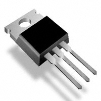
引脚分配:1=栅极(Gate),2=漏极(Drain),3=源极(Source)。
参数特性:
- 漏源击穿电压(V(BR)DSS):400V
- 漏源漏电流(IDSS):0.25mA (在VDs=400V, VGs=0V时)
- 栅源正向漏电流(IGSSF):100nA (在VGsF=20V, VDs=0V时)
- 栅源反向漏电流(IGSSR):-100nA (在VGSR=-20V, VDS=0V时)
- 栅阈值电压(VGs(th)):2.0V至4.0V
- 静态漏源导通电阻(Rds(on)):0.4Ω至0.55Ω (在Vas=10V, ID=5.0A时)
- 正向跨导(gFS):4.0S (在VDs=15V, ID=5.0A时)
- 输入电容(Ciss):1570pF (在VDs=25V, VGs=0V, f=1.0MHz时)
- 输出电容(Coss):230pF
- 反向传输电容(Crss):55pF
- 总栅电荷(Qg):46nC至63nC (在VDs=320V, ID=10A, VGs=10V时)
- 栅源电荷(Qgs):10nC
- 栅漏电荷(Qgd):23nC
- 内部漏感(Ld):4.5nH (从漏极引线0.25英寸处测量至芯片中心)
- 内部源感(Ls):7.5nH (从源极引线0.25英寸处测量至源极焊盘)
- 二极管正向电压(VsD):2.0V (在Is=10A, VGs=0V时)
- 反向恢复时间(trr):250ns (在IF=10A, di/dt=100A/us时)
功能详解:
IRF740适用于高电压、高速应用,如电源、PWM电机控制和其他感性负载。雪崩能量能力被指定以消除在感性负载被切换时的设计猜测,并提供额外的安全边际以防止意外的电压瞬变。
应用信息:
IRF740特别适用于需要高能雪崩模式和高效开关的应用场合,例如电源、PWM电机控制等。
封装信息:
IRF740采用的是TO-220AB封装。