SPECIFICATION FOR APPROVAL
DOCUMENT
: SRL40000NH
REVISION
: A0
PAGE
: 1 OF 7
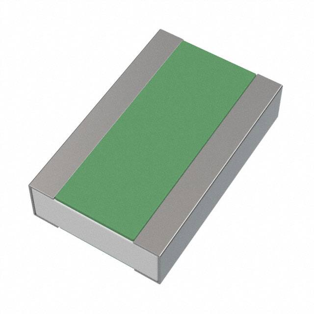
1/2W, 0805 Low Resistance Chip Resistor (Lead / Halogen free)
1. Scope
This specification applies to 1.2mm x 2.0mm size 1/2W, fixed metal film chip resistors rectangular type
for use in electronic equipment.
2. Type Designation
RLW2012 — 4 — □□□□
(1)
(2)
(3)
Where
(1) Series No.
(2) Power rating
4 = 1/2W
(3) Resistance value:
For example—
R005 = 0.005 Ω
(4) Resistance tolerance:
F= ± 1%
G= ± 2%
J= ± 5%
□
(4)
3. Construction and Physical Dimensions
Code Letter
Dimensions (mm)
L
1.3 ± 0.20
W
2.0 ± 0.20
t
0.50 ± 0.20
a
0.35 ± 0.15
b
0.35 ± 0.15
NOTE:
① Resistive element
( under protection film )
② Electrode
③ Protection film
④ Substrate
Figure 1.
Structure (No mark)
�SPECIFICATION FOR APPROVAL
DOCUMENT
: SRL40000NH
REVISION
: A0
PAGE
: 2 OF 7
4. Ratings
4-1 Specification
Power Rating*
1/2 W
Resistance Range
0.005Ω~0.030Ω
Resistance Tolerance
±1% , ±2% , ±5%
0~200ppm/℃
Temperature Coefficient of Resistance
Note*:
Power Rating is based on continuous full load operation at rated ambient temperature of 70℃.
For resistors operated at ambient temperature in excess of 70℃, the maximum load shall be
derated in accordance with the following curve.
%
100
Percentage of the
rated dissipation
50
0
-55
70
125
Ambient temperature
Figure 2
Derating Curve
4-2 Rated Voltage
The rated voltage shall be determined by the following expression.
V = P× R
Where V:Rated voltage (V)
R:Nominal resistance value (Ω)
P:Rated dissipation (W)
4-3 Operating and Storage Temperature Range
-55 to +125℃
℃
�SPECIFICATION FOR APPROVAL
DOCUMENT
: SRL40000NH
REVISION
: A0
PAGE
: 3 OF 7
5. Characteristics
Test Item
Condition of Test
Requirements
Short Time Overload
5 * Rated power for 5 seconds
Refer to JIS C 5201-1 4.13
∆R : ± (0.5%+0.0005Ω)
Without significant damage by
flashover ( spark, arching ), burning
or breakdown etc.
Insulation Resistance
The resistor shall be cramped in the
metal block and tested , as shown below.
Test voltage : 100 ± 15VDC for 1 minute
Refer to JIS C 5201-1 4.6 Mounting
condition G.
Between Electrode and Protection
Film 100MΩ or over
Between Electrode and Substrate
1,000MΩ or over
Voltage Proof
The voltage : 100VAC (rms.) for 1 minute ∆R : ± (1.0%+0.0005Ω)
Refer to JIS C 5201-1 4.7
Without damage by flashover, fire
or breakdown, as shown below.
Thermal Shock
-55 ~125℃ 5 cycles, 15 min at each
extreme condition
Refer to JIS C 5201-1 4.19
∆R : ± (1.0%+0.0005Ω)
Without distinct damage in
appearance
Low Temperature Storage
Kept at -55℃, 1,000 hours
Refer to JIS C 5201-1 4.23.4
∆R : ± (1.0%+0.0005Ω)
Without distinct damage in
appearance
High Temperature Exposure
Kept at 125℃ for 1,000 hours
Refer to JIS C 5201-1 4.23.2
∆R : ± (1.0%+0.0005Ω)
Without distinct damage in
appearance
Solderability
Temperature of Solder : 245 ± 5℃
Immersion Duration : 2 ± 0.5 second
Refer to JIS C 5201-1 4.17
Uniform coating of solder cover
minimum of 95% surface being
immersed
Resistance to Soldering Heat
Dipped into solder at 270 ± 5℃
for 10 ± 1 seconds
Refer to JIS C 5201-1 4.18
∆R : ± (0.5%+0.0005Ω)
Without distinct deformation in
appearance
�SPECIFICATION FOR APPROVAL
Test Item
Condition of Test
DOCUMENT
: SRL40000NH
REVISION
: A0
PAGE
: 4 OF 7
Requirements
Load Life
Rated voltage for 1.5 hours followed by a
pause 0.5 hour at 70 ± 2℃.
Cycle repeated 1000 hours
Refer to JIS C 5201-1 4.25
∆R : ± (1.0%+0.0005Ω)
Without distinct damage in
appearance
Damp Heat with Load
40 ± 2℃ with relative humidity 90% to
95%. D.C. rated voltage for 1.5 hours
ON and 30 minutes OFF. Cycle
repeated 1,000 hours
Refer to JIS C 5201-1 4.24
∆R : ± (1.0%+0.0005Ω)
Without distinct damage in
appearance
Mechanical Shock
100 G’s for 6milliseconds. 5 pulses
Refer to JIS C 5201-1 4.21
∆R : ± (0.5%+0.0005Ω)
Without mechanical damage such
as break
Bending Test
Glass-Epoxy board thickness : 1.6mm
Bending width : 2mm
Between the fulcrums : 90mm
Refer to JIS C 5201-1 4.33
∆R : ±(1.0%+0.0005Ω)
Without mechanical damage such
as break
�SPECIFICATION FOR APPROVAL
DOCUMENT
: SRL40000NH
REVISION
: A0
PAGE
: 5 OF 7
6. Recommended Solder Pad Dimensions
Note :
We recommend there is no circuit design between pads to avoid circuit short
�SPECIFICATION FOR APPROVAL
DOCUMENT
: SRL40000NH
REVISION
: A0
PAGE
: 6 OF 7
7. Packaging
7-1 Dimensions
7-1-1 Tape packaging dimensions
1.5
+-
0.6 ± 0.10
0.1
0.0
Sprocket hole
4.0 ± 0.1
1.75 ±0.1
A
CHIP
3.5 ± 0.05
8.0 ± 0.3
B
0.65 ± 0.10
4.0 ± 0.1
Carrier cavity
2.0 ± 0.05
Pull Direction
※ Pre-emptied holes : 150 holes (or 30cm) or more.
Code letter
A
B
Unit : mm
1.45 ± 0.10 2.25 ± 0.10
Dimension
7-1-2 Reel Dimensions (Plastic reel : Correspond with EIAJ RRV08B)
13 ± 1.4
50
105
2
13 ± 0.2
+1
60-0
28 ± 0.8
R1
+0
180-3
Label
105 x 50
9 ± 0.3
Unit : mm
�SPECIFICATION FOR APPROVAL
7-2 Peel force of top cover tape
The peel speed shall be about 300 mm / min.
The peel force of top cover tape shall be between 0.1 to 0.7 N.
Top Cover Tape
165 ~ 180°
0.1~0.7 N
7-3 Numbers of taping
5,000 pieces / reel
7-4 Making
The following items shall be marked on the reel.
(1) Type designation
(2) Quantity
(3) Manufacturing date code
(4) Manufacturer’s name
(5) The country of origin
DOCUMENT
: SRL40000NH
REVISION
: A0
PAGE
: 7 OF 7
�
RLW-2012-4-R017-FNH 价格&库存
很抱歉,暂时无法提供与“RLW-2012-4-R017-FNH”相匹配的价格&库存,您可以联系我们找货
免费人工找货